Note: Descriptions are shown in the official language in which they were submitted.
CA 02261139 1999-O1-15
WO 98/03842 PCT/FI97/00451
1
SPECTROMETER
The present invention concerns a spectrometer
as defined in the preamble to Claim 1. The invention
particularly concerns an LED (light emitting diode)
spectrometer operating without moving parts, applying
the sweep principle, and intended to be used as a
structural component in measuring apparatus.
It is possible, by means of designs based on
a line of LEDs and on stationary grating optics, to
implement a sweep spectrometer operating without mov
ing_.parts and appropriate to be used for structural
component in a wide variety of spectroscopic concen-
tration analysers and colorimetric instruments. In
such measuring apparatus, information is gained con-
cerning chemical composition. colour or any other
physical characteristic of a sample by means of meas-
uring the transmission or reflection spectrum from the
sample in a given, desired wavelength range. Present
technology enables LED radiation sources to be pro-
duced at least for the wavelength range from 430 to
4800 nm; it is therefore possible, in principle, to
utilize a spectrometer based on an LED radiation
source, in widely different measurement applications
in the visible light and infrared ranges. The best
chances for application of the LED spectrometer are
perhaps to be found in the wavelength range under 1100
nm; representing a well-tested, mature branch of tech-
nology, LED radiation sources in this range are avail-
able from a number of commercial manufacturers, as
high power, favourably priced components. One of the
practical applications that can be contemplated thus
consists pf measurement of fat, albumin and water con-
tent of foodstuff raw materials, which are carried
. out, at present, with concentration analysers based on
measuring the 800 to 1050 nm transmission spectrum.
CA 02261139 1999-O1-15
WO 98/03842 PCT/FI97/00451
2
The LED spectrometer has been further devel-
oped in recent years, in a variety of projects. The
construction and operating principle of an adjustable
LED radiation source that has been worked out is known
through the International Patent No. WO 88/10462. The
design described in this reference presents the sali-
ent feature that the intensity of the output beam from
an LED radiation source module is controlled, or main-
tained constant, by measuring this intensity and, on
the basis of such measurement, adjusting the current
passing through the respective LED. The apparatus dis-
closed by the reference comprises, as an essential
component thereof, a beam divider, a monitoring detec-
tor, and appropriate signal processing, so that it
might be possible during operation to measure the in-
tensity of the output beam.
Furthermore, there is known, through Interna-
tional Patent No. WO 94/15183, a spectrometer radia-
tion source and its tuning arrangement. The radiation
source of said reference, comprising a light element
base and a plurality of light elements, these light
elements being disposed on said light element base in
linear array with a given spacing, and optics means
disposed in conjunction with the radiation source, for
collecting the radiation produced by the light ele-
ments, for dispersing it to a predetermined wavelength
spectrum and for aiming it at the object of measure-
ment, will produce between 2 and 16 measuring wave-
length bands having comparatively narrow half-value
widths. Moreover, by the aid of the tuning arrangement
described in the reference, tuning of the radiation
source is performed, this operation comprising such
adjustment of the locations in relation to each other
of the optics and light elements that wavelength bands
can be formed such as are desired.
It has been successfully demonstrated by
means of the above-described, implementation designs
CA 02261139 1999-O1-15
WO 98/03842 PCT/FI97/00451
3
of the first generation spectrometer, based on LED
technique, that this technique is generally opera-
tional; and potential applications of the technique
- have been successfully studied e.g. in concentration
measuring apparatus in foodstuff industry. However,
any introduction of the LED spectrometer in its use as
a core component of industrially manufactured concen
tration analysers, and colorimeters, implies substan
tially enhanced performance and/or less expensive
manufacturing, compared with the spectrometer technol-
ogy presently employed in measuringapparatus of this
kind. Existing types of apparatus are most commonly
based on using an incandescent lamp for radiation
source and a swivelling grating serving the task of
spectral dispersion (sweeping grating spectrometer>,
on a rotating filter disk carrying a plurality of in-
terference filters, or a stationarily mounted combina-
tion of grating and detector array. With implementa-
tion designs of the LED spectrometer known up to date
no substantially superior technical level of perform-
ance or significantly lower manufacturing costs were
achieved which would have resulted in any extensive
acceptance of LED techniques as a principle for imple-
menting concentration and colour analysers.
In the following is presented a synopsis,
based on studies made using experimental apparatus, of
the technical problems of first generation LED spec-
trometry and of its inherent limitations in applica-
tions relating to foodstuff raw materials. What is
held forth here is also extensively applicable in re-
Bard to other practical applications based on spectral
measurement or colorimetry.
Typically, an LED spectrometer module suited
for measurements on foodstuffs is desired to produce
at least 32, spectrally~narrow measuring bands in a
wavelength range covering, at least, the wavelengths
between 830 and 1050 nm, and one desires to use the
CA 02261139 1999-O1-15
WO 98/03842 PCT/FI97/00451
4
module in measurements of the transmission spectra of
foodstuffs. Typically, one desires to measure the ab-
sorbance spectrum on the level of 2 to 4 O.D., equiva-
lent in terms of sample transmittance to a range of T
- 0.01 to 0.0001 (Absorbance = 1og10(1/T)). It is fur-
ther desired that the amplitude/noise ratio of the
spectrum which is measured be 103 to 10q. For these
reasons, the optical power of the spectrometer's out-
put beam has to be high - at least 7 to 8 decades over
the noise level of the receiver - in order that the
desired signal/noise ratio might be achieved when
measuring powerfully attenuating samples. The optical
efficiency and output beam power of LED spectrometry
of prior art only meet the requirements in the best
spectrum bands, while the greatest problems are en-
countered on the extreme fringes of the wavelength
scale, 830 to 850 nm and 1000 to 1050 nm.
Secondly, utilization of a multiple channel
spectrometer in a concentration analyser implies that
a calibration is made, which is usually based on meth
ods of multiple component analysis (PLS, for in-
stance). The search for the calibration parameters
necessitates measurements on extensive series of sam-
ples, and performing any concentration measurements by
means of a reference procedure. Working out a good
calibration often constitutes an exacting task requir-
ing much time and involving expenses. It is therefore
desirable that calibrations worked out for commercial
concentration analysers can be transferred to other
equivalent analysers. The previous LED spectrometer
fails to meet the requirements imposed by such cali-
bration transfer because the wavelengths of the spec-
tral bands produced by individual LED radiation
sources are only identical within about ~ 2 to 5 nm.
As a consequence, every concentration measuring device
has to be separately calibrated. It has been learned
from experience gained in measurements on foodstuffs
CA 02261139 1999-O1-15
WO 98/03842 PCTIFI97/00451
that calibrations are easier to transfer if the cen-
tral wavelengths of the bands are identical within
error limits of ~ 0.3 to ~ 0.5 nm when operating in
the 830 to 1050 nm wavelength range.
5 Thirdly, the wavelength of the radiation pro-
duced by the LED source and its intensity are strongly
dependent on temperature: typically, the intensity
from an LED component decreases, and the wavelength
increases, with increasing operating temperature. It
is possible to stabilize the untensity of an LED spec-
trometer's measuring beam by measuring the intensity
of the output beam and controlling the current of the
respective LED. As for wavelength, the temperature
dependence of an LED spectrometer is less than the
wavelength dependence of the LED alone: the grating
optics delimits the measuring beam to a narrow spec-
tral band and attenuates the changes in wavelength due
to temperature. In spite of what has just been said,
the temperature dependence of the central wavelengths
of the LED spectrometer module described in the fore-
going is about 0.3 nm per 1.0°C, at its maximum. Tem-
perature dependence of the output beam's wavelength in
this magnitude may well give rise to errors of meas-
urement in a concentration analyser based on spectros-
copy, in the case of varying ambient conditions.
Fourthly, the radiation should be completely
damped out in the inhibition band outside the measur-
ing band, in an ideal spectrometer. In spectrometers
based on use of an interference filter, as a rule,
transmission is less than 0.1o in the inhibition band.
In LED spectrometers, many of the measuring bands are
. produced from the marginal areas of the respective
LED's emission spectrum. If the intensity from the LED
at the wavelength of a given, desired measuring band
is no more than 10°s of the peak wavelength intensity,
achieving three decades attenuation in the inhibition
band in the measuring beam implies, in practice, four
CA 02261139 1999-O1-15
WO 98/03842 PCT/FI97/00451
6
decades attenuation at the LED's peak wavelength.
Typical LED chips radiate into semispace, and part of
the cone of radiation strikes the enclosure of the
module structure. Therefore, part of the radiation may
be scattered or reflected back to the output slit and
thus be propagated along with the measuring beam. Ow
ing to these problems, sufficient inhibition band at
tenuation is not achieved in the case of the weakest
measuring bands, in the LED radiation source module of
prior art.
The objective of the present invention is to
abolish the problems brought Forth in the foregoing.
Specifically, the object of the present invention is
to disclose a spectrometer of novel type in which the
technical problems described above can be avoided.
It is a further objective of the present in-
vention, to disclose a spectrometer by the aid of
which any desired number of radiation spectra can be
produced, at different wavelengths, and in which the
calibration made with one spectrometer can also be
used in measurements carried out with other equivalent
spectrometers.
It is furthermore an objective of the present
invention, to disclose a spectrometer which is amena
ble to being advantageously industrially manufactured
and which can be produced employing generally avail-
able industrial methods and subcontracting facilities.
Regarding the features characterizing the
invention in hand, reference is made to the claims.
The spectrometer of the invention comprises a
radiation source, comprising a light element base and
a plurality of light elements, these light elements
being arranged on the light element base in linear
array, with predetermined spacing. Furthermore, the
spectrometer of the invention comprises optical means
disposed in connection with the radiation source, to
collect the radiation produced by the light elements,
CA 02261139 1999-O1-15
WO 98/03842 PCT/FI97/00451
7
to disperse it to a predetermined wavelength spectrum,
and to guide it to the object under measurement. The
spacing of light elements located side by side in
principle, and the linear wavelength dispersion
(Ox/~~,) are so dimensioned that, for each light ele-
ment, the, spectrum band of desired wavelength will
emerge through the spectrometer's output slit. As
taught by the invention, the radiation source com-
prises a reflector base, disposed in conjunction with
the light element base, on which the the light ele-
ments have been arranged and which comprises, assigned
to each light element and disposed in conjunction with
each light element, a concentrator for directing the
radiation emitted by each light element into a prede-
termined solid angle. Advantageously, each concentra-
tor has been formed by embossing in the reflector base
a depression of predetermined shape, the configuration
of its bottom substantially matching the shape of the
light element and the size of said bottom equivalent
to the size of the entire light element augmented by
allowable positioning tolerance, this bottom configu-
ration being usefully applied in accurately position-
ing the LED chips. The concentrator may be a concen-
trator of non-imaging type such as is commonly de-
scribed in the relevant literature.
In an advantageous embodiment of the present
invention, the light elements are arranged in two par-
allel rows in such manner that adjacent light elements
are intercalated. By this construction, smaller size
is achieved in designing the light sorce and optics.
Advantageously, the reflector base as well as the re-
flector surface of the concentrator is coated with a
reflecting substance.
In an advantageous embodiment of the present
invention, the reflector base is made of electrically
and thermally conductive material, such as copper, for
instance. Advantageously, the radiation source incor
CA 02261139 1999-O1-15
WO 98/03842 PCT/FI97/00451
8
porates a measuring element connected in thermally
conductive fashion with the reflector base, for meas-
urement of its temperature. The radiation source
moreover comprises a Peltier element connected in
thermally conductive fashion with the reflector base,
close to the light elements, for cooling and/or heat-
ing the radiation source. This allows efficient com-
pensation for the warming-up of the LEDs, as well as
rendering constant the wavelength of the radiation
which they emit. In addition, the measuring element of
the present invention, the Peltier element and the
thermal structure of the LED, in combination, enable
temperature stabilization to be provided, by the aid
of which the temperatures of the LED elements are
maintained constant during operation. The intensities
and wavelengths of the LED spectrometer's bands will
then be constant in spite of variations in ambient
conditions. Thus, the stability in operating condi-
tions of the concentration measuring apparatus or col-
orimeter can be improved without recourse to measuring
the output beam intensity and without control, on the
basis of this measurement, of the current passing
through the respective LED, as disclosed in the above-
cited reference WO 88/10462.
Furthermore, electrical leads are provided on
the light element base for elctric supply of the light
elements, and the light elements are attached to the
reflector base with an electrically conductive sub-
stance, electrical contact with each light element
being provided from the reflector base.
In an advantageous embodiment of the present
invention, the radiation source comprises a window
element, disposed substantially above the light ele-
ments and concentrators, to protect them against ambi-
ent influence. Moreover, the intervening space between
this window element and the light elements is filled
CA 02261139 1999-O1-15
WO 98/03842 PCTIFI97/00451
9
with translucent substance, such as extra pure epoxy
or silicone.
In an advantageous embodiment, the radiation
source comprises an output slit, disposed in the vi
cinity of the radiation source, and an optical fibre,
connected to the output slit, for conducting the ra-
diation emerging from the output slit, to the object
under measurement.
In an advantageous embodiment of the present
invention, the optical means comprise a first prism,
disposed substantially adjacent to the radiation
source to receive radiation emitted by the radiation
source; a plane mirror provided with a piercing aper
ture for letting the radiation emitted by the radia
tion source to pass through the plane mirror; a second
prism, communicating through the plane mirror with the
first prism; a reflection grating for dispersing the
radiation emitted by the radiation source to a wave-
length spectrum; and a concave mirror, at a distance
from the radiation source and disposed in conjunction
with the second prism to reflect the radiation onto
the reflection grating and through the pass-through
aperture to the output aperture. Advantageously, the
wavelength spectrum generated with each light element
is arranged to pass through the pass-through aperture,
to be reflected by the concave mirror onto the reflec
tion grating and from the reflection grating over the
plane mirror and concave mirror, once again through
the pass-through aperture and further to the output
slit.
Further, in an embodiment of the invention,
the locations with reference to each other both of the
light elements, plane mirror, concave mirror, reflec-
tion grating and the output slit are so arranged that
at the output slit a different wavelength spectrum is
produced in correspondence with each light element.
CA 02261139 1999-O1-15
WO 98/03842 PCT/FI97/00451
The advantage of the present invention over
previously known technology is optical power output in
the beam proceeding through the output slit, demon-
strated by measurements to be about fivefold compared
5 with that of the previous LED spectrometer module. The
enhancement of power output is a result of increased
numerical aperture of the LED radiation source and of
the optical means, and to increased transmission. This
increased optical power output renders possible meas-
10 urements with good signal/noise ratio on strongly at-
tenuating foodstuff samples. Moreover, at the extremes
of the wavelength scale the increment is even greater
than this, owing to new LEDs which have been intro-
duced in the radiation source.
Further, thanks to the invention, it now be-
comes possible in the location of the elements of the
LED radiation source to achieve requisite accuracy of
positioning, whereby better matching is attainable
between the wavelength scales of individual LED spec-
trometers which are being manufactured. We have been
able, employing the techniques of the invention, to
turn out four LED spectrometer modules having identi-
cal central wavelengths within ~ 0.4 nm. Good repro-
ducibility of wavelength scales affords better chances
than many competitive techniques can claim, for cali-
bration transfer from instrument to instrument.
In addition, thanks to the present invention,
diffuse light occurring in the spectral inhibition
band has now been brought down to the same level as in
spectrometers based on interference filters. Measure-
ments performed in a trial have shown that the diffuse
light is below 0.1% on most channels and even on the
faintest channels, less than 0.3% of the band's peak
intensity, as measured at ~ 36 nm distance from the
central wavelength of the band.
It is a further advantage of the invention
over the state of art, that the construction of the
CA 02261139 1999-O1-15
WO 98/03842 PCT/FI97/00451
11
LED spectrometer of the invention is well suited for
industrial manufacturing, involving reasonable manu-
facturing costs. The components of the LED radiation
source and of the optics can all be produced by means
of commonly used procedures, using available subcon-
tracting facilities. The construction incorporates no
"fenestrated" grating as previous LED radiation
sources do; such gratings have the drawbacks of lim-
ited availability and high price. Instead, the present
design uses a reflection grating of standard type.
In the following, the invention is described
with the aid of attached embodiment examples, refer-
ring to the attached drawing, wherein:
Fig. 1 presents, schematically, an LED spec-
trometer according to the invention;
Fig. 2a displays a group of LED radiators
produced on a reflector base, according to the inven-
tion;
Fig. 2b displays the design of the LED radia
tion source and the principle of dimensioning the con
centrators;
Fig. 2c displays a reflecting depression ac
cording to the invention and illustrates the utiliza
tion of its bottom in accurate positioning of the LED
chip;
Fig. 3 presents an implementation of the op-
tical means, according to the invention; and
Fig. 4 presents the coating arrangement of a
plane mirror.
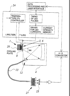
Fig. 1 presents the principle diagram of an
LED spectrometer conforming to the invention. The
spectrometer includes an LED radiation source 1 with
light elements 3. In conjunction with each light ele-
ment, an optical concentrator 6 has been provided,
which concentrates the radiation from the light ele-
ment in a solid angle arranged to equal the numerical
aperture of the spectrometer. To the radiation source
CA 02261139 1999-O1-15
WO 98/03842 PCT/FI97/00451
12
1, in conjunction with the reflector base, has been
attached, in thermally conductive fashion, a Pettier
element 8, by the aid of which the heat generated by
the light elements 31 ... 3° is transported over a
cooling plate 20 to ambient air, in order to stabilize
the radiation wavelength.
Furthermore, a control electronics assembly
24 has been connected to the radiation source, con-
taining a temperature controller and timing and drive
circuits associated with the task of pulsing the light
elements. The temperature controller is advantageously
implemented as a PI controller, and it is connected to
the radiation source, to monitor representatively the
temperature of the light elements 31 ... 3n. The tem-
perature controller is further connected with the
Pettier element 8 so that it becomes possible, as re-
quired, to cool or to heat the light elements 31 ... 3°
by mediation of the reflector base 5. The parameters
of the temperature controller are preset so that the
temperature controller will keep the temperature of
the light elements substantially constant during the
LED spectrometer's operation regardless of the waste
heat produced by the apparatus and of any variations
of ambient temperature within the normal operating
temperature range, e.g. in the ambient temperature
range from 0 to +50°C.
The timer circuits incorporated in the con-
trol electronics generate control pulses for each one
of the light elements 31 ... 3°, which switch on one
light element at a time, in succession. The duration T
of these control pulses is advantageously 100 to
500 ~.s, and each pulse switches on the respective
light element for a period substantially equalling the
pulse length. Each drive pulse is advantageously fol-
lowed by a pulse interval of equal length, during
which none of the light elements is activated. Thus,
the sweep time needed to activate all light elements
CA 02261139 1999-O1-15
WO 98/03842 PCT/FI97/00451
13
31 ... 3° totals 2*T*n, whereafter the operation is
continuously repeated. In the case of a typical LEC
spectrometer containing 32 light elements, the sweep
frequency will thus lie between 20 and 200 Hz.
S A drive circuit associated with each light
element switches on the stabilized drive current to
the light element for the duration of the control
pulse. For each light element a drive current has been
selected, its intensity advantageously between 10 and
1000 mA. The drive current intensities have been
stored in a current memory carrying one or several
sets of intensities for all light elements. This cur-
rent memory is implemented by providing exchangeable
current setting resistors for each light element, or
by providing electronically settable current setting
resistances for each light element, or by storing the
current intensity values in an electronic memory cir-
cuit included in the drive circuits. A plurality of
current intensity sets can be utilized in order to
adapt the operation of the LED spectrometer so that
maximum signal/noise ratio will be achieved in meas-
urements on samples characterized by various optical
attenuation.
The LED spectrometer further contains optical
means 4 fixedly mounted in conjunction with the ra
diation source, which serve to collect the radiation
produced by the radiation source, to disperse it to a
predetermined wavelength spectrum, and to concentrate
the spectrum on the output slit 12. Fig. 1 schemati
cally illustrates the implementation of these optical
means, employing a concave reflection grating. It is
equally possible to provide for equivalent operation
in the manner envisioned by the invention, also using
a reflection-type or transmission-type plane grating,
or a prism, to disperse the radiation to a predeter-
mined wavelength spectrum. Further reference is here
made to Fig. 3, which farther below presents an advan-
CA 02261139 1999-O1-15
WO 98/03842 PCT/FI97/00451
14
tageous mode, based on use of a reflection-type planar
grating, for arranging the optical means 4.
Behind the output slit 12, fibre optics 13
has been provided, by which the narrow spectral band
that has passed through the output slit can proceed
and impinge on the sample under measurement, 27. The
amplitude of the radiation that has passed through the
sample or has been reflected or scattered by it, car-
ries information about the sample's properties, in the
manner knwon in the art of spectroscopy or colorimet-
ric technology. At the detector 23, is obtained a ra-
diation pulse relating to each light element in turn
and to the spectral band therewith associated, this
pulse being converted to electrical form and amplified
to appropriate level. In an LED spectrometer disposed
to operate in the wavelength range of 800 to 1050 nm,
an Si photodiode advantageously serves as detector,
while with greater wavelengths Ge or InGaAsP photodi-
odes, for instance. may be used. The amplified light
pulses are converted to digital form by means of an
A/D converter, and the results are carried to a com-
puter responsible for data processing to serve the
concentration analyser or colorimeter, this computer
performing requisite mathematical procedures and
transferring the results from the measuring operations
to be accessible by the operator.
In Fig. 2a, a radiation source 1 conforming
to the invention is presented in greater detail, this
radiation source comprising 32 light elements 31, ...,
332, LED chips; a plurality of miniature-sized non-
imaging concentrators 61, . . . , 632 integrated with the
structure, in conjunction with each LED chip; and a
thermal construction enabling good temperature stabi-
lizing. In this connection, thermal construction is
understood to mean that the LED chips are joined with
the cold face of the Peltier element 8 and with the
temperature measuring element 7, through a thermally
CA 02261139 1999-O1-15
WO 98/03842 PCT/FI97/00451
well conductive reflector base 5, the LED chips are
bonded to the reflector base 5 by low heat resistance,
electrically conductive epoxy with silver filling, or
by special solder, and on the other hand the LED chips
5 are reasonably well insulated agaisnt ambient tempera-
ture variations by a poured epoxy or silicone mass 11
possessing high thermal resistance and by a cemented
glass construction 4 constituting the optical means.
The procedure by which the reflector base 5
10 of the radiation source 1 is produced guarantees re
producible dimensions of the group of non-imaging con
centrators 61, ..., 632 in series production. Further
more, the bottoms of the concentrators 61, . . . , 632 are
dimensioned to match the size of the LED chips 31,
15 ..., 332, augmented by allowable positioning toler-
ances, thereby serving as alignment markers when the
LED chips are being mounted, and enabling accurate
positioning of the chips. Experience has demonstrated
that it is possible by this procedure to keep the
positional errors of the elements in the radiation
source array below ~ 16 ~,m. This, in its turn, enables
the errors in wavelength of the bands produced by the
spectrometer incorporating the radiation source I to
be limited to be within ~ 0.3 to 0.5 nm on the wave-
length scale when using the optical arrangement of the
invention.
The reflector base 5 of the advantageous ra-
diation source of Fig. 2a is made of material having
good thermal conductivity, whereby the differential
temperatures between the LED chips 31, ..., 332 will be
minimal and the implementation of the temperature
pick-up 7 shown here will give a representative meas-
urement of the true temperature of the LED chips dur-
ing operation. Such representative temperature meas-
urement enables accurate temperature stabilizing to be
accomplished for the LED chips 31, . . . , 33z. Copper is
well suited for material to make the reflector base 5,
CA 02261139 1999-O1-15
WO 98/03842 PCT/FI97/00451
16
as regards thermal conductivity. Being a malleable
substance, it is also amenable to be embossed, using a
die pressing tool, to endow the array of non-imaging
concentrators 61, ..., 632 with desired shape. Copper
can be coated with a suitable reflector coating, e.g.
galvanic gold plating.
Still referring to Fig. 2a, the radiation
source 1 is composed of an array, produced in a copper
block with the aid of a die pressing tool, of 32 non-
imaging concentrators 61, . . . , 632 Of modified configu-
ration; of LED chips 31, ..., 332 mounted on the bottom
of said concentrators; and of a temperature pick-up 7
monitoring the temperature of the copper block, which
may be a miniature thermistor.
The practical implementation design of
Fig. 2a could, advantageously, contain 32 chips as
follows:
2 off, GaAlAs LEDs, with central wavelength
840 nm:
LEDs 31 and 32;
- 13 off, GaAlAs LEDs, with central wave-
length 880 nm:
LEDs 33 through 31s;
- 8 off, GaAs LEDs, with central wavelength
940 nm:
LEDs 316 through 3z3;
- 9 off, InGaAsP LEDs, central wavelength
1020 nm:
LEDs 324 through 33z .
The LED chips are about 0.30 by 0.30 by 0.20
mm in size. The section of thenon-imaging concentrator
6 of those reflector bases which have been made is
rectangular, cross secton on the bottom about 0.32 by
0.34 mm, at the front face about 0.64 by 0.70 mm, and
depth of the reflector about 0.50 mm. It was desired
to pack the 32 concentrated radiators comprised in the
radiation source in a tight array so as to achieve
CA 02261139 1999-O1-15
WO 98/03842 PCT/FI97/00451
17
small overall dimensions of the spectrometer. The
length of the array was chosen to be 12.0 mm, making
the spacing of consecutive LED radiators 0.387 mm. So
tight packing is not possible in one row using LED
chips of standard type and the dimensioning stated
above; therefore, the LED radiators are placed in two
side-by-side, suitably intercalated rows in an advan-
tageous embodiment. In conformity herewith, the size
of the output slit has been set to be long enough,
advantageously 0.7 mm by 2.5 mm, whereby the radiation
spectra produced in the parallel rows will be imaged
on one and the same output slit, by ef fect of the ge-
ometry of the optical means. The dimensioning of the
non-imaging concentrator 6 and its use for optics
matching the concentrators, detectors and light
sources is known in the literature. Fig. 2b displays a
non-imaging concentrator dimensioned according to
methods described in the literature by which it is
possible to collect the radiation emitted into semis-
pace by any planar light source, in its entirety, and
to direct it into a solid angle of desired magnitude.
In the design solution of the invention, the
configuration of the non-imaging concentrator 6 is
calculated, following the idea shown in Fig. 2b. The
concentrator 6 is dimensioned to receive a cone of
radiation emitted into semispace by the LED chip 3,
and to direct it into asmaller solid angle consistent
with the spectrometer's NA (NA = numerical aperture).
It is thus possible in principle, when using the ra-
diation source 1 of the invention, to collect 100 0 of
the radiation emitted by the LED chip, into the input
aperture of the spectrometer optics 4. This design
results in improved optical efficiency and, conse-
quently, in improved attainable signal/nois ratio of
the spectrometer. It moreover improves the attenuation
in the non-pss band because collection of the beam
will minimize the radiation falling outside the input
CA 02261139 1999-O1-15
WO 98/03842 PCT/FI97/00451
18
aperture, which radiation often tends to become cou-
pled with the output beam, to constitute a signal pre-
sent in the inhibition band. In practice, the col-
lected cone is broadened by any non-ideal features of
the non-imaging concentrator construction, such as
departure from ideal reflector shape, surface quality
and implementation of the concentrator with curtailed
length, and the proportion of the cone directed into
the NA of the spectrometer, relative to the radiation
emitted by the LED chip, is thus somewhat reduced by
their effect.
Referring further to Fig. 2b, and to Fig. 2c,
the base plate 2 of the radiation source is made of
A1203 ceramics, and the conductor patterns required for
electric connection of the LED array have been printed
on it by means of thick film technique. All LED chips
31, ..., 332 get their common bottom contact through
the reflector base 5. The chips 31, . . . , 332 are fixed
- on the reflector base 5 with conductive epoxy, or by
soldering. From the contact base on the top face of
each chip 31, ..., 332, a wire contact 9 has been
bonded with 25 ~,m gold wire, or equivalent, to the
thick film wiring, whereby the LED radiators
31, ..., 332 can be individually activated with the
drive current. The LED radiators are protected by a
window element 10, and the intervening space between
the windon and the LED elements is filled with trans-
parent, extra pure epoxy or silicone 11 for protection
of the semiconductor chips against ambient influence,
and for matching the refractive index of the medium to
be closer to that of the GaAs and InGaAsP materials.
Such refractive index matching improves the coupling
efficiency at the interface of the LED chips 31, . . . ,
332 and the transmitting medium, and minimises the
reflections occurring from the window 10 of the con-
struction.
CA 02261139 1999-O1-15
WO 98/03842 PCT/FI97/00451
19
In Fig. 2c is presented a concentrator ar-
rangement in which the bottom of the concentrator is
utilised in positioning the LED chip 3. The side
length B of the LED chip is 300 ~,m in this exemplary
case. The length of the bottom A, in the direction of
the row, is advantageously selected to be 320 Vim,
whereby the bottom allaws a positioning error of the
chip, in the direction of the row, of ~ 10 Vim. The
tolerance of positioning of the chip in the direction
across the row is not subject to the same requirement
as that longitudinally to the row, because errors in
positioning incurred in transverse direction cause no
errors in wavelength. With this understanding, the
bottom breadth in transverse direction has been se-
lected to be 340 ~tm, leaving a potential transverse
positioning error amounting to ~ 20 ~.m.
Fig. 3 presents the design of an LED spec-
trometer module according to the invention, and of its
optics 4, which has been implemented as an integral,
cemented glass construction. The optics 4 consists of
a first and a second prism 14,17 serving as a frame
structure and medium; a plane mirror 15 interposed
between them; a concave mirror 19; an absorber 22; and
a reflection grating 18 cemented under the structure.
The mirror coating 25 has been removed from a region
in the centre of the plane mirror 15, minimizing the
area of the aperture in the manner seen by reference
to Fig. 3, involving loss of no more than 250 of the
mirror area, whereby the cone of radiation from the
LED radiation source, indicated by a dotted line 26,
is admitted through said aperture to impinge on the
concave mirror 19, and similarly the cone coming from
the concave mirror can proceed to the output slit 12.
Behind the output slit 12, an optical fibre, or fibre
bundle, 13 has been affixed to carry the output beam
to the sample being measured.
CA 02261139 1999-O1-15
WO 98/03842 PCT/FI97100451
Furthermore, the spectrometer module depicted
in Fig. 3 comprises a radiation source 1, disposed
close to the output slit 12. To the radiation source 1
has been attached in thermally conductive fashion, a
5 Peltier element 8, by the aid of which the heat gener-
ated by the light elements 31, ..., 3° is transferred
through a cooling plate 20 to ambient air, in order to
stabilize the radiation wavelength.
It is thus understood that the LED spectrome
10 ter of the invention comprises, as an eminently sig
nificant component, sn optics module 4 designed to be
fixedly joined in conjunction with the LED radiation
source 1, this module making the assembly into an
electrically controlled sweeping spectrometer operat
15 ing without moving parts. The LED spectrometer optics
assembled in the form of a cemented glass construction
is known in prior art through the reference
WO 94/15183, cited above. The LED spectrometer optics
4 differs from prior art in its optical arrangement
20 and in its mode of operation. Thanks to the changes
that are apparent, the reproducibility of the LED
spectrometer's wavelength scales, its optical effi
ciency and its manufacturability as an industrial com
ponent are substantially superior to those of the ear
lier design.
Implementation of the optics by the design
based on mirror optics 4, as shown in Fig. 3, with
glass as optic medium, has enabled high numerical ap-
erture to be achieved. The high NA of the construction
(NA = 0.52, corresponding to f number 1.0) maximizes
the collection efficiency for the radiation from the
radiation source 1. The transmission of the optics, at
central wavelength of the pass band, is 20 to 400. The
angles in the prism, mirror and grating construction
have been so dimensioned that the grating 18 operates
in autocollineation, as viewed in the plane of the
spectrum, when the centremost element of the radiation
CA 02261139 1999-O1-15
WO 98/03842 PCT/FI97/00451
21
source 1 is activated. With an advantageous grating 18
having 1400 lines per mm, the angle of the plane mir-
ror 15 relative to the optic axis is then 32°, and the
plane wave produced by the centremost LED meets the
grating 18 under the angle of 26°. The output beam
obtained through the output slit 12 will then be the
centremost band of the wavelength scale for wavelength
940 nm. The plane waves produced by the extreme ele-
ments in the radiation source I will then meet the
grating under angles of 19° and 33°, respectively,
whereby the output beam will contain the bands for
wavelengths 830 nm and 1080 nm, respectively.
Tuning the LED spectrometer to make the cen
tral point of its wavelength scale coincide with the
desired value is accomplished in connection with as
senbly, the LED radiation source 1 being correctly
aligned in relation to the optics 4 in this work step.
This adjustment is made in functional succession,
wherein the output beam is measured with a spectrome-
ter and the LED radiation source 1 is locked in sta-
tionary position with UV-curing optical cement when
the wavelength scale has become properly aligned.
In the following , the functioning of an ad
vantageous spectrometer shall be described, referrig
to Figs 1 and 3. During operation, the temperature of
the LED radiation source 1 is stabilized with the aid
of an external PI controller receiving its measurement
data from a thermistor 7 incorporated in the LED ra-
diation source and controlling the Peltier element 8
comprised in the construction. The elements of the LED
radiation source 1 are driven by means of current
pulses supplied in suitable succession. The length of
these drive pulses is typically between 100 and
500 ~,s; the current pulses have an amplitude between
10 and 1000 mA and the sweep frequency covering the
entire array is typically 20 to 200 Hz.
CA 02261139 1999-O1-15
WO 98/03842 PCT/FI97/00451
22
The activated LED element emits radiation
into semispace, the greater part of the radiation
striking the walls of a non-imaging concentrator 6.
The cone of radiation is directed by the reflecting
wall, through prisms 14,17, towards the concave mirror
19 of the LED spectrometer's optics, this mirror col-
lineating the beam back towards a plane mirror 15 in
inclined position. The plane mirror reflects a propor-
tion about 750 of the beam, down towards the grating
18. The spectral components of the beam are redirected
in different directions towards the plane mirror 15,
which reflects them back towards the plane mirror 19.
The cones of radiation corresponding to different
wavelengths are focussed by the concave mirror 19 to a
spectrum formed upon the output slit 12. The output
slit passes a narrow wavelength band having, typi-
cally, a spectral half-value width about 50 of the
whole wavelength range covered by the spectrometer;
that is, in an embodiment of the invention in connec-
tion with measurements on foodstuffs, when the wave-
length range is 830 to 1050 nm, the half-value width
of a single band will be 11.5 to 13.5 nm, according to
measurements. This output beam proceeds by the fibre
optics 13, to the sample under measurement. The inten-
sity of the beam passing through the sample or re-
flected by it is detected by the aid of a Si detector
23, amplified, and converted to digital form by means
of an A/D converter. The result from this measurement
is proportional to the transmission or the reflectiv-
ity of the sample at the respective wavelength of the
measuring beam.
The light elements 31, . . . , 332 of the LED
radiation source 1 are all activated in similar way,
each one in turn. The optics 4 creates respective
spectra on the output slit 12, so that all 32 wave-
length bands, one after the other, are obtained as
output beam, covering the scale from 830 nm
CA 02261139 1999-O1-15
WO 98/03842 PCTlFI97/00451
23
to 1050 nm. Taking into account the geometry of the
sample arrangement, the transmission or reflection
spectrum of the sample on said wavelength scale can be
calculated from the measured signals.
Selection of the pulse currents supplied to
the LED radiation source can be utilized to make opti-
mal use of the A/D converter's dynamic range, to com-
pensate for differences in output power between LED
radiation sources, and to compensate for the spectral
attenuation caused by different kinds of samples. If
all these elements 31, . . . , 332 are driven at the same
current level, the power of the stronger spectral
bands of the measuring beam are typically up to ten-
fold, compared with the least powerful channels. The
LED elements of less powerful spectral bands can be
driven with current pulses of greater magnitude, thus
eliminating variations in power, or they may be lim-
ited to be less than 1 . 2. for instance. It is then
- possible to achieve substantially equal maximum S/N
ratio on all channels, and the dynamic range of the
converter will thus be optimally utilized without any
changes made in the gain of the amplifier stages dur
ing the fast pulsing sequence. The same technique can
be employed in order to optimize the spectrometer for
measurements of the transmission or reflection spec
trum of a given type of sample. Hereby the typical
spectral attenuation of a given sample, e.g. of a
foodstudd raw material; will be taken into account in
preselecting the currents for the LED elements
31, . . . , 332.
The invention is not exclusively delimited to
concern the embodiment examples presented in the fore
going: numerous modifications can be contemplated
within the scope of the inventive idea defined by the
claims.