Note: Descriptions are shown in the official language in which they were submitted.
CA 02261616 1999-O1-21
WO 98/04029 PCT/CA97/00459
1
LOW STRAY INTERCONNECTION INDUCTANCE POWER CONVERTING MODULE FOR CON-
VERTING A DC VOLTAGE 1NTU AN AC VOLTAGE, AND A METHOD THEREFOR
BACKGROUND:
In the past years, there has been a rapid growth in
the power electronic industry. This industry involves the
use of power electronic controlled switches. The function
of these switches is to sequentially close and open a
conductive link between two electrodes under the command
of an electric signal. The actual technology uses
semiconductor substrates to produce these switches,
therefore the switching time thereof is much faster than
switching time of the best mechanical relays. Because of
that, the power semiconductor switch is attractive for
electric power flow control. In these systems,
semiconductor switches are normally grouped with passive
elements in a defined configuration and connected between
an electrical power source and a load or another
electrical power source. Also, a series of voltage and
current sensors are provided to supply information to a
control unit where said information is analysed. Based
upon the analysed information, switching commands are
transmitted from the control unit to the switches so that
large amount of electrical energy can be exchanged between
sources in a controlled manner. These systems are better
known as power converters.
One common application of the power converter is for
driving an electrical motor. In this type of application,
a DC voltage source is generally used as the power supply
and a power converter is used to convert a DC voltage into
polyphase AC voltage to supply and control a polyphase AC
motor. These DC to AC power converters are also commonly
referred as inverters.
In order to supply high power to an electrical AC
CA 02261616 1999-O1-21
WO 98/04029 PCTlCA97100459
2
motor, the power converter requires switches that can
withstand high voltage and high current. In most known
configuration, the power converter operates the switches
in hard switching mode. In this mode, the switch goes from
a blocking state to a full conducting state in two steps.
In the first step, the current rises through the switch to
reach the load current as there is still a blocking
voltage across the switch. In the second step, the load
current circulates through the switch while the blocking
to voltage falls until a full conduction voltage drop is
reached across the switch. To go from full conducting
state to a blocking state, the same steps are achieved in
reverse.
During these two steps, the current-voltage product
is very high and generates switching power losses within
the electronic elements. These switching power losses are
added to the conduction losses of the switches and they
both generate heat. In order to avoid the destruction of
the electronic elements, their temperature must be kept
2o under a critical level. The cooling of the electronic
components is then achieved by means of a heat exchanger
joined side by side with the switching devices to release
the thermal energy. The size of this heat exchanger
depends directly on the amount of heat losses that is
generated which itself vary proportionately with the
switching frequency. On the one hand a converter operating
at a low switching frequency requires a smaller heat
exchanger. On the other hand, a higher switching frequency
is desired to reduce the size of the filter components and
the audible noise. Therefore, a compromise has to be made
in the choice of the operating switching frequency. To
reduce the size of the heat exchanger and the filter
components, to reduce the noise, and to increase the
efficiency of the power converter, the conduction and the
switching losses have to be reduced.
The today most commonly used switching elements in
CA 02261616 1999-O1-21
WO 98/04029 PCTICA97100459
3
power converters are gate capacitance transistors like
Mosfets, IGBTs or MCTs because they are easy to operate.
The conduction losses of these switching elements are in
relation with their physical properties, with their size
and with the fact that several of them can be mounted in
parallel. Accordingly little or nothing can be done for
reducing these conduction losses by acting on the way the
switching elements are controlled. For example, it is not
possible to act upon the conduction losses of Mosfets or
l0 IGBTs by working upon their control when their gate input
capacitance is fully charged. But it is possible to reduce
switching losses in cases where the switches are operated
in such way that one can still act upon the switching
losses by working on the way the switches are controlled.
Thus, the switching losses can be further reduced by
increasing the switching speed with the proper electrical
adjustment such as an appropriate choice of a gate
resistor for an IGBT or Mosfet. However, the power
electronic switching devices are then submitted to high
transient voltage spikes caused by abrupt changes in the
current that flows through the stray interconnection
inductance located within the power converter assembly.
These voltage spikes are added to the bus voltage. A
voltage combining the voltage spikes and the bus voltage
are then applied across the switch during the turn-off
phase. If the magnitude of the voltage spike becomes too
high, the switching electronic elements within the power
converter may be destroyed. In addition, the voltage spike
generates noise that affects other components in the
circuit through the stray capacitance elements and it also
adds to the EMI (Electromagnetic Interference) problem.
Also, just before the turn-off phase, it should be
noted that the energy stored in the magnetic field of the
' stray interconnection inductance will have to be released.
This energy is eliminated through heat losses within the
switches. In an article entitled "Losses due to Stray
CA 02261616 1999-O1-21
WO 98/04029 PCT/CA97/00459
Inductance in Switch Mode converters", by M. Fasching and
published in EPE Journal, Volume 6, No. 2, pages 33-36 of
September 1996, it is explained that additional power
losses in a converter can be linked to the stray
interconnection inductance when the switched-on current is
different from the switched-off current in the same
period, these losses contributing significantly to the
total losses of the power converter.
In order to reduce the voltage spike and to reduce
the switching losses of the converter, different
techniques may be applied.
First, a clamping device may be connected across the
switches to suppress the voltage spike during their turn-
off phase. In doing so, the clamping device diverts and
keeps the energy that was stored in the stray
interconnection inductance just before the turn-off phase.
It should be noted that when the clamping device is in
operation, the switch does not control anymore the falling
rate of the current. This falling rate depends on the
voltage applied on the stray interconnection inductance
and depends on the value of the stray interconnection
inductance. The value of this voltage is representative
of the amplitude of the voltage spike that can be
withstood. Also, when the clamping device is in operation,
energy is pumped out from the DC supply source into the
clamping device. Thereby, the addition of a clamping
device increases turn-off losses and the switch looses its
control on the falling rate of the current. The more the
voltage spike is suppressed, the higher the amount of
energy to be disposed of by the clamping device is. If
this energy is eliminated through heat losses, then it
affects the efficiency of the power converter. According
to recent developments in the state of the art, clamping
devices containing additional components to return the
trapped energy back into the DC voltage supply source are
used. Then, the efficiency is not affected but the system
CA 02261616 1999-O1-21
WO 98/04029 PCT/CA97I00459
is much more complex.
Secondly, instead of increasing the turn-off speed of
the switches which causes voltage spikes, energy recovery
snubbers may be used to absorb high switching losses and
5 return this energy to the supply source. Then, the
frequency at which the source voltage is switched can be
increased. Thus, the efficiency of the converter is
improved and voltage spikes are limited, but the current
falling rate is still not controlled by the switch. In the
article entitled "Toward 99% Efficiency for Transistor
Inverters" by I. Takahashi and al., published in IEEE
Industry Applications Magazine, Volume 2, pages 39-46 of
November/December 1996, there is shown the use of an
energy recovery snubber circuit to improve the efficiency
of the converter as mentioned above.
Both of the techniques described above improve the
power converter but they add components to the circuit
whereby increasing the complexity of the whole assembly.
If the use of clamping devices or snubbers is not
desired in applications where voltage spikes cannot be
suppressed, it is therefore necessary to use high voltage
power electronic switching devices that can support the
bus voltage plus the voltage spike during the turn-off
phase. Unfortunately, this solution misuses the power
switching capability of the device, requires bigger
assembly to operate with the larger semiconductor chips
and produces higher conduction losses because the size of
the chips that are used and their conduction losses both
increase with its voltage withstand capability. It is
therefore strongly desired to reduce the stray
interconnection inductance within the power converter
' assembly to reduce the magnitude of voltage spikes imposed
on the switching devices, to increase the switching speed,
to avoid the use of clamping devices or snubbers, to
control the current falling rate by means of the switch,
to reduce the losses associated with the stray
CA 02261616 1999-O1-21
WO 98/04029 PCT/CA97/00459
6
interconnection inductance itself, and to reduce the size
of the power converter.
The small stray interconnection inductance is
obtained with good wiring structure within the converter.
In large module, several semiconductor chips are mounted
in parallel to increase the current switching capability.
The wiring of these semiconductor chips has to be done in
a specific manner to prevent oscillations. Bad wiring
produces oscillations between the chips during turn-on and
l0 turn-off phases because of the stray interconnection
inductance that links all of the chips. This problem must
be considered in the design of a new module.
Known in the art, there are US patents Nos. 5 616
955, 5 574 312, 5 563 447, 5 541 453, 5 523 620, 5 512
790, 5 471 089, 5 459 356, 5 457 604, 5 444 295, 5 424
579, 5 347 158, 5 170 337, 5 043 859, 4 907 068, UK patent
No. 2 261 768 and European patents Nos. 621 635, 427 143,
and articles entitled "A Novel Low-Profile Power Module
Aimed at High-Frequency Applications", published in the
ISPSD Proceedings, 8th International Symposium on Power
Semiconductor Devices and Ics, pages 321-324 of May 1996;
"Latest technology Improvements of Mitsubishi Modules",
published in IEE Colloquium (Digest), #146, P.5/1-5/5
1996; "Reliable 1200 Amp 2500 V IGBT Modules for Traction
Applications", published in IEE Colloquium (Digest), #81,
pages 3/1-3/13 1995; and "Advanced Power Module using GaAs
Semiconductors, Metal Matrix Composite Packaging Material,
and Low Inductance Design", published in IEEE
International Symposium on Power Semiconductor devices &
IC's, pages 21-24, 1994.
In these documents, different embodiments are
proposed to reduce the stray interconnection inductance
within the internal part of a package that contains one or
more semiconductor switching devices. However, these
documents do not teach nor show how to reduce the stray
interconnection inductance resulting from the wiring that
CA 02261616 1999-O1-21
WO 98/04029 PCT/CA97/00459
7
connects each package to two DC voltage terminals
decoupled by a capacitor.
Also known in the art are US patents Nos. 5 430 326,
202 578, where modules with particular external
. 5 connecting means arrangements are proposed for power
semiconductor devices. With these modules, a power
converter assembly is provided with bus bars and modules
having interconnections length reduced to a minimum, thus
reducing the stray interconnection inductance outside
l0 these modules. These patents do not teach nor show how
the stray interconnection inductance within the module can
be reduced.
Also known in the art is an article entitled "Bus
Bars Improve Power Module Interconnections", published in
Power Conversion & Intelligent Motion: The Fusion of Power
& Motion Technology & Applications, volume 21, number 4,
pages 18-25, April 1995. In this article, a wiring
technique is presented which employs laminated bus bars to
interconnect power modules and the capacitor in converter
assemblies. Using this technique, a low stray
interconnection inductance is realized. However, this
document do not teach nor show how the stray
interconnection inductance within the module can be
reduced.
Also known in the art are US patents Nos. 5 528 073,
5 493 472, 5 414 616, 5 313 363, 5 142 439, 5 132 896 and
Japanese patent No. 6225545. These patents disclose power
converter assemblies each built with the manufacturer's
power semiconductor switching modules, particular terminal
links and a capacitor. These assemblies are made with
short conductive interconnections having a particular
arrangement so that the interconnection inductance outside
of the modules, and including the capacitor, is low. An
overall low interconnection inductance is achieved with
these assemblies but these patents do not teach nor show
how the stray interconnection inductance within the module
CA 02261616 1999-O1-21
WO 98/04029 PCTICA97/00459
8
can be reduced.
All of the above mentioned patents and documents give
only a partial solution for reducing interconnection
inductance.
Also known in the art is U5 patent No. 4 670 833. In
this patent, the complete topology of a power converter
circuit is disclosed. The inventor discloses a new
switching module provided with connecting means and
arranged with a pair of DC terminals made of two layer
conductive plates separated by an insulating layer and
connected directly on the switching module thus reducing
the stray interconnection inductance. An overall low stray
interconnection inductance is achieved when a smoothing
capacitor is connected directly on the two layer
conductive plates. In this patent, the module containing
the semiconductors switches, the capacitor and the DC
terminals are not part of a unique package.
Also known in the art is US patent No. 4 755 910,
describing a packaging unit for encapsulating electronic
circuitry. This invention is a circular electronic circuit
board provided with a plurality of studs and at least one
central opening. The studs are divided into two groups,
a first group being located at the periphery of the
circuit board, and a second group being located at the
periphery of the central opening. Also, a multi-layer
capacitor forms a cover superimposed on top of the
circuit. This capacitor brings the supply voltage to the
electronic circuit board via the two groups of studs. With
this particular arrangement, the supply voltage travels
along a distance that is at the most only the half of the
distance travelled by the supply voltage in an electronic
circuit board with the same area, its two supply voltage
electrodes being located side by side at the periphery of
the electronic circuit board. The wire inductance and the
wire resistance are therefore reduced for each travelled
path in the circuit lines. This invention is an
CA 02261616 1999-O1-21
WO 98/04029 PCT/CA97/00459
9
improvement for electronic integrated circuit that uses
multiple signal lines for logic transmission where a
single wire inductance can cause noise that interferes
with the logic level interpretation. However, this
invention does not teach nor show how to provide a low
interconnection inductance power converting module.
SUMMARY OF THE INVENTION
Accordingly, it is an object of the present invention
to provide a low stray interconnection inductance
converting module and a method for converting a DC voltage
into an AC voltage, where the power switching devices, the
DC terminals, an AC terminal and the decoupling capacitor
are located within a unique package, and with a stray
interconnection inductance that is lower than the one
obtained with apparatus and method of the prior art.
According to the present invention, there is provided
a low stray interconnection inductance power converting
module for converting a DC voltage into an AC voltage,
comprising:
two DC voltage terminals for receiving the DC
voltage;
an AC voltage terminal for delivering the AC voltage;
a half-bridge including a pair of power switching
elements connected as a series totem pole between the DC
voltage terminals via the AC voltage terminal; and
a decoupling means for decoupling the half-bridge,
the decoupling means comprising a series of at least two
adjacent superimposed electrode plates separated by a
dielectric material and extending proximately in
overlapping relation with the half bridge, each of the
adjacent electrode plates being connected to a different
one of the DC terminals, the electrode plates forming with
the two power switching elements, the DC terminals and the
AC terminal a reduced cross section belt-like current
CA 02261616 1999-O1-21
WO 98/04029 PCT/CA97100459
closed loop by which a low stray interconnection
inductance power converting module is obtained.
According to the present invention, there is also
provided a method for converting a DC voltage into an AC
5 voltage, comprising:
applying the DC voltage on two DC voltage terminals
between which a half-bridge is connected, the half-bridge
including a pair of power switching elements connected as
a series totem pole between the DC voltage terminals via
10 an AC voltage terminal;
alternately switching the power switching elements;
decoupling the half-bridge by means of a decoupling
means comprising a series of at least two adjacent
superimposed electrode plates separated by a dielectric
material and extending proximately in overlapping relation
with the half bridge, each of the adjacent electrode
plates being connected to a different one of the DC
terminals, the electrode plates forming with the two power
switching elements, the DC terminals and the AC terminal
a reduced cross section belt-like current closed loop; and
delivering the AC voltage by means of the AC voltage
terminal.
The objects, advantages and other features of the
present invention will become more apparent upon reading
of the following non restrictive description of preferred
embodiments thereof given for the purpose of
exemplification only with reference to the accompanying
drawings.
BRIEF DESCRIPTION OF THE DRAWINGS
Figure 1 is a schematic circuit diagram of a DC to AC
power converter known in the art;
Figure 2 is a schematic diagram showing the resulting
magnetic flux of an electrical current flowing through a
closed loop, used in support of explaining the present
CA 02261616 1999-O1-21
WO 98/04029 PCT/CA97/00459
11
invention;
Figure 3 is a schematic diagram showing the resulting
. magnetic field of an electrical current flowing through a
cylindrical conductor, used in support of explaining the
. 5 present invention;
Figure 4 is a schematic perspective view of a power
converting module in accordance with the present
invention;
Figure 5 is a schematic perspective view of the power
converting module shown in figure 4 with cut parts to show
an interior portion thereof;
Figure 6 is a schematic perspective view of a power
converting module according to the present invention, with
cut parts to show interior thereof;
Figure 7 is a schematic perspective exploded view of
a power converting module according to the present
invention;
Figure 8 is a schematic perspective side view of the
power converting module shown in figure 7 in an assembled
position;
Figure 9 is a diagram showing, in relation to the
module of figures 7 and 8, the voltage across a switch and
the current in a load, with respect to time;
Figure 10 is a diagram of a measured output
capacitance with respect to voltage withstand by output
switches, in relation to the module of figures 7 and 8;
Figure 11 is a schematic perspective view of a power
converting module in accordance with the present
invention;
Figure 12 is a schematic diagram showing the
resulting magnetic fields of electrical currents flowing
through concentric cylindrical conductors, used in support
of explaining the present invention;
Figure 13 is a circuit diagram equivalent to what is
shown in figure 12;
Figure 14 is a schematic perspective view of a power
CA 02261616 1999-O1-21
WO 98/04029 PCTICA97/00459
12
converting module according to the present invention;
Figure 15 is a schematic circuit diagram
representative of a power converter including the module
shown in figure 14;
Figures 16(a), (b) and (c} are diagrams illustrating
mesh currents I1 and I2 of figure 15 with respect to time,
currents I2 being shown in two different situations;
Figure 17 is a schematic perspective exploded view of
a power converting module according to the present
l0 invention;
Figure 18 is a schematic perspective side view of the
power converting module shown in figure 17 in an assembled
position;
Figure 19 is a diagram showing, in relation to the
module of figures 17 and 18, the voltage across a switch
and the current in a load, with respect to time;
Figure 20 is a schematic perspective exploded view of
a power converting module according to the present
invention;
Figure 21 is a schematic perspective side view of the
power converting module shown in figure 20 in an assembled
position; and
Figure 22 is a diagram showing, in relation to the
module of figures 20 and 21, the voltage across a switch
and the current in a load, with respect to time;
Figure 23 is a schematic circuit diagram representing
a power converter including the module shown in figure 14,
used in support of explaining the present invention;
Figure 24 is a schematic perspective view of a power
converting module according to the present invention;
Figure 25 is a schematic circuit diagram of the
switch a power converting module with its driver;
Figure 26 is a front view partially in cross section
of the rotor and stator of a motorized wheel assembly; and
Figure 27 is a schematic view of what is shown in
figure 26, with improvements according to the present
CA 02261616 1999-O1-21
WO 98104029 PCTICA97/00459
13
invention.
~ DETAILED DESCRIPTION OF THE DRAWINGS
Referring now to figure 1, there is shown the basic
topology of a single phase DC to AC power converter, as
known in the prior art. It is composed of two power
electronic switches 2 and 4 mounted in a totem pole
configuration. This power converter is also known as a
l0 half bridge configuration. The switches 2, 4 have ends
connected respectively to the DC terminals 6, 8 and also
ends linked together at the terminal l0 (also referred to
as center point herein after). A terminal is defined as a
junction point where electrical components are
electrically connected to. A capacitor 12 and a DC voltage
source 14 are connected in parallel, between the DC
terminals 6 and 8. L1 and LZ are stray wiring inductances.
A DC current source 16 with a current amplitude I has one
end connected the centre point l0 and the other end
connected to the negative electrode of the DC voltage
source 14. An AC voltage is generated at the centre point
l0 when the switches 2 and 4 are alternatively opened and
closed. The two switches 2 and 4 are alternatively closed
and opened in a predetermined sequence to obtain the
desired AC voltage magnitude and harmonic content. In
polyphase applications, polyphase voltages are generated
by means of multiple half bridges connected in parallel to
the terminals 6 and 8 with their respective centre point
linked to their own load. During the operation of the
power converter, a voltage is induced in the stray
interconnection inductance L1, L2 of the circuit due to the
abrupt current change in the switches 2, 4.
Referring now to figure 2, the phenomenon discussed
above is shown. A single current 18 flowing in a closed
loop 19 produces a magnetic flux ~ which is defined by:
~ = L ~ I
CA 02261616 1999-O1-21
WO 98104029 PCT/CA97100459
14
where I is the current and L is called the self-inductance
of the circuit and depends solely on the geometry of the
circuit. A change in the current flowing in the circuit
produces within this circuit an induced voltage equal to
hdIldt that is added to other voltages already present in
the loop 19.
Therefore, the stray interconnection inductance
within the power converter assembly responsible for the
voltage spike depends on the geometry of the circuit
l0 assembly. To locate the stray interconnection inductance
in the power converter, an analysis of the switching
sequences must be achieved to measure its impact on the
current distribution in all the nodes of the circuit.
Referring back to figure 1, when the power converter
is in operation, the current I of the source 16 follows
two different paths. As an approximation, the current I
of the source 16 is considered constant to reflect the
behaviour of an inductive load having a time constant much
higher then the switching period like, for example, the
inductance of one phase of a motor. When the switch 2 is
closed and the switch 4 is opened, the current I flows
through the terminal 8. When the switch 4 is closed and
the switch 2 is opened, the current I flows through the
terminal 6. In between these two conditions, both switches
2, 4 are in a commutation state. During this commutation
state, a positive (or negative) current flowing through
one of the terminals 6, 8 drops as a negative (or
positive) current flowing through the other terminal 6 or
8 rises, so that the sum remains equal to I. A positive
current is viewed as a current flowing through the
corresponding switch 2, 4 from top to bottom. During the
commutation state, a current change dI/dt of same
amplitude and sign occurs in the switches 2 and 4 and
trough the terminals 6, 8 and 10. The faster this
commutation state, the higher the current change rate in
both switches 2 and 4 and terminals 6, 8 and l0 is.
CA 02261616 1999-O1-21
WO 98/04029 PCT/CA97/00459
In general, the voltage source 14 is not located in
proximity of the power converter. Therefore, a capacitor
12 is connected across the terminals 6, 8 near the two
switches 2, 4 so that a high current change does not flow
5 in the stray interconnection inductance Ll between the
source 14 and the power converter. The high changing
current flowing through the terminals 6, 8 follows a
closed loop path 21 through the capacitor 12 which behaves
as a short-circuit. The voltage source 14 produces only DC
to with very low harmonic currents. Therefore only a very low
voltage is induced in the interconnection inductance L1
between the voltage source 14 and the capacitor 12. This
high current change dI/dt responsible for the voltage
spike is thereby imposed on the current closed loop path
15 21 that flows through the switches 2 and 4, through the
terminals 6, 8 and 10 and through the capacitor 12. The
magnitude of this induced voltage spike depends on the
stray interconnection inductance L2 formed by the geometry
of the closed loop path 21. In addition, this induced
voltage spike is added to the voltage of the capacitor 12
and is applied across either switch 2 or 4 during turn-off
phase. The induced voltage relates to the current change
as shown in the following equation:
V = h2dl/dt.
The object of the present invention is to provide a
compact power converter assembly in one unique package
that includes the half bridge power electronic switching
devices, the DC terminals, the AC terminal and the
capacitor. This compact power converter assembly should
have a reduced overall stray interconnection inductance L2
to reduce the transient voltage spike imposed on the
switches 2, 4, allow higher switching speed, avoid using
clamping devices or snubbers, allow a control of the
current falling rate by means of the switch, allow several
switching devices to be mounted in parallel , reduce the
losses due to the stray interconnection inductance L2
CA 02261616 1999-O1-21
16
itself, and reduce the size of the converter.
Referring now to figure 3, there is shown a cylindrical
conductor of diameter d and length 1. A current loop I1
uniformly distributed in a belt-like fashion on the
periphery of the cylinder produces a magnetic field H1
along its central axis, which generates the self
inductance. For 1 > 0.2d, the following equation gives
the inductance value with less than 3 o error:
2
L = 2~2~~ ~ 10-~ Henry (1),
d+2.21
where 1 and d are in metres . This equation is shown in
"Electrotechnique", 2°d edition, page 230, by Theodore
Wildi, Les presses de 1'Universite Laval. For example, if
we put in equation (1) values of d and 1 that are
representative of current module size known in the art, we
obtain a resulting inductance of a few 10-~ Henry. The
present invention reduces the stray interconnection
inductance by providing a reduced cross section belt-like
current path in the converter module assembly during the
switching phases.
Referring now to figures 4 and 5, there are shown
respectively a perspective view of a power converter
module which provides a belt-like current path in
accordance with the present invention, and the same module
with cut parts to expose an interior portion thereof.
The low stray interconnection inductance power
converting module is for converting a DC voltage into an
AC voltage. It comprises two DC voltage terminals 20 and
22 for receiving the DC voltage, and an AC voltage
terminal 24 for delivering the AC voltage. There is also
provided a half-bridge including a pair of power switching
elements 26 and 28 connected as a series totem pole
between the DC voltage terminals 20 and 22 via the AC
voltage terminal 24. There is a decoupling device 30 for
decoupling the half-bridge. The decoupling device 30
comprises a series of at least two adjacent superimposed
OEO SN~E'
p,M~
CA 02261616 1999-O1-21
WO 98/04029 PCT/CA97100459
17
electrode plates 31 separated by a dielectric material and
extending proximately in overlapping relation with the
half bridge. Each of the adjacent electrode plates 3i is
connected to a different one of the DC terminals 20 and
22. The electrode plates 31 form with the two power
switching elements 26 and 28, the DC terminals 20 and 22,
and the AC terminal 24 a reduced cross section belt-like
current closed loop 64 by which a low stray
interconnection power converting module is obtained. The
l0 superimposed electrode plates 31 form a capacitance.
Preferably, the power converting module comprises a
base 32 made of ceramic material, onto which the power
switching elements 26 and 28 are mounted. Each of the
power switching elements 26 and 28 includes a row of power
semiconductor devices mounted in parallel. The AC terminal
24 includes a central metal plate 34 mounted on the base
32. Each of the two DC voltage terminals 20 and 22
includes a lateral metal plate 36 or 38 mounted onto the
base 32, and a lateral upright metal wall 40 or 42
2o connected between the corresponding lateral metal plate 36
or 38 and the decoupling device 30. The power switching
elements 26 and 28 are connected as a series totem pole
between the lateral metal plates 36 and 38 of the DC
voltage terminals 20 and 22 via the central metal plate 34
of the AC voltage terminal 24.
Preferably, each row of power semiconductor devices
comprises MOSFETs, IGBTs and/or diodes. The module
further comprises drivers 54 mounted on the base 32 nearby
the MOSFETs or IGBTs, to bring the gate signal to the
MOSFETs or IGBTs. In the present description, a driver is
defined as a board provided with electronic components for
supplying through output connecting pads an analog gate
signal to the gate of the semiconductor chips. Preferably,
the reduced cross section belt-like current closed loop is
defined by the central plate 34, the lateral metal plates
36 and 38, the lateral upright metal walls 40 and 42, the
CA 02261616 1999-O1-21
WO 98/04029
18
PCT/CA97/00459
superimposed electrode plates 31 and the switching
elements 26 and 28. This belt-like current closed loop has
a rectangular cross section.
In operation, the method for converting a DC voltage
into an AC voltage, comprises the step of applying the DC
voltage on two DC voltage terminals 20 and 22 between
which a half-bridge is connected, the half-bridge
including a pair of power switching elements 26 and 28
connected as a series totem pole between the DC voltage
terminals 20 and 22 via an AC voltage terminal 24.
Then there are the steps of alternately switching the
power switching elements 26 and 28, and decoupling the
half-bridge by means of a decoupling device 30 comprising
a series of at least two adjacent superimposed electrode
plates 31 separated by a dielectric material and extending
proximately in overlapping relation with the half bridge,
each of the adjacent electrode plates 31 being connected
to a different one of the DC terminals 20 and 22. The
electrode plates 31 form with the two power switching
elements 26 and 28, the DC terminals 20 and 22, and the AC
terminal 24 a reduced cross section belt-like current
closed loop. Finally, there is a step of delivering the AC
voltage by means of the AC voltage terminal 24.
The plates 36, 38 and 34 are conductive strips
provided on the base 32 which is made of an insulating
substrate, such as an alumina or aluminum-nitride. The
strips are placed in parallel and along direction A. A
first row of semiconductor chips 46 and a second row of
semiconductor chips 48, such as Mosfets, IGBTs and/or
diodes, are mounted respectively on the surface of the
conductive plates 36 and 34. The semiconductors chips 46
and 48 are electrically linked with their respective
conductive plates 36 and 34. Furthermore, the surface
connecting pads of the first rows of semiconductor chips
46 are electrically linked with bounding wires 50 to the
conductive plate 34. The connecting pads of the second
CA 02261616 1999-O1-21
WO 98104029 PCT/CA97/00459
19
rows of semiconductor chips 48 are electrically linked
with bounding wires 52 to the conductive plate 38. Also,
driver boards 54 made with insulating substrate, such as
alumina, are placed in proximity of the chips to provide
gate signals trough the bounding wires 56. Thus, the
whole assembly constitutes a halt bridge power converter
circuit.
A series of superimposed horizontal conductive plates
31, separated with dielectric material such as a ceramic,
l0 are mounted with a minimum distance on top of the
insulating substrate 32. This minimum distance leaves
place for the bounding wires 50 and 52. Furthermore, only
one edge of each conductive plates 31 is connected to
either the upright wall 40 or to the upright wall 42, the
sequence of the edge connection alternating from one of
the plates 31 to the next.
Hence, the assembly of the plates 31 forms a
capacitor. This capacitor is directly connected in
parallel to the half bridge power converter mounted
thereunder.
The terminal 22 is for receiving the first electrode
of a bipolar DC voltage source (not shown). The terminal
20 is for receiving the second electrode of the bipolar DC
voltage source. The terminal 24 is for connection with a
load (not shown). Thereby, the whole assembly supplies AC
voltage to the load via the operation of the half bridge
power converter. The locations of the connecting points
on the terminals 20, 22 and 24 are not critical in the
power converter and can be made where it would be most
convenient for electrical, mechanical or assembly
purposes.
The module of the present invention comprises several
parallelled half bridge converters each made of two
semiconductor chips 46 and 48 mounted in a totem
configuration. Each of the semiconductor chips 46 and 48
is made of a diode chip connected in parallel to a IGBT
CA 02261616 1999-O1-21
WO 98/04029
PCT/CA97/00459
chip. These half bridge converters are disposed in
parallel along direction A to increase current capability.
The capacitor 30 is connected directly across all
parallelled half bridge converters. Thus, direct
5 decoupling of all of the half bridge converters is
obtained, and possible oscillations between adjacent half
bridge converters during turn-on or turn-off phase because
of stray interconnection inductances are avoided.
Furthermore, the positions and the boundings of the chips
l0 46, 48 are done to obtain a uniform distribution of the
current along direction A. Thus, the transient current
loop path are oriented along direction B. In addition,
the capacitor made by the plates 31 acts as a short-
circuit for transient currents, so that the current change
15 occurring during a switching sequence of the power
converter follows a belt-like path 64 similar to the
tubular geometry shown in figure 3.
Consequently, this assembly has a stray interconnec
tion inductance substantially equivalent to the inductance
20 of a cylinder coil having the same cross section area and
length. This stray interconnection inductance is very low
thereby reducing the voltage spike generated across the
switching elements 26, 28, allowing higher switching
speed, avoiding the use of clamping devices or snubbers,
allowing a control of the current falling rate by means of
the switch, allowing several switching devices to be
parallelled, reducing the losses due to the stray
interconnection inductance L2 itself, and reducing the
size of the converter.
Referring now to figure 6, there is shown a cut view
in perspective of another embodiment of the present
invention. Instead of a single terminal 24 as shown in
figures 4 and 5, two terminals 24 and 25 including
respectively plates 34 and 35 are mounted side by side on
the insulating substrate 32 along direction A. A first
half 60 of the row of semiconductor chips 48 is mounted on
CA 02261616 1999-O1-21
WO 98104029 PCT/CA97/00459
21
the plate 34. A second half 62 of the row of semiconductor
chips 49 is mounted on the plate 35. Furthermore, the
bounding wires 50 of the first half 60 of the row of
semiconductor chips 46 mounted on plate 36 are
electrically connected to the plate 34 and the bounding
wires 51 of the second half 62 of the row of semiconductor
chips 47 mounted on plate 36 are electrically connected to
the plate 35. Also, two groups of driver boards 54 and 55
are placed respectively in proximity to their group of
l0 chips 48, 49 to provide gate signals trough the bounding
wires 56. Thereby this whole assembly now has two half
bridge power converters.
The terminals 24 and 25 are for connection with the
two end terminals of one load {not shown) or the first end
terminal of two loads (not shown) with their other end
terminal connected to one of the voltage source electrode.
Thus two AC voltages are supplied to the loads by means of
two half bridge power converters. In operation, these two
half bridge power converters produce transient current
belt-like paths 64 and 66 similar to what is shown in
figure 3. With this assembly, the stray interconnection
inductance L2 for each half bridge is equivalent to the
inductance of a cylinder coil having the same cross
section area and length, this stray interconnection
inductance being very low, hence reducing the voltage
spike generated across the switches, allowing higher
switching frequency and reducing the losses relating to
the stray interconnection inductance itself. The locations
of the connecting points on the terminals 24 and 25 are
not critical in the power converter and can be made where
it would be most convenient for electrical, mechanical or
assembly purposes. The present embodiment can be easily
adapted for more than two half bridge power converters.
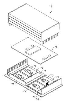
Referring now to figures 7 and 8, there are shown in
detail a power converter module built in accordance with
the present invention. In these figures, the bounding
CA 02261616 1999-O1-21
WO 98/04029 PCT/CA97/00459
22
wires and the details of the low power electronic circuit
boards are omitted to not overload them. Figure 7 is a
disassembled view of the module, and figure 8 is an
assembled view of the same module. Four large power
Mosfet chips 70 with built in free wheel diodes are used
as semiconductor chips. These chips 70 are characterized
by ultra fast turn off speed capability. The insulating
substrate 32 is made of alumina. A multi layer ceramic
capacitor 72 is mounted on top of the assembly. Thereby
l0 the whole assembly forms one half bridge power converter
similar to the one shown in figure 4. Two gate drivers 74
are mounted on conductive plates 76, in close proximity to
the power Mosfets chips 70.
A control board 78, operating with the drivers 74 is
inserted in a gap located underneath the capacitor 72 when
the module is assembled. The control board 78 comprises
digital and analog components such as a micro-controller
with sensors and amplifiers ; digital inputs/outputs to be
linked with a master controller ; and analog outputs to
drive the semiconductor chips via the drivers 74. A
number of conductive links electrically connect the
control board 78 to the drivers 74 so that gate control
signals are provided to the power Mosfets 70 via the
driver 74 and the control board 78. The control board 78
supports the analog and the logic circuit not required on
the ceramic base, thus reducing significantly the size of
the substrate 32. The increase of the gap to insert the
control board 78 has less impact on the stray
interconnection inductance compared to the impact
resulting from an increase of the substrate surface along
direction B. This control board 78 is not shown in the
previous figures to not overload them. The numbers 80 and
82 indicate cross section surfaces that will be referred
to later in the description.
Referring now to Figure 9, there is shown the voltage
measured directly across one row of the Mosfet chips 70
CA 02261616 1999-O1-21
WO 98/04029 PCT/CA97/00459
23
shown in figures 7 and 8 during a turn off sequence of the
current flowing through the Mosfet chips 70. The cutoff
current is at 125 amperes and is coming from an inductive
load while the operating bus voltage is at 400 volts. It
can be observed that the voltage has a spike with a
ringing decay caused by the oscillation of a stray
interconnection inductance L2 that is in series with the
output capacitance of the Mosfet chips supporting the
voltage. The energy contained within the oscillation is
l0 eliminated by joule effect in the resistive links. The
stray interconnection inductance L2 can be evaluated by
means of the damping frequency and a 2nd order equation of
the series resonant LCR circuit. The damped frequency can
be calculated with the following equation .
_ 1
(damped - 1- Z 2 ( 2 ) ,
2n L2C
where z is a damping factor and has a value within the
interval OsZsl. Without evaluating z, we can modify the
equation to get .
1
(damped ~
2n L2C
We can change the equation to .
1
4
L2 s 4II2 C .(damped ( )
The damped frequency of the voltage shown in figure
9 is about 40 Mhz, and the voltage oscillates around 400
volts.
Referring now to figure 10, there is shown, for the
embodiment of figures 7 and 8, the measured output
capacitance versus the voltage withstand by the Mosfet
chips 70 of one row with respect to the substrate 32. At
400 volts, the capacitance is about 1.9 x 10-g Farad. By
calculating the value of the interconnection inductance L2
by means of equation (4), we get .
CA 02261616 1999-O1-21
WO 9$/04029
- 24
.LZ _< 8.3 ~ 10-9 Henry.
PCT/CA97/00459
Referring back to figure 8, the magnetic flux
responsible for the induced voltage spike passes in part
through the cross section 8o between the substrate 32 and
the capacitor 72. The other part of the flux passes
through the cross section 82 in the capacitor 72 and
depends solely on the current change distribution within
the mufti layer geometry of the capacitor. At 40 Mhz, the
skin depth in the capacitor electrodes has a value
l0 comparable to the thickness of one of its electrode plates
so that the total current gradient loop flows in the first
lower layers of the superimposed conductive electrode
plates. Thus, no magnetic flux appears in the upper part
of the capacitor, the magnetic flux passing mostly in the
cross section 80. At high frequencies, any flux change
within the capacitor 30 is cancelled by internal current
loop therefore no high frequency flux change can exist
within the body of capacitor 30.
The cross section 80 of the prototype that has been
confidentially tested is about 5.5 x l0-4 m2 and the length
of the module is about 0.03 metres. A cylindrical current
loop with an equivalent cross section has a diameter equal
to 0.026 metres. Hence the inductance computed with
equation (1} is equal to 16.6 x 10⁻⁹ Henry. The lower
interconnection inductance L2 deduced from the equation
(4) can be attributed to the presence of capacitor 30 and
to the presence of the large aluminum heat sink to which
the module was clamped. For the heat sink, as its
conductive surface reacts with the magnetic field
distribution produced by current gradient loop during the
switching sequence, the flux change in the inductance is
reduced. Consequently, an equivalent stray interconnection
inductance that is lower than what is expected is
obtained.
With the present invention, voltage spike can be
decreased by lowering the stray inductance L2. This is
CA 02261616 1999-O1-21
WO 98/04029 PCT/CA97/00459
achieved by reducing the cross section 80. Unfortunately,
some space has to be allowed for inserting the control
board 78 and to clear the bounding wires 50, 52. But a
further reduction of the voltage spike can be achieved by
5 using a second conductive closed loop that reduces the
flux changes in the stray interconnection inductance. This
second conductive closed loop will be referred to as a
spike killer.
For example, referring now to figure 3, if we place
l0 two conductive walls (not shown) at both ends of the
cylinder, these conductive walls react the same way as
conductive heat sinks would react to the flux density
change coming out from both ends of the cylinder. These
conductive walls would act as conductive loops embracing
15 the flux density coming out at each end. The voltage
produced in the loops is in proportion to the flux
changing rate:
_ _°I~' .
dt
Reacting to the presence of this voltage, a current
20 builds up and immediately generates a magnetic field
change in opposition to the magnetic field source, which
results in reducing the flux change within the loops.
Referring now to figure 11, there is shown an
embodiment based on the above-mentioned principle. The
25 module has conductive walls 21 placed respectively at both
ends of the module. These walls 21 cover at least the
crass section 8o of the module shown in figure 8. Each of
these conductive walls 21 could be connected to one of the
three terminals 20, 22 and 24. The cylindrical current
3o path and the walls at both ends are like two coils with a
mutual coupling that is not perfectly matched due to their
relative position compared to each other so that only a
portion of the flux source fluctuation is reduced.
Referring now to figure 12, there is shown a more
effective way to reduce the voltage spike according to the
CA 02261616 1999-O1-21
WO 98/04029 PCT/CA97100459
26
present invention. The magnetic field H1 generated by the
cylindrical current loop 110 is surrounded by a second
cylindrical conductive loop 1i2. Preferably, the second
loop 112 matches as closely as possible the path followed
by the first current loop 110. With this circuit, any
magnetic field H~ generated by a current I1 produces a ma-
gnetic flux density that is also embraced by the second
cylindrical loop 112. Any change of the cylindrical
current I1 produces a voltage drop within the cylindrical
conductive loop path 112 due to the flux variation. As
the second cylindrical loop 112 is a short-circuit, a
cylindrical current change I2, in opposite direction,
immediately appears in reaction with the presence of the
voltage drop, to produce a magnetic field H2 in opposition
to the magnetic field source H1. This magnetic field H2
reduces the resulting magnetic flux change. As the current
changes I1 and I2 occurs in cylindrical current path that
are almost identical in size and location, the majority of
the flux change generated by the cylindrical current
change I1, is cancelled by the opposite flux change
generated by the cylindrical current change I2, thereby,
killing the voltage spike associated to the flux source
fluctuation.
Referring now to figure 13, there is shown an
electric circuit equivalent to the two concentric
cylindrical loops 110, 112 of figure 12. The loops 110,
112 are represented by a transformer that has its
secondary winding (not shown) shorted. There is a current
source I1 connected in series to a circuit composed of a
mutual inductance M representative of the flux embraced by
the two cylinders 110, 112 plus two very small leakage
inductances L3 and I,~ associated to the leakage flux,
generated by one of the two cylinders 110, 112 and not
embraced by the other, due to improper matching. Also
there are two resistors Rl(f} and R2(f) defining the con-
ductors resistance at a rated frequency in relation to the
CA 02261616 1999-O1-21
WO 98104029 PCT/CA97/00459
27
skin effect. The closer the second cylinder 112 shown in
figure 12 is to the first cylinder 110 shown in figure 12,
the lower the leakage inductances L3 and L4 are.
Referring now to figure 14, there is shown a
perspective view of a module with a second conductive
closed loop in accordance with the present invention. The
module assembly is similar to the one shown in figure 4
except that it further comprises a housing including
conductive walls 90 surrounding the reduced cross section
l0 belt-like current closed loop 64 shown in figure 5,
whereby, in operation, an electric current is magnetically
induced into the conductive walls 90 to further reduce
voltage spikes associated to stray interconnection
inductance. The conductive walls 90 surrounds the module
assembly along direction A. These conductive walls 90 are
insulated from the conductive parts within the module
assembly by an insulating material 91. These conductive
walls 90 form a closed loop which embraces the magnetic
flux density generated by the transient belt-like current
of the half bridge power converter during the switching
sequence. Thereby, a counter current is induced in the
closed loop 90 and reduces any flux change within the
cross section thereof. As there is no flux produced in the
capacitor, the matching of the two loops is very good and
consequently two concentric belt currents in opposite
direction are produced. In doing so, the flux change in
the stray interconnection inductance of the module is
significantly reduced, and therefore voltage spikes are
also reduced. According to the preferred embodiment shown
in figure 14, the method for converting a DC voltage into
an AC voltage comprises the additional step of surrounding
the reduced cross section belt-like current closed loop by
means of a housing including conductive walls.
The spike killer described above acts like a clamping
device which maintains constant most of the magnetic field
produced in the belt-like current closed loop 64 shown in
CA 02261616 1999-O1-21
WO 98/04029 PCT/CA97/00459
28
figure 5 during the switching operation. The energy
contained in the magnetic field is stored in the mutual
stray inductance M that has a value near to the stray
inductance L2 shown in figure 1.
Referring now to figure 15, there is shown a circuit
diagram representative of a power converter including the
module shown in figure 14, assuming that there is a
sufficient good matching between the two closed loops to
neglect leakage inductances L3 and L4 shown in figure 13.
The current distribution can be represented by tour mesh
currents I1, I2 , I Loads and ISource ~ The mesh currents ILoad
and Isource are continuous and thus do not produce
significant current discontinuity. A high flux change is
generated by changes in mesh currents I1 and I2. This high
flux is dependent upon the geometry of path of currents I1
and I2.
Ref erring now to figures 16 ( a } , ( b ) and ( c ) , there
are shown curves illustrating the AC mesh currents I1 and
I2 of figure 15 with respect to time. Mesh current I2 is
shown for two different switching periods T such as
T«M/R(f) and T»M/R(f). As shown in these figures 16(a),
{b) and (c), the spike killer reacts to any flux change by
producing a current that suppresses this flux change
during the switching phase. On a larger time frame, the
life time of the flux produced by the spike killer depends
on its time constant M/R(f), the time period between the
switching sequences being T.
When the time period T is much larger than M/R ( f ) ,
the magnetic energy stored by the spike killer vanishes in
3o joule losses within its conductive loop as shown in figure
16(c) combined with figure 16(a). The total amount of
losses in watts equals the product of the amount of
magnetic energy loss between each switching event by the
switching frequency of the switching events. Thus in this
situation, the spike killer acts as a dissipative clamping
device.
CA 02261616 1999-O1-21
WO 98/04029 PCT/CA97/00459
29
When the time period T is much smaller than M/R(f),
the major portion of the magnetic energy stored in the
spike killer is still present at the beginning of the next
switching phase as shown in figures 16(a) and (b). Thereby
the losses relative to the magnetic energy in Joule in the
spike killer do not increase anymore linearly with the
switching frequency because the magnetic energy is rather
exchange between the mesh currents I1 and I2. Thus in this
situation the spike killer acts as an inductance reducer
l0 that further lowers the mutual stray inductance M of the
power converter module.
Compared to the traditional dissipative clamping
devices, the spike killer of the present invention limits
its power losses as the switching frequency increases.
Also, the spike killer acts directly on the stray
interconnection inductance to maintain the presence of the
stored magnetic energy during the switching phases.
Therefore, no energy is pumped out from the DC supply
source because of this inductance as it is in cases where
2o a traditional clamping device is used, and the current
falling rate is still under the control of the switch.
These are further advantages of the present invention in
relation to the prior art.
The spike killer can be carried out according to the
present invention by closing both ends of the first or
second belt-like current closed loop with conductive
walls. However, this has no meaningful spike killing
effect. A more efficient spike killing effect is achieved
by having two concentric belt-like current closed loops
that are as close as possible with each other without
being in contact to minimize the leakage flux generated by
the first belt like current loop and not embraced by the
second belt like conductive loop. Thereby the use of a
thin insulating material 91, as shown in figure 14, gives
good results. Both open ends can serve as passage for the
electrical and logical cable links. Also, the conductive
CA 02261616 1999-O1-21
WO 98/04029 PCT/CA97/00459
walls of the spike killer could be part of the module
housing which can serve as a heat exchanger. With the use
of a spike killer according to the present invention, flux
fluctuations within the mutual inductance M are reduced to
5 minimum to further reduce the voltage spikes, allow a much
higher switching speed, avoid the use of clamping devices
or snubbers, allow a control of the current falling rate
by the semiconductor switches, allow several switching
devices to be mounted in parallel, limit losses related to
l0 the mutual stray interconnection inductance for high
switching frequency, and reduce the size of the converter.
Referring again to figure 14, for the above reasons,
the power converting module is therefore provided with a
spike killer, according to the present invention. The
15 housing includes the conductive walls 90 surrounding the
4
reduced cross section belt-like current closed loop,
whereby, in operation, an electric current is magnetically
induced into the conductive walls 90 to reduce the flux
change within the mutual stray interconnection inductance.
20 Accordingly, the method of converting a DC voltage into an
AC voltage comprises in this case the additional step of
surrounding the reduced cross section belt-like current
closed loop by means of a housing including conductive
walls 90.
25 The module assembly shown in figure 14 is similar to
the one shown in figure 4 but it further comprises the
conductive walls 90 extending along direction A. These
conductive walls 90 are insulated from the conductive
parts within the module assembly by the insulating
30 material 91. These conductive walls 90 form a closed loop
which embraces the magnetic field generated by the
transient belt-like current of the half bridge power
converter during the switching sequence. Hence, the
conductive walls 90 reacts and induces an opposite
magnetic field which reduces the amplitude of the magnetic
flux change generated in the module, thereby reducing the
CA 02261616 1999-O1-21
WO 98/04029 PCTlCA97/00459
31
voltage spike generated by the mutual stray
interconnection inductance M. With this assembly, a
resulting mutual stray interconnection inductance M that
is lower than the one of prior art, or equal to the one of
embodiment of figures 4, 5 and 6 is obtained. This lower
mutual stray interconnection inductance reduces the
voltage spike, allows a much higher switching speed,
avoids the use of clamping devices or snubbers, allows a
control of the current falling rate by the semiconductor
switches, allows several switching devices to be mounted
in parallel, limits losses related to the mutual stray
interconnection inductance for high switching frequency,
and reduces the size of the converter.
Referring now to figures 17 and 18, there are shown
in detail the same converting module as shown in figure 7
and 8 with a spike killer built in accordance with the
present invention. Figure 17 is a disassembled view of the
module with the spike killer, and figure 18 is an
assembled view of the same module. The module base 32 is
mounted on a copper plate 94 and a cover 96 is bolted on
the copper plate 94. This cover 96 and the copper plate 94
form a second belt-like conductive path around the first
belt-like conductive path in a concentric fashion as shown
in figure 12. The conductive walls of the housing are
then made of at least two parts connected together, which
are the cover 96 and the copper plate 94. Connectors (not
shown) for receiving voltage from the bus DC voltage
source and for supplying the modulated phase are located
in the open ends of the module. Small openings can be
performed on the conductive walls of the belt-like
conductive paths for electrical connections with terminals
within the module without affecting noticeably the
reducing effect on the flux change in the mutual stray
interconnection inductance.
Referring now to figure 19, there is shown the
voltage measured directly across one row of the Mosfet
CA 02261616 1999-O1-21
WO 98/04029 PCT/CA97/00459
32
chips 70 of the embodiment shown in figures 17 and 18
during a turn-off sequence of the current flowing through
the Mosfet chips 70. We can compare figure 9 with figure
19 and see that in figure 19 the cutoff current is also
125 amperes and is coming from the same inductive load
with the bus voltage also at 400 volts. The voltage
oscillation seen in figure 9 is practically gone and the
voltage spike is reduced, therefore showing the advantage
of the addition of the second belt-like conductive path.
Referring now to figures 20 and 21, there are shown
a larger module that is built with IGBT chips 100 and
diode chips 102. In these figures, the bounding wires and
the details of the circuit boards are omitted to not
overload them. Figure 20 is a disassembled view of the
module, and figure 21 is an assembled view of the same
module. The assembly has a length that is three times
longer along the direction A than the length of the
embodiment shown in figures 17 and 18. The insulating gap
between the second belt-like conductive path and the first
belt-like conductive path, and the gap between the base
plate and the decoupling means are reduced with respect to
the embodiment shown in figures 17 and 18. Eight IGBT
chips with eight diode chips are connected in parallel for
each row of the module. With this assembly, the mutual
stray interconnection inductance is smaller due to the
larger 1/d ratio of the module as shown in equation (1),
1 and d of the module being defined as shown in figure 3.
Referring now to figure 22, there is shown the result
of switching tests performed on the module shown in
figures 20 and 21. The voltage is measured across one row
of IGBT chips 100 during a switching test. The cutoff
current is 45 amps and the bus voltage is set at 500
volts. The test shows a turn off sequence with no
apparent voltage spike and the voltage swings from o to
500 volts in less than 20 nsec. The improvement is due to
the larger 1/d ratio, the smaller insulating gap between
CA 02261616 1999-O1-21
WO 98104029 PCT/CA97100459
33
the two belt-like conductive paths, and the smaller gap
between the base plate and the decoupling means which
further reduce the voltage spike generated in the stray
interconnection inductance as compared to the embodiment
of figures 17 and 18, thereby illustrating the efficiency
of the present invention.
The spike killer of the present invention can be made
according to different embodiments. The modules shown in
figures 17, 18, 20 and 21 illustrate a belt-like
conductive loop having two parts. The first part is the
cover 96 which is made of conductive material, such as
copper or aluminum. This cover 96 has two sides welded or
clamped with securing elements, such as bolts, to the
conductive base plate 94 placed underneath the module
insulating base 32. The plate 94 constitutes the second
part of the loop. The base plate 94 can form a heat
exchanger or can be bounded underneath of the insulating
plate 32, such as a copper bound layout bounded underneath
a copper-ceramic-copper board. Also, to insure proper
insulation, the spike killer is separated from the module
with insulating material, (not shown).
According to the present invention, a spike killer
can be also made by using a thin film metal deposition.
The conductive walls 90 of the housing shown in figure 14
are then formed by a metal deposition over insulating
walls 91. In such a case, the module is first encapsulated
in a plastic or any other material with insulating
properties and is then sprayed with a metallic vapor or
dipped in a liquid metal bath to form a thin film metal
deposit on its surface. This metal deposit forms the belt-
like conductive loop of the spike killer. The thin film
deposit may be only applied on specified portions of the
module such as for example, the top and the sides thereof,
the remaining part of the belt-like conductive loop being
a copper layout bounded underneath the surface of the
insulating base 32.
CA 02261616 1999-O1-21
WO 98104029 PCTICA97100459
34
Referring now to figure 23, there is a schematic
circuit diagram representing a power converter including
the module shown in figure 14. A problem often occurs
because of the stray capacitance present between the load
and an adjacent conductive part such as, for example, the
stray capacitance present between the stator coils of a
motor and its metal hollow portion. This problem is
schematized in the diagram of figure 23. A half bridge
power converter 121 supplies AC voltage to a load 120
having a stray capacitance 122 with a conductive part 124.
Through this stray capacitance 122, the potential of the
conductive part 124, by reference to the electrodes 126
and 128 of the DC bus voltage, oscillates at a frequency
in accordance with the square wave voltage applied to the
load 120 by the half bridge power converter 121. Any form
of stray impedance connected between the load housing and
one of the electrodes 126, 128 of the DC supply voltage
bus produces a current through the stray capacitance 122.
This current is a source of noise problems and may be
harmful.
In a case where none of the electrodes 126, 128 of
the voltage bus is directly grounded to the conductive
part 124, a bypass capacitor 130 with a higher value than
the one of the stray capacitor 122 is connected between
the conductive part 124 and at least one of the bus
voltage electrodes, for instance the electrode 128. The
induced stray current within the stray capacitance 122
follows an easy path through the capacitor 130 back to the
bus electrode 128. With this circuit, the amplitude of the
voltage that builds up on the bypass capacitor 130 is a
fraction of the supply voltage, the value of this fraction
being determined by the ratio of the stray capacitor value
with respect to the bypass capacitor value. In the case of
the module without the spike killer shown in figures 4,5,6
and 11, this bypass capacitor can have one end connected
to one of the electrode terminals 20 or 22 of the module.
CA 02261616 1999-O1-21
WO 98/04029 PCT/CA97100459
The free end of the capacitor is available for connection
with a conductive part producing a stray capacitance with
the load (not shown).
Referring now to figure 24, there is shown an
5 embodiment similar with the one shown in figure 14, but it
further includes a built-in bypass capacitor. In the case
of this module provided with a spike killer according to
the present invention, the free end of the capacitor is
connected to the walls 90 of the belt-like conductive loop
10 of the spike killer, and a free connection point 138 of
the spike killer is available on the conductive loop for
connection to a conductive part (not shown) that forms a
stray capacitance with the load. If this capacitor is a
discrete part, it can be inserted in a space located
15 between the conductive walls 90 of the spike killer and
the module.
In the case of the module shown in figure 24, a
horizontal conductive plate 134 is superimposed over the
top last conductive plate 132 of the superimposed
20 electrode plates 31, and separated therefrom by a
dielectric material 136, such as ceramic, the whole
thereby forming said built-in bypass capacitor. The
conductive plate 134 constitutes one segment of the belt-
like conductive walls 90 of the spike killer. In figure
25 24, for purpose of clarity, the gap shown in this figure
between the plate 134 and the last plate 132 is larger
than the existing gap which is actually the same as the
one between adjacent plates of the superimposed electrode
plates 31. Also, the connection point 138 can be located
30 anywhere on the conductive walls 90 of the spike killer
for connection with the conductive part 124. The capacitor
is connected between the conductive plate 134 which is
part of the conductive walls 90 of the housing, and the
conductive plate 132 which is electrically connected to
35 one of the DC terminals. The conductive walls provide one
connecting point 138 for electrical connection purpose.
CA 02261616 1999-O1-21
WO 98/04029 PCTICA97/00459
36
The capacitor is then formed by a wall of the conductive
walls that is adjacent to the top electrode plate 132 and
that is separated from the top electrode plate 132 by
means of dielectric material 136. Thereby, when the belt-
s like conductive walls of the spike killer are connected to
a conductive part (not shown} forming a stray capacitor
with the load, a bypass capacitor made according to the
present invention is provided.
According to another aspect of the present invention,
to the fact that the module has a very low stray
interconnection inductance which is further clamped by the
spike killer, does not produce a Miller effect (reference:
International Rectifier, Hexfet, Power MOSFET designer's
Manual, application note #947) during the switching phase.
15 This Miller effect is present in gate capacitance
transistors such as Mosfets and IGBTs. In the case of a
Mosfet, the drain current is controlled by the amount of
charges cumulated in its gate to source capacitance.
During the turn-on phase, the drain voltage falls because
20 the increasing drain current induces a voltage across the
interconnection inductance. As the drain voltage falls, a
portion of the gate input charging current is bypassed
through the gate to drain stray capacitance, depriving the
gate to source capacitance of the charges it would have
25 normally received. This negative feedback slows the rising
drain current and is called the Miller effect.
In the case of the module made according to the
present invention, the voltage drop at the interconnection
inductance is negligible so that the Miller effect is not
30 present. Without the Miller effect, the input gate current
is not bypassed and serves only to charge the gate to
source capacitance of the Mosfet or IGBT. Therefore, the
drain current rising rate depends only on the input gate
charging current. When the input gate current is too
35 large, the rising time of the drain or collector current
is very short. This can result in a problem if the switch
CA 02261616 1999-O1-21
WO 98104029 PCT/CA97100459
37
that is turned on takes over the current of an inductive
load that flows, in a free wheel mode, through a diode
having a reverse recovery charge. A high current rising
rate increases the reverse recovery current density within
the diode and the Mosfet or IGBT, which can be destructive
for the semiconductors. To insure a safe operation, the
gate input charging current is limited with a resistor to
limit the rising current rate. After recovery of the
diode, the drain voltage falling~rate is dependent on the
same input gate current now discharging the gate to drain
capacitance. This drain voltage falling rate is less
problematic and can be accelerated to minimize switching
losses. This is carried out by injecting a higher gate
input current to improve the switching performance.
Referring now to figure 25, there is shown a circuit
diagram of a switch with its driver. To improve the
overall switching performance of the switch, during the
turn-on phase, the gate input current is limited to two
values, one for the rising current and one for the falling
voltage. This function is performed by means of the
driver . The driver includes a terminal 220 to receive a
gate signal for the corresponding semiconductor device.
A first resistor R1 is connected between the terminal 220
and the gate 222 of the corresponding semiconductor device
224.
There is a circuit segment including a voltage gate
controlled switch T1 and a second resistor R2 connected in
series. The circuit is connected in parallel to the first
resistor R1. A capacitor C1 is connected between the gate
226 of the voltage gate controlled switch T1 and the
collector 228 of the corresponding semiconductor device
224 for monitoring collector voltage signal thereof. There
is a voltage clamping device X1 connected between the gate
226 of the voltage gate controlled switch T1 and the
terminal 220. Whereby, in operation, the first resistor
R1 limits gate current of the corresponding semiconductor
CA 02261616 1999-O1-21
WO 98/04029 PCT/CA97/00459
38
device prior to a drop of the collector voltage signal
thereby limiting rise time of the collector current, and
the first and second resistors R1 and R2 limit the gate
current of the corresponding semiconductor device 224
during the drop of the collector voltage thereby limiting
dropping time of collector voltage.
A first resistor R1 is connected between the input
that receives the square voltage signal and the gate 222
of the switch 224 to limit the gate input charging current
to a first value Igl, until the current flowing through
the diode D evacuates its reverse recovery charges and
enters its blocking state. Then, the drain voltage starts
to fall and is detected by a capacitor C1 connected
between the drain 228 of the switch 224 and the gate 226
of a P channel Mosfet T3 that is connected in series with
a second resistor R2. when the switch 224 is a Mosfet, the
capacitor C1 is connected to the drain 228, and when the
switch 224 is an IGBT, the capacitor is connected to the
collector. In the text when we refer to the collector,
depending on the situation it could also means the drain.
The Mosfet T1 and resistor R2 are both in parallel to re-
sistor R1. The dropping voltage induces a current through
the capacitor C1 which charges rapidly the gate of the P
channel Mosfet T1 which immediately conducts to establish
a series connection with the resistor R2. Thus, the input
current is increased by a second gate input charging
current Ig2, further accentuating the voltage dropping
rate to increase the switching speed, thereby reducing the
switching losses. A clamping means X1 is connected across
the gate capacitance of the P channel Mosfet T1 to limit
the voltage. A capacitor C2 connected in series with a
resistor R3 is added in parallel with the resistor R1, to
inject a current pulse in the gate 222 to shorten the
delay between the input voltage transition and the start
of the drain current rise-up.
Referring now to figure 26, there is shown one of the
CA 02261616 1999-O1-21
WO 98/04029 PCT/CA97/00459
39
possible applications of the present invention. This
application is for motor wheels such as the one disclosed
in the U. S . patent No. 5, 438, 228 . The electric motor is
mounted in a wheel, the power converter of the motor being
mounted in a hollow portion of the wheel. The motor has an
outer rotor 200 and an inner stator 201 supported on an
axle by a cross member 204. The power converter includes
modules 205 and capacitors 206, all mounted on the legs of
the supporting cross member 204. Conductors 207 are
l0 provided to connect each module to a DC voltage bus
provided in the hollow portion, and to connect each module
to the windings of the stator. The modules constitute a
polyphase DC to AC power converter. The compactness of the
modules of the present invention makes them convenient for
installation within the hollow portion of the motor wheel.
Referring now to figure 27, there is shown how the
power converter of the present invention is mounted on the
cross member 204 of the motor wheel. There is the
combination of three power converting modules 205 in a
motor wheel provided with a stator frame supported by a
cross member 204 made of conductive material. The three
modules 205 are mounted respectively on three legs of the
cross member 204 within the motor wheel. The modules 205
form a three-phase power converter which further comprises
a first conductive bus having a pole 209 connected to one
of the DC terminals of each module 205 with a feed-trough
connector 211 on one side of the cross member 204. There
is a second conductive bus having a pole (not shown but
similar to pole 209 with connectors similar to connectors
211) connected the other of the DC terminals of each
module on the other side of the cross member 204. The two
conductive bus delimit spaces between adjacent modules
that are filled with the conductive material of the cross
member 204. The two conductive bus are separated from the
module housing and the cross member 204 by insulating
material 210, whereby, in operation, an electric current
CA 02261616 1999-O1-21
WO 98/04029 PCT/CA97/00459
is magnetically induced in the cross member 204 to
suppress the magnetic flux change generated in the stray
interconnection inductance present between the modules.
The machine is a three-phase permanent magnet AC
5 machine. Three modules 205, each containing one half
bridge power converter, one for each phase, are mounted on
the legs of the cross member 204. There is one module per
leg. Each leg acts as a heat exchanger for the
corresponding module. The bipolar DC voltage bus provided
10 in the hollow portion has one pole 209 connected with
feed-trough connectors 211 to terminal 22 of a module such
as the one shown for example in figure 4. All the
connections are located on one side of the cross member
204. The other pole (not shown but similar to pole 209
15 with connectors similar to the connectors 211) of the DC
voltage bus is connected to the other terminal 20 of the
module of figure 4, all the connections being located on
the other side of the cross member 204. Each pole is
isolated from the conductive part of the cross member and
20 the module housing with an insulating layer 210.
As the three modules 205 are apart, the stray
inductive interconnection linking the modules 205 may
cause a voltage oscillation between each module capacitor
due to the fact that the load current are switched by each
25 module and that this switching alternates from one pole to
the other. In this case, the interconnection inductance
has to be minimized. One known method for minimizing
interconnection inductance is to connect two adjacent
modules by means of two conductive strips mounted side by
30 side and separated with a thin insulating material. To
minimize interconnection inductance with the present
invention, it requires that one interconnection passes
from one side of the module to the other side. Here, a
simpler connection is made by directly linking the modules
35 by means of straight interconnections located alongside
legs of the cross member, as shown in figure 27. With this
CA 02261616 1999-O1-21
WO 98/04029
- 41
PCT/CA97/00459
setup, the volume between two adjacent interconnections
and between two adjacent modules is completely filled with
the conductive material, such as aluminum, of the cross
member 204. Thereby a further spike killing effect is
obtained by suppressing the magnetic flux changes produced
by interconnection inductances present between the
modules, thus, avoiding oscillation of the bus voltage
between the capacitors of each module. The centre of each
leg could be empty of conductive material without
l0 affecting the spike killing effect.
In summary, according to the present invention, the
interconnection inductance of a power converter assembly
is greatly reduced by integrating the power electronics
switching devices, the DC terminals, the AC terminal and
a capacitor within one package characterized with a belt-
like current closed loop. The voltage spike induced in the
interconnection inductance can be further reduced by
adding a second belt-like closed loop, referred here as a
spike killer, which surrounds the module to embrace in the
belt-like transient current loop circulation generated in
the module during a switching event. The reduced
interconnection inductance and the spike killer allows a
higher switching speed and frequency with a lower voltage
spike across the switches thus improving the efficiency of
the power converter.
Although the invention has been described above in
detail within the framework of preferred embodiments, it
should be understood that the scope of the present
invention is to be determined by the appended claims.