Note: Descriptions are shown in the official language in which they were submitted.
CA 02261639 1998-11-24
WO 97/48032 PCT/US97/09367
PROGRAMMABLE METALLIZA JION CELL STRUCTURE
AND METHOD OF MAKING SAME
Technical Field
The present invention relates, generally, to a programmable metallization cell
5 comprising a fast ion conductor, a plurality of electrodes and a voltage-controlled
metal structure or dendrite formed at the surface of the fast ion conductor between
the electrodes, and more particularly, to devices such as electronic memory,
programmable resistors and capacitors, integrated optical devices, and sensors
utilizing the programmable metallization cell.
0 Background Art and Tc~, Jical Pro~ole "s
Memory Devices
Memory devices are used in electronic systems and computers to store
information in the form of binary data. These memory devices may be characterized
into various types, each type having associated with it various advantages and
1 5 disadvan~ages.
For example, random access memory ~"RAM") which may be found in personal
computers is volatile semiconductor memory; in other words, the stored data is lost
if the power source is disconnected or removed. Dynamic RAM ("DRAM") is
particularly volatile in that it must be "refreshed" ~i.e. recharged) every few
20 microseconds in order to maintain the stored data. Static RAM ("SRAM") will hold
the data after one writing so long as the power source is maintained; once the power
source is disconnected, however, the data is lost. Thus, in these volatile memory
configurations, information is only retained so long as the power to the system is not
turned off.
CD-ROM is an example of non-volatile memory. CD-ROM is large enough to
~ contain lengthy audio and video segments; however, information can only be read
CA 02261639 1998-11-24
W O 97148032 PCTAJS97/09367
from and not written to this memory. Thus, once a CD-ROM is programmed during
manufacture, it cannot be reprogrammed with new information.
Other storage devices such as magnetic storage devices (i.e., floppy disks, harddisks and magnetic tape) as well as other systems, such as optical disks, are non-
5 volatile, have extremely high capacity, and can be rewritten many times.
Unfortunately, these memory devices are physically large, are shock/vibration-
sensitive, require expensive mechanical drives as well as consume relatively large
amounts of power. These negative aspects make these memory devices non-ideal
for low power portable applications such as lap-top and palm-top computers and
1 0 personal digital assistants ("PDAs") .
Due to the rapidly growing numbers of compact, low-power portable computer
systems in which stored information changes regularly, read/write semiconductor
memories have become widespread. Furthermore, because these portable systems
require data storage when the power is turned off, a non-volatile storage device is
1~ required. The simplest programmable semiconductor non-volatile memory devices in
these computers are programmable read-only memory ("PROM"). The most basic
PROM uses an array of fusible links; once programmed, a PROM cannot be
reprogrammed. This is an example of a write-once read-many ("WORMn) memory.
The erasable PROM IUEPROM'') is alterable, but each rewrite must be preceded by an
20 erase step involving exposure to ultra violet light. The electrically erasable PROM
~"EEPROM" or "E2PROM") is perhaps the most ideal of conventional non-volatile
semiconductor memory, as it can be written to many times. Flash memories, another
type of EEPROM, have higher capacity than the low density, traditional EEPROMs but
lack their endurance. One major problem with EEPROMs is that they are inherently25 complex. The floating gate storage elements that are used in these memory devices
are difficult to manufacture and consume a relatively large amount of semiconductor
real estate. Furthermore, the circuit design must withstand the high voltages
necessary to program the device. This means that an EEPROM's cost per bit of
memory capacity is extremely high compared with other means of data storage.
CA 02261639 1998-11-24
WO 97/48032 PCT/US97109367
Another disadvantage of EEPROMs is that although they can retain data without
having the power source connected, they require relatively large amounts of power
to program. This power drain can be considerable in a compact portable system
powered by a battery.
Recently, a great amount of attention has been given to an alternative non-
volatile memory technology based on ferroelectric materials. Unfortunately, there is
still a great number of problems associated with this data storage approach that have
prevented the widespread application of ferroelectric materials, the various problems
including non-ideal storage characteristics and extreme difficulties in manufacturing.
Accordingly, in view of the various problems associated with conventional data
storage devices described above, it is highly desirable to have a read/write memory
technology and device which is inherently simple and inexpensive to produce.
Furthermore, this memory technology should meet the requirements of the new
generation of portable computer devices by operating under a low voltage while
15 providing high storage density, non-volatility, and a low manufacturing cost. Programmable Passive and Active Components
Electronic circuits may comprise literally millions of component parts. These
component parts generally fall into two distinct categories, namely, passive
components and active components. Passive components, such as resistors and
20 capacitors, have electrical values associated with them which are relatively constant.
On the other hand, the electrical values of active components, such as transistors,
are designed to change when a voltage or current is applied to control electrodes.
Because of the extensive use of these two types of components, it is highly
desirable to have a low-cost device which may perform both the functions of a
25 passive component and an active component. For example, it would be highly
desirable to have a device that acts as an active component which responds to anapplied signal by altering its resistance and capacitance and yet, in an alternate
~ embodiment, the same device acts as a passive component which can be pre-
programmed (i.e., the change is "remembered" by the device after programming is
.
CA 02261639 1998-11-24
WO 97/48032 PCT/US97109367
complete). Such a device would be able to be implemented in many diverse
applications from tuned circuits in communications equipment to volume controls in
audio systems.
Optical Devices
Recently, there has been an enormous demand for various optical devices such
as display devices for lap-top computers, high definition television ("HDTV"), spatial
light modulators, and the like. It would be highly desirable to have a low cost, highly
manufacturable device that may be utilized in such optical devices as, for example,
a shutter to block the passage of light through an optical cell or as a mirror which
10 may deflect a scanned incident beam on or off a screen or other target.
Sensors
The measurement of exposure to ultraviolet radiation and other forms of
radiation is very important as radiation is believed, for example, to promote skin
cancer and other damaging effects to an individual.
Accordingly, it is desirable to have a highly manufacturable device that may be
used in low-cost, wavelength sensors or sensor arrays for short wavelength radiation
such as ultraviolet radiation ~10-7-10-9 meters), x-rays (10-9-10-1'), and gamma rays
(1 0-'1-1 o-14).
Conclusion
Because of the widespread use of devices such as memory devices,
programmable resistor and capacitor devices, electro-optical devices, and sensors, it
is very desirable to have a low cost, easy to manufacture device that may be
implemented in all of these various applications, among others.
Su""".,r~ of the Inv~.,t;~ n
In accordance with an exemplary embodiment of the present invention, a
programmable metallization cell ("PMC") comprises a fast ion conductor such as achalcogenide-metal ion and at least two electrodes (e.g., an anode and a cathode)
comprising an electrically conducting material and disposed at the surface of the fast
CA 02261639 1998-11-24
W O 97/48032 PCTrUSg7/09367
ion conductor a set distance apart from each other. Chalcogenide materials as
referred to herein include all those compounds involving sulfur, selenium and/ortellurium. In a preferred embodiment, the fast ion conductor comprises a
chalcogenide and Group I or Group ll metals ~most preferably, arsenic trisulphide-
5 silver), the anode comprises silver and the cathode comprises aluminum or otherconducting material. When a voltage is applied to the anode and the cathode, a non-
volatile metal dendrite rapidly grows from the cathode along the surface of the fast
ion conductor towards the anode. The growth rate of the dendrite is a function of
the applied voltage and time; the growth of the dendrite may be stopped by removing
10 the voltage or the dendrite may be retracted back towards the cathode by reversing
the voltage polarity at the anode and cathode. Changes in the length of the dendrite
affect the resistance and capacitance of the PMC.
In accordance with one aspect of the present invention, a PMC is utilized as a
memory storage device. More particularly, by applying a constant or pulsed bias to
15 the cathode and anode over a period of time, a dendrite of a certain length is
produced. ~ssociated with this dendrite length are measurable electrical parameters
such as resistance and capacitance. In a preferred embodiment, both analog or digital
values may be stored in the device.
In accordance with another aspect of the present invention, a PMC is employed
20 as a programmable resistorlcapacitor device wherein a specific resistance or
capacitance value is programmed by applying a DC voltage for an appropriate period
of time.
In accordance with yet another aspect of the present invention, an electro-
optical device comprises a PMC having electrodes of broad width. When a large
25 voltage is applied to the electrodes, a dendrite "sheet" is produced that acts as a
shutter to block the passage of light through an optical cell or as a mirror fordeflecting a scanned incident beam on or off a screen or other target.
In accordance with still a further aspect of the present invention, a PMC is
utilized as a short wavelength radiation sensor. Because the growth and dissolution
CA 02261639 1998-11-24
W O 97/48032 PCT~US97/09367
rate of the metal dendrite is sensitive to certain wavelengths, the difference in the
growth rate of the dendrite can than be related to the intensity of the incidentradiation .
Brief Descr"~ n of the Drawing Figures
The present invention will hereinafter be described in conjunction with the
appended drawing figures, wherein:
FIG. 1 A is a plan view of a programmable metallization cell in a lateral
configuration in accordance with one embodiment of the present invention;
FIG. 1 B is a cross-sectional view of FIG. 1 A taken from line 1-1;
FIG. 2 is a graphic representation showing the relationship between resistance
and time in an exemplary programmable metallization cell;
FIG. 3 is a graphic representation showing the relationship between capacitance
and time in an exemplary configuration of a programmable metallization cell;
FIG. 4A is a plan view of a programmable metallization cell in a vertical
15 configuration in accordance with another embodiment of the present invention;FIG. 4B is a cross-sectional view of FIG. 4A taken from line 2-2;
FIG. 5A is a plan view of an exemplary lateral type memory device in
accordance with the present invention;
FIG. 5B is a cross-sectional view of FIG. 5A taken from line 5-5;
FIG. 5C is a cross-sectional view of a lateral memory device in accordance with
another embodiment of the present invention;
FIG. 5D is a cross-sectional view of a lateral memory device in accordance with
yet another embodiment of the present invention;
FIG. 5E is a cross-sectional view of a lateral memory device in accordance with
25 still yet another embodiment of the present invention;
FIG. 6A is a plan view of an exemplary vertical-type memory device in
accordance with the present invention;
FIG. 6B is a cross-sectional view of FIG. 6A taken from line 6-6;
, CA 02261639 1998-11-24
P~TIUS 97/ 093b7
106Rec'dPCTlPTC 18 DEe l~l
FIG. 7A is a plan view of an exemplary embodiment of a programmable
resistance/capacitance device in accordance with the present invention;
FIG. 7B is cross-sectional view of FIG. 7A taken from line 7-7;
FIG. 8A is a plan view of a programmable resistance/capacitance device in
5 accordance with another embodiment of the present invention;
FIG. 8B is a cross-sectional view of FIG. 8A taken from line 8-8;
FIG. 9A is a plan view of an exemplary electro-optical device in accordance
with the present invention;
FIG. 9B is a cross-sectional view of the electro-optical device of FIG. 9A taken10 from line 9-9;
-~ FIG. 1 OA is a plan view of an exemplary radiation sensor in accordance with
the present invention; and
FIG. 1 OB is a cross-sectional view of the sensor of FIG. 1 OA taken from line
10-10.
15 Detailed ~es~ript;D ~ of r~f~ J Exemplary Embodiments
1. Programmable Metallization Cell
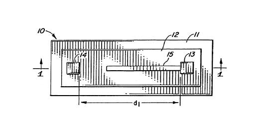
Referring now to FIGS. 1 A and 1 B, an exemplary programmable metallization
cell ("PMCn) 10 in a lateral or horizontal configuration is shown in accordance with
~ ,. .
one embodiment of the present invention. FIG. 1 A is a plan view of PMC 10 and FIG.
20 1B is a cross-sectional view of PMC 10 taken from line 1-1 of FIG 1A. PMC 10
comprises a fast ion conductor 12 and a plurality of electrodes 13 and 14 (e.g.,cathode 1 3 and anode 14) disposed at the surface of fast ion conductor 1 2.
Optionally, a supporting substrate 11 may be provided at the base of fast ion
conductor 12, above electrodes 13 and 14 (not shown), or both, to give added
25 strength and rigidity to device 10. Substrate 11 may appropriately comprise, for
example, plastic, glass, or semiconductor material.
With continued reference to FIGS. 1 A and 1 B, fast ion conductor 12 comprises
a solid electrolyte, a metal ion-containing glass, a metal ion-containing amorphous
AMENDED StlEE~
CA 02261639 1998-11-24
W O 97/48032 PCTrUS97109367
semiconductor, a chalcogenide-metal ion, or the like. In the broadest sense, a
chalcogenide material in accordance with the present invention includes any
compound containing sulfur, selenium and/or tellurium, whether ternary, quaternary
or higher compounds. In a preferred embodiment, fast ion conductor 12 comprises
5 a chalcogenide-metal ion composition, the chalcogenide material is selected from the
group consisting of arsenic, germanium, selenium, tellurium, bismuth, nickel, sulfur,
polonium and zinc (preferably, arsenic sulphide, germanium sulfide, or germaniumselenide) and the metal comprises various Group I or Group ll metals tpreferably,
silver, copper, zinc or a combination thereof). The chalcogenide-metal ion
10 composition may be obtained by photodissolution, by depositing from a source
comprising the chalcogenide and metal, or by other methods known in the art.
With continued reference to FIGS. 1 A and 1 B, in a most preferred embodiment,
fast ion conductor 12 comprises arsenic trisulphide-silver (''AszS3-Ag''). The silver is
introduced into the As2S3 by illuminating a thin silver film and the As2S3 layer with
15 light of wavelength less than 500 nanometers. If sufficient silver is present, the
process results in the formation of a ternary compound which is stoichiometrically
similar to the mineral smithite (AgAsS2), a stable amorphous material. Preferably,
sufficient silver is deposited on the chalcogenide surface to form the equilibrium
phase throughout the chalcogenide layer. While it is possible for PMC 10 to operate
20 without fast ion conductor 12 being in the equilibrium phase, the operation of PMC
10 requires considerably higher voltage.
With continued reference to FIGS. 1A and 1B, electrodes 13 and 14 are
suitably arranged apart from each other at the surface of fast ion conductor 12,forming a distance dl in the range of preferably hundreds of microns to hundredths
25 of microns. Electrodes 13 and 14 may comprise any electrically conducting material
that will produce an electric field for the rapid transport of metal ions in fast ion
conductor 12. When a voltage is applied to electrodes 13 and 14, a metal dendrite
15 grows from electrode 13 (i.e. cathode), the electrode connected to the negative
pole of the power supply. Dendrite 15 grows by precipitation from the soiid solution
- 8 -
CA 02261639 1998-11-24
WO 97t48032 PCT/US97109367
of cations ~e.g. silver cationst on cathode 13 created by a high local electric field.
Dendrite 15 may be allowed to grow across the surface of fast ion conductor 12 until
it meets opposing electrode 14, thereby closing the gap and completing the electrical
circuit. Alternatively, dendrite 15 may be halted before it reaches anode 14 by
5 removing the voltage source or by placing an insulating physical barrier before the
anode. As long as dendrite 15 does not touch opposite electrode 14, its growth can
be easily stopped and retracted by reversing the voltage at electrodes 13 and 14.
Changes in the length of dendrite 15 affect the resistance and capacitance of PMC
10; these changes may then be easily detected using simple circuitry known in the
10 art. Another important characteristic of dendrite 1 5 is its non-volatility; metal
dendrite 1 5 remains intact when the voltage is removed from electrodes 13 and 14.
With continued reference to FIGS. 1 A and 1 B, in a preferred embodiment where
fast ion conductor 12 comprises As2S3-Ag, anode 14 comprises silver such as a solid
silver layer or a silver-aluminum bilayer; this allows for rapid dendrite growth to occur
15 at a relatively low electric field as anode 14 acts as a sacrificial electrode. Cathode
13 may be a solid silver layer, an aluminum layer, or a silver-aluminum bilayer, and
in some configurations aluminum is the preferred material. If electrodes 13 and 14
comprise silver (e.g. pure silver or an aluminum-silver bilayer), dendrite 15 will grow
from the electrode that is connected to the negative side of the power supply; when
20 the voltage is reversed, the previous dendrite is dissolved or retracted and a new
dendrite grows from the opposite electrode. Alternatively, if cathode 13 comprises
aluminum and anode 14 comprises pure silver or a silver-aluminum bilayer, dendrite
15 will only grow from cathode 13; when the voltage polarity is reversed, dendrite
15 will retract towards cathode 13 but little or no dendrite growth will occur from
25 opposite electrode 14. If anode 14 or both cathode 13 and anode 14 comprise
aluminum or another non-dissolving metal (e.g., gold), growth of dendrite 15 becomes
extremely slow and requires a high applied voltage.
With continued reference to FIGS. 1 A and 1 B, the growth rate of dendrite 15
is a function of the applied voltage and time. Low voltages result in relatively slow
g
CA 0226l639 l998-ll-24
W O 97/48032 PCTAJS97/09367
growth whereas higher voltages produce extremely rapid growth. In small geometrydevices (i.e., a few microns in width), voltages in the range of approximately 0.5
volts to 1.0 volts produce single dendrite structures with growth rates greater than
10-3 mts while voltages in excess of 10 volts can produce a "sheetn of dendrite 15
5 between electrodes 13 and 14, rather than a single dendrite.
With continued reference to FIGS. 1A and 1 B, a soft, polymeric coating (not
shown) such as polyimide or novolac may be disposed over fast ion conductor 12 and
electrodes 13 and 14 for protecting PMC 10 from moisture or physical damage while
still allowing growth of dendrite 15.
Referring now to FIGS. 2 and 3, graphic representations show the relationship
in a PMC between resistance and time and capacitance and time, respectively. ThePMC used to obtain these results was a relatively large device (i.e. approximately 12
microns from electrode to electrode); nevertheless, these results provide a fairoverview of the general electrical characteristics of the PMC.
With specific reference to FIG. 2, a curve 32 represents the relationship
between the resistance and time of the PMC. Before any voltage is applied to theelectrodes of the PMC, the resistance of the PMC is approximately 2.65 megohms.
When a small 0.7 volt bias is applied to the electrodes as a series of 0.5 second
pulses, the resistance of the PMC demonstrates an inversely proportional relationship
20 to the length of time the voltage is applied to the electrodes. For example, the
resistance value after 4.5 seconds of applied voltage has decreased approximately
550K ohms to approximately 2.1 megohms. Greater changes in the resistance value
are achieved when a smaller PMC device or larger voltages are used.
With reference now to FIG. 3, a curve 42 shows the relationship between the
25 capacitance of the PMC versus time. At approximately 0.5 seconds of an applied 0.7
volt bias, there is approximately 0.45 picofarads of capacitance for the PMC device.
When 0.7 volts is applied to the electrodes as a series of 0.5 second pulses, the
capacitance of the PMC then rapidly increases to approximately 0.9 picofarads after
- 10-
CA 02261639 1998-11-24
WO 97/48032 PCT/US97/09367
4.5 seconds. The capacitance increase is even greater if a smaller PMC device isused or larger voltages applied.
With reference now to FIGS. 4A and 4B, a vertically configured PMC 20 is
illustrated in accordance with another embodiment of the present invention. While
5 the lateral configuration of FIGS. 1 A and 1 B is easier to fabricate and has a lower
associated manufacturing cost, the vertical configuration provides the advantages of
a much more compact device. FIG. 4A is a plan view of PMC 20 in the vertical
configuration and FIG. 4B is a cross-sectional view of PMC 20 taken from line 2-2 of
FIG 4A.
With continued reference to FIGS. 4A and 4B, an electrode 23 (e.g., a cathode)
and an electrode 24 (e.g., an anode~ are positioned apart from each other in parallel
planes. A fast ion conductor 22 is disposed or sandwiched between electrodes 23
and 24. When a voltage is applied to cathode 23, a dendrite 25 grows from cathode
23 along the surface of fast ion conductor 22 towards anode 24. In a preferred
embodiment, a supporting substrate 21 is provided adjacent electrode 24 or 23 tosupport and give rigidity to PMC 20.
Il. Metal Dendrite Memory
As described above, a PMC may be implemented in various different
technologies. One such application is in memory devices.
Turning now to FIGS. 5A and 5B, an exemplary memory cell or metal dendrite
memory ("MDM") cell 50 is shown in a lateral or horizontal configuration. FIG. 5A
is a plan view of MDM 50 and FIG. 5B is a cross-sectional view of MDM 50 taken
from line 5-5 of FIG 5A. In this illustrated embodiment, MDM 50 comprises a
substrate 51 which provides the physical support for the memory cell or device. If
25 substrate 51 is non-insulating or otherwise incompatible with the materials used in
MDM 50, an insulator 56 may be disposed on substrate 51 to isolate the active
portion of MDM 50 from substrate 51. Next, a fast ion conductor 52 is formed on
substrate 51 (or insulating layer 56 if an insulator is used). Fast ion conductor 52 is
CA 02261639 1998-11-24
WO 97/48032 PCTIUS97/09367
appropriately patterned to provide isolation from memory cells or devices which may
be adjacent to cell 50. The dimensions (e.g. Iength, width and thickness) of fast ion
conductor 52 will determine, in part, the electrical characteristics of MDM 50. For
example, if fast ion conductor 52 is thin and has a length greater than its width, the
5 resistance value of MDM 50 will be greater than the resistance value if fast ion
conductor 52 was thick and its width was greater than its length.
With continued reference to FIGS. 5A and 5B, the electrode materials are then
deposited on conductor 52 and appropriately patterned to form electrode 53 (e.g., a
cathode) and electrode 54 (e.g., an anode). When a voltage is applied to cathode 53
10 and anode 54, a dendrite 55 grows from cathode 53 along the surface of fast ion
conductor 52 towards electrode 54. The dimension and shape of electrodes 53 and
54 will have an effect on the electrical characteristics of device 50. For example, if
electrode 53 is narrow or comes to a point, the electric field around electrode 53 will
be high and growth of dendrite 55 will be rapid. On the other hand, if electrode 53
15 has a broad configuration, the electric field at electrode 53 will be relatively small and
the growth rate of dendrite 55 from electrode 53 will be slower.
With continued reference to FIGS. 5A and 5B, an insulating layer 59 is next
deposited on device 50. This insulating layer 59 protects the active area of MDM 50
from mechanical damage or chemical contamination. Holes 35 are then appropriately
20 provided in insulating layer 59 so as to allow a contact 57 and a contact 58 to be
electrically coupled with electrode 53 and electrode 54, respectively.
With continued reference to FIGS. 5A and 5B, a person of skill in the art will
recognize that this is not the only possible configuration or method for constructing
a lateral MDM device. For example, an alternate configuration for MDM 50 may
25 comprise forming electrodes 53 and 54 on substrate 51 and forming fast ion
conductor 52 over these electrodes. In this configuration, dendrite 55 will growalong the interface between substrate 51 and fast ion conductor 52.
Turning now to a consideration of FIGS. 5C, the device shown there is similar
to the memory cell or metal dendrite memory cell of FIGS. 5A and 5B, but in which
- 12-
CA 02261639 1998-11-24
WO 97/48032 PCT/US97/09367
additional electrodes are provided. Specifically, and referring now to FIGS. 5C, MDM
cell 250 comprises an insulator/substrate portion 251 supporting a fast ion conductor
252. As was the case with the construction referenced in FIGS. 5A and 5B, fast ion
conductor 252 is appropriately patterned to provide isolation from multiple adjacent
5 cells or devices. Electrode materials are then deposited and patterned to formelectrode 253 functioning as a cathode and electrode 254 functioning as an anode.
When a voltage is applied to cathode 253 and anode 254, a dendrite 255 grows
along the surface of fast ion conductor 252 towards electrode 254 as shown in FIGS.
5C As was the case with the arrangement of FIGS. 5A and 5B, contacts 257 and
10 258 are provided contacting the cathode 253 and anode 254, respectively.
Additionally, and as shown in FIGS. 5C, two additional electrodes 260 and 262 are
provided, with respective contacts 264 and 266. Actually, in accordance with this
aspect of the invention either one or the other or both of the electrodes 260 and 262
may be provided, although the presence of both is shown in FIG. 5C.
The additional electrodes 260 and/or 262 in accordance with this embodiment
are provided in the same plane as the dendrite 255, and are separated by a material
270 shown in FIGS. 5C, which can be either a dielectric material or a resistive
material. In the case of a dielectric material, the device shown in FIGS. 5C will
exhibit programmable capacitances between electrode 253 and electrode 260,
20 between electrode 253 and electrode 262, and between electrodes 260 and 262, as
well as of course between electrodes 253 and 254. The programmable capacitances
between the various electrodes are programmed by the extent of growth of dendrite
255.
In the case of a situation where the material 270 is a resistive material, the
25 device will exhibit corresponding programmable resistances in accordance with the
extent of dendrite growth. Specifically, programmable resistances exist between
electrodes 253 and 260, betweerl electrodes 253 and 262, between electrodes 260
and 262, and of course between electrodes 253 and 254. The magnitude of all
- 13-
CA 02261639 1998-11-24
W 097148032 PCTrUS97/Og367
resistances will depend on the length of the dendrite grown between electrodes 253
and 254.
The device shown in FIGS. 5C can offer several advantages over the device of
FIGS. 5A and 5B which only has two electrodes. Specifically, a dc bias voltage can
5 be applied between any combination of the electrodes other than electrodes 253 and
254 without altering the dendrite length and hence the capacitance and/or resistance
of the device. This has important implications for the use of the device in memory
arrays and other electronic circuit applications. These same considerations and
advantages apply to a three electrode, rather than four electrode, device. Dendrite
10 growth is restricted to occur between electrodes 253 and 254 and never between
any of the other electrodes. Electrodes 253 and 254 are therefore the programming
terminals of the device, with the other electrodes being the output terminals of the
device.
Turning now to a consideration of FIG. 5D, a device is shown in cross section
15 similar to the device of FIGS. 5C, but in which the additional electrode or electrodes
is or are provided above the plane of the dendrite, rather than in the same plane. As
shown in FIG. 5D, MDM cell 350 comprises an insulator/substrate portion 351
supporting a fast ion conductor 352. As was the case with the construction
referenced in FIGS. 5A, 5B, and 5C, fast ion conductor 352 is appropriately patterned
20 to provide isolation from multiple adjacent cells or devices. Electrode materials are
then deposited and patterned to form electrode 353 functioning as a cathode and
electrode 354 functioning as an anode. When a voltage is applied to cathode 353
and anode 354, a dendrite 355 grows along the surface of fast ion conductor 352
towards electrode 354. Contacts 357 and 358 are provided contacting the cathode
25 353 and anode 354, respectively. Additionally, either one or two additional
electrodes can be provided, with one of these electrodes 360 being shown in FIG. 5D
as situated above the plane of dendrite 355, and having contact 364. The additional
electrode or electrodes 360 in accordance with this embodiment are separated by a
material 370 shown in FIG. 5D, which can be either a dielectric material or a resistive
- 14 -
CA 02261639 1998-11-24
WO 97/48032 PCT/US97/09367
material. In the case of a dielectric material, the device shown in FIGS. 5D will
exhibit programmable capacitances between electrode 353 and electrode 360,
between electrode 360 shown and another electrode 362 beneath the fast ion
conductor (not shown) if provided, between electrode 360 and electrode 354, and
5 of course between electrodes 353 and 354. The programmable capacitances
between the various electrodes are programmed by the extent of growth of dendrite
355.
In the case of a situation where the material 370 is a resistive material, the
device will exhibit corresponding programmable resistances in accordance with the
10 extent of dendrite growth. Specifically, programmable resistances exist between
electrodes 353 and 360, between electrodes 353 and 362 (if provided), between
electrodes 360 and 362 (if provided), and of course between electrodes 353 and
354. The magnitude of all resistances will depend on the length of the dendrite
grown between electrodes 353 and 354.
The device shown in FIG.5D, like that of FIG. 5C, can offer several advantages
over the device of FIGS. 5A and 5B which only has two electrodes. Specifically, a
dc bias voltage can be applied between any combination of the electrodes other than
electrodes 353 and 354 without altering the dendrite length and hence the
capacitance and/or resistance of the device. This has important implications for the
20 use of the device in memory arrays and other electronic circuit applications. These
same considerations and advantages apply to a three electrode, as well as a fourelectrode, device. Dendrite growth is restricted to occur between electrodes 353 and
354 and never between any of the other electrodes. Electrodes 353 and 354 are
therefore the programming terminals of the device, with the other electrodes being
25 the output terminals of the device.
Referring now to FIG. 5E, a device is shown similar to the device of FIG. 5D,
but in which the additional electrode or electrodes is or are provided in a plane
- beneath the plane of the dendrite. In FIG. 5E MDM cell 450 comprises an
insulator/substrate portion 451 supporting a fast ion conductor 452. As was the
- 15-
CA 02261639 1998-11-24
WO 97/48032 PCT/US97/09367
case in the previous embodiments, fast ion conductor 452 is appropriately patterned
to provide isolation from multiple adjacent cells or devices. Electrode materials are
then deposited and patterned to form electrode 453 functioning as a cathode and
electrode 454 functioning as an anode. When a voltage is applied to cathode 453
5 and anode 454, a dendrite 455 grows along the surface of fast ion conductor 452
towards electrode 454. Contacts 457 and 458 are provided contacting the cathode
453 and anode 454, respectively. Additionally, either one or two additional
electrodes can be provided, with one of these electrodes 460 being shown in FIG. 5E
as situated below the plane of dendrite 455. Electrical contact to electrode 460 is
10 not specifically shown in FIG. 5E, but can be appropriately made as known to those
skilled in this art through an insulated or isolated via hole through substrate 451 and
insulator 456, or through an appropriate insulated or isolated via hole extending into
the electrode 460 from the opposite direction, i.e., though portion 470, which can
be either a dielectric material or a resistive material. In the case of a dielectric
15 material, the device shown in FIG. 5E will exhibit programmable capacitances
between electrode 453 and electrode 460, between electrode 460 shown and
another electrode 462 above the fast ion conductor (not shown and if provided),
between electrode 460 and electrode 454, and of course between electrodes 453
and 454. The programmable capacitances between the various electrodes are
20 programmed by the extent of growth of dendrite 455.
In the case of a situation where the material 470 is a resistive material, the
device will exhibit corresponding programmable resistances in accordance with the
extent of dendrite growth. Specifically, programmable resistances exist between
electrodes 453 and 460, between electrodes 453 and 462 (if provided), between
25 electrodes 460 and 462 tif provided), and of course between electrodes 453 and
454. The magnitude of all resistances will depend on the length of the dendrite
grown between electrodes 453 and 454.
The device shown in FIGS. 5E, like that of FIG. 5C and 5D, can offer several
advantages over the device of FIGS. 5A and 5B which only has two electrodes.
- 16-
, CA 02261639 1998-11-24
J~ 7 I C 9 3 67
1~6 ~ PCTIPTO 13 DEG 1997
Specifically, a dc bias voltage can be applied between any combination of the
electrodes other than electrodes 453 and 454 without altering the dendrite length and
hence the capacitance and/or resistance of the device. This has important
implications for the use of the device in memory arrays and other electronic circuit
5 applications. These same considerations and advantages apply to a three electrode,
as well as a four electrode, device. Dendrite growth is restricted to occur between
electrodes 453 and 454 and never between any of the other electrodes. Electrodes453 and 454 are therefore the programming terminals of the device, with the other
electrodes being the output terminals of the device.
Turning now to FIGS. 6A and 6B, an exemplary embodiment of a vertically-
configured MDM 60 is shown. FIG. 6A is a plan view of MDM 60 and FIG. 6B is a
cross-sectional view of FIG. 6A taken from line 6-6.
With continued reference to FIGS. 6A and 6B, MDM 60 comprises a substrate
61 which provides physical support for the memory cell or device and, if appropriate,
15 an insulator 68 to insulate substrate 61 from the active portion of MDM 60.
With continued reference to FIGS. 6A and 6B, an electrode 63 is formed over
insulator 68. Next, an insulating layer 66 is deposited and patterned over a portion
of electrode 63 to form a via hole 69 using processing techniques known in the art.
Via hole 69 serves as the housing for the active area of MDM 60. Next, a fast ion
20 conductor 62 is deposited within via hole 69 using conventional techniques so as to
extend from the top of hole 69 down to electrode 63 where it is electrically coupled.
Thereafter, a via fill 67 such as a pliant insulating material that will not hinder
dendrite growth is used to fill the unfilled portions of via hole 69 to protect the hole
and prevent overlying layers or materials from filling hole 69.
With continued reference to FIGS. 6A and 6B, an electrode 64 is next formed
so that at least a portion of electrode 64 makes electrical contact with fast ion
conductor 62. Electrode 64 is preferably formed on a plane parallel to the planeformed by electrode 63 and at a right angle. Electrode 64 is prevented by insulator
66 from making direct electrical contact with electrode 63. When a voltage is applied
~m~NGEG ~IEf-'
CA 02261639 1998-11-24
WO 97148032 PCT/US97/09367
to electrodes 63 and 64, a dendrite 65 grows vertically at the surface of fast ion
conductor 62 and along the inside of via hole 69, dendrite 65 extending from thecathode (e.g. electrode 63) towards the anode ~e.g. electrode 64).
With continued reference to FIGS. 6A and 6B, the vertical configuration of
5 MDM 60 is considerably more compact than the horizontally-configured MDM of
FIGS. 5A and 5B and thus may be considered the "high density" configuration, as
many more MDM elements may be fabricated per unit area. For example, in the
vertical version, multiple alternating anode and cathode layers with intervening fast
ion conductors may be stacked to dramatically increase storage capacity. Stora~e10 densities in excess of 25 Mb/cm2 are possible with a single vertical structure and
these densities will double with an anode-cathode-anode arrangement. In such an
arrangement, the maximum storage density may be limited by the size and complexity
of the column and row decoder circuitry. However, if the MDM storage stack is
fabricated on an integrated circuit, the whole semiconductor chip area can be
15 dedicated to row/column decode, sense amplifiers, and data management circuitry
since the MDM elements will not use any silicon real estate. This should allow
storage densities of many Gb/cm2 to be attained. Used in this manner, the MDM isessentially an additive technology that adds capability and functionality to existing
silicon integrated circuit technology.
The exemplary MDMs of FIGS. 5 and 6 represent a significant departure from
conventional silicon-based microelectronics. Silicon is not required for the operation
of the MDM unless control electronics are to be incorporated on to the same chip.
Also, the overall manufacturing process of an MDM is considerably simpler than even
the most basic semiconductor processing techniques. With simple processing
25 techniques coupled with reasonable material costs, the MDM provides a memory
device with a much lower production cost than other memory devices.
1. PROM and Anti-fuse Applications
With continued reference to FIGS. 5 and 6, MDM 50 and 60 can be utilized as
PROM type memory devices. Most current PROMs use fusible links which are broken
CA 02261639 1998-11-24
WO 97/48032 PCT/US97/09367
or blown during programming. Once a link is broken, it cannot be remade. The
MDMs of the present invention provide the ability to make, rather than break, a
connection. This is more desirable as it gives more latitude and flexibility; for
example, even if a wrong link (i.e. dendrite) is made, this link can always be blown
5 like a conventional fuse. Also, the dendrites of the MDMs can withstand many
make/break cycles; thus, multiple reprogramming cycles are possible.
The MDMs of the present invention may also be used in programmable logic
arrays ("PLAs"). In PLAs, blocks of logic elements such as gates or adders are
formed but are not connected. The connections are made to suit a particular low
10 volume application (e.g. an application which would not justify a custom chip design).
Traditionally, the final connections between the various logic elements are made at
the production facility. However, the MDMs of the present invention would allow
such PLA devices to be "field programmable" as it is relatively easy to electrically
define hard connections between sections on the chip with the metal dendrites.
Anti-fuses are also found in integrated circuits where redundancy techniques
are used to combat process-induced defects and in-service failures. For example,complex, high-density circuits such as 64 Mbyte DRAM, have more memory on board
the chip then is actually used. If one section of the chip is damaged during
processing or fails during operation, spare memory may be brought on line to
20 compensate. Typically, this process is controlled by logic gates on the memory chip
and requires constant self-testing and electrical reconfiguration. An MDM in
accordance with the present invention may be incorporated into such memory chipsto appropriately form new connections inside the chip when required.
In accordance with the present invention, data may be written to PROM
25 configured MDMs ("MDM-PROMs") by applying a constant or pulsed bias to the
electrodes of the MDM to promote dendrite growth. The metal dendrite is allowed
to reach the anode so as to form a low resistance anti-fuse connection. This
connection changes both the resistance and the capacitance of the memory system.The MDM-PROM memory cell may then be easily "read" by passing a small current
- 19-
CA 02261639 1998-11-24
W O 97/4B032 PCTrUS97109367
(i.e. a current small enough not to damage the dendrite) through the dendrite
connection. "Erasing" the MDM-PROM is accomplished by passing a large current
through the dendrite so as to destroy the dendrite and break the connection. If
enough metal ion material still remains between the opposing electrodes of the MDM,
5 a new dendrite may be grown later as appropriate.
In the MDM-PROM, the electrical change between the two dendrite connected
electrodes is so great that transistors are not required at the MDM cells. This is true
regardless of whether a lateral or vertical configured MDM is employed. In the
vertical or high-density configuration, the memory element size becomes a function
10 of anodelfast ion conductor/cathode geometry alone. This geometry allows the
memory of the present invention to be the most compact electrical storage means
available, much more compact than floating gate or ferroelectric memories which
re~uire transistors to be part of their storage elements. In addition, both lateral and
vertical MDM configurations may be formed on virtually any chemically and
15 mechanically stable substrate material; if silicon is required for additional circuitry, the
MDM may simply be formed on a silicon substrate.
2. EEPROM Applications
With continued reference to FIGS. 5 and 6, the ability to create and control a
non-volatile change in an electrical parameter such as resistance or capacitance20 allows the MDM of the present invention to be used in many applications whichwould otherwise utilize traditional EEPROM or FLASH technologies. Advantages
provided by the present invention over present EEPROM and FLASH memory include,
among others, lower production cost and the ability to use flexible fabrication
techniques which are easily adaptable to a variety of applications. MDMs are
25 especially advantageous in applications where cost is the primary concern, such as
smart cards and electronic inventory tags. Also, the ability to form the memory
directly on a plastic card is a major advantage in these applications as this isimpossible with all other semiconductor memories.
- 20 -
CA 02261639 1998-11-24
WO 97/48032 PCT/US97/09367
Further, in accordance with the MDM device of the present invention, memory
elements may be scaled to less than a few square microns in size, the active portion
of the device being less than one micron. This provides a significant advantage over
traditional semiconductor technologies in which each device and its associated
5 interconnect can take up several tens of square microns.
In accordance with another embodiment of the present invention, pass
transistors are used in the EEPROM configured MDMs ("MDM-EEPROMsn) for
providing EEPROM devices with DRAM-type densities. Alternatively, the materials
of the MDM devices or separate diodes or thin film transistors ~"TFTsn) may be used
10 in place of the silicon pass transistors to prevent cell-to-cell short circuits in an array
having a plurality of devices.
In accordance with the present invention, data may be written to MDM-
EEPROMs by applying a constant or pulsed bias to the electrodes of the MDM to
promote dendrite growth. The growth of the dendrite changes both the resistance
15 and capacitance of the device, both of which are easily measured. In the MDM-EEPROM, an insulating barrier, such as an oxide wall, may be disposed adjacent to
the anode to prevent the dendrite from reaching and electrically coupling with the
anode when a voltage is applied. The MDM-EEPROM cell may then be easily "read"
by applying a small AC signal to the MDM device (i.e. alternating the anode and
20 cathode). This AC signal, which "wiggles" the dendrite back and forth but does not
fully grow or retract the dendrite, results in a dynamic capacitance and resistance
change around the low or high states. "Rewriting" or "erasing" the MDM-EEPROM
merely involves the application of a bias voltage which is opposite to the direction of
the dendrite growth (i.e. reversal of the anode and cathode). In a preferred
25 embodiment where one electrode comprises aluminum and the other electrode
comprises silver, the dendrite will only grow from and retract toward the aluminum
electrode; a new dendrite does not form from the silver electrode during the retraction
event.
- 21 -
.,
CA 02261639 1998-11-24
W O 97/48032 PCT~US97/09367
Since the MDM elements exhibit highly non-volatile characteristics, and since
the dendrite position (and hence resistance and capacitance) is a function of the
magnitude and duration of the applied voltage, multiple-state or n-state logic storage
is also possible. In this storage scheme, more than two levels (i.e. binary) may be
held in each storage cell; thus, increasing the overall storage density greatly. For
example, 4-state storage (possible by using four dendrite positions) allows a doubling
of memory capacity per unit area for the same storage cell size. Thus, in accordance
with the present invention, MDMs may be able to store a continuum of analog, rather
than digital, quantities. The storage of analog values in conventional memory
10 technologies is extremely difficult if not impossible.
3. M;litary and Aerosp~ce Appiications
The present invention has many attributes which lead to other potential fields
of use. All read/write electronic memories are based on the principle of a charge
storage. In DRAMs the charge is stored for a few microseconds, in EEPROMs the
1~ charge may be stored for years. Unfortunately, there are various processes which
can change this charge such as ionizing radiation. For example, in military and space
applications, alpha particles, when passing through a typical semiconductor device,
leave a charged trail which alters the charge in the semiconductor device. In the case
of memory technologies, this leads to soft errors and data corruption. The present
20 invention, on the other hand, does not depend on charge storage but on a physical
change in the materials this material being unaffected by relatively large doses of
radiation. In other words, the present invention is radiation hard. This provides
significant advantages for military and space systems as well as many high-integrity
commercial systems such as aircraft and navigation systems.
2~ 4. Synthetic Neural Systems
Another application of the present invention is in synthetic neural systems
("SNSn~. SNS devices are based on the workings of the human brain and are
destined to become the next generation of computing and control devices. SNS
devices rely on the ability to make connections between elements as part of a
- 22 -
, CA 02261639 1998-11-24
.
PCT/US 97/09367
106 Rec'd PCT/PT0 1 8 OEC ~9
"learning" process. Connections are formed between the most active circuit nodes~i.e. those nodes which have signals present for a majority of the time). The
"training" of the systems, by the application of input, results in a form of hard-wired
logic. However, this type of system is extremely difficult to achieve with
5 conventional silicon-based devices. On the other hand, in accordance with the
present invention, SNS systems comprise MDMs. Because formation of a dendrite
depends on the presence of a voltage signal, connections naturally form between the
most active nodes as the dendrites grow toward the electrodes which have voltages
applied to them. In addition, the strength of the connection, governed by its
10 capacitance, will depend on the strength of the input. This directable analog memory
_~ effect is another significant aspect of the present invention.
Ill. Programmable Resistance/Capacitance Devices
Referring now to FIGS. 7 and 8, an exemplary programmable resistance and
capacitance ("PR/C") device is shown in accordance with the present invention.
15 FIGS. 7A and 7B are plan and cross-sectional views, respectively, of a lateral type
device. FIGS. 8A and 8B are plan and cross-sectional views, respectively, of a
vertical-type PR/C device in accordance with another embodiment of the present
invention .
. ~,
With specific reference to FIGS. 7A and 7B, an exemplary PR/C device 70 is
20 shown in a lateral or horizontal configuration. FIG. 7A is a plan view of PR/C 70 and
FIG. 7B is a cross-sectional view of PR/C 70 taken from line 7-7 of FIG. 7A. In this
illustrated embodiment, PR/C 70 comprises a substrate 71 which provides the
physical support for the PR/C device. If substrate 71 is non-insulating or otherwise
incompatible with the materials used in PR/C 70, an insulator 76 may be disposed on
25 substrate 71 to isolate the active portion of PR/C 70 from substrate 71. Next, a fast
ion conductor 72 is formed on substrate 71 (or formed on insulating layer 76 if
insulator 76 is used). Fast ion conductor 72 is appropriately patterned to provide
isolation between adjacent PR/C or other devices. The dimensions (e.g. Iength, width
- 23 -
CA 02261639 1998-11-24
WO 97/48032 PCT/US97/09367
and thickness) of fast ion conductor 72 will effect the electrical characteristics of
PR/C 70. For example, if fast ion conductor 72 is thin and has a length greater than
its width, the resistance value of PR/C 70 will be greater than the resistance value if
fast ion conductor 72 was thick and its width was greater than its length.
With continued reference to FJGS. 7A and 7B, electrode materials are then
deposited on fast ion conductor 72 and appropriately patterned to form electrode 73
(e.g., a cathode) and electrode 74 (e.g., an anode). When a voltage is applied to
cathode 73 and anode 74, a dendrite 75 grows from cathode 73 along the surface
of fast ion conductor 72 towards electrode 74. The dimension and shape of
10 electrodes 73 and 74 contribute to the characteristics of device 70. For example, if
electrode 73 is narrow or comes to a point, the electric field will be high and growth
of dendrite 75 from electrode 73 will be rapid. On the other hand, if electrode 73 has
a broad configuration, the electric field at electrode 73 is relatively small and the
growth of dendrite 55 from electrode 73 will be slower.
With continued reference to FIGS. 7A and 7B, an insulating layer 79 is next
deposited on device 70. Insulating layer 79 protects the active area of PR/C 70 from
mechanical damage or chemical contamination. Holes 125 are then appropriately
provided in insulating layer 79 so as to allow a contact 77 and a contact 78 to be
electrically coupled with electrode 73 and electrode 74, respectively.
With continued reference to FIGS. 7A and 7B, a person of skill in the art will
recognize this is not the only possible configuration or method for constructing a
lateral PR/C device. For example, an alternate configuration for PR/C 70 comprises
forming electrodes 73 and 74 on substrate 71 and then forming fast ion conductor72 on top of these electrodes. In this case, dendrite 75 will grow along the interface
25 between substrate 71 and fast ion conductor 72.
As discussed earlier in connection with FlGs. 5C, 5D, and 5E, and focusing on
metal dendrite memory (MDM) devices, devices in accordance with some
embodiments of the invention include an electrode or electrodes additional to the two
electrodes utilized to program dendrite growth, which can be used for "outputs" of
- 24 -
,
I CA 02261639 1998-11-24 ~
P~NS 971 093 67
106 Rec'd PCTIPTO 1 8 D E C t997
the devices. These are illustrated in FIGS. 5C, 5D and 5E, and the same structures
are applicable for providing programmable capacitance and resistant elements in
contexts other than memory elements and for appropriate application anywhere
capacitance and resistance elements are utilized.
Turning now to FIGS. 8A and 8B, an exemplary embodiment of a vertically-
configured PR/C 80 is shown. FIG. 8A is a plan view of PR/C 80 and FIG. 8B is a
cross-sectional view of PR/C 80 taken from line 8-8 of FIG. 8A.
With continued reference to FIGS. 8A and 8B, PR/C 80 comprises a substrate
- ~ 81 which provides the mechanical support for the programmable cell or device and,
10 if appropriate, an insulator 88 to insulate substrate 81 from the active portion of PR/C
80. An electrode 83 is then formed over insulator 88. Next, an insulating layer 86
is deposited and patterned over a portion of electrode 83 to form a via hole 89 using
processing techniques known in the art. Via hole 89 is used for housing the active
area of PR/C 80. Next, a fast ion conductor 82 is deposited within via hole 89 using
15 conventional techniques so as to extend from the top of hole 89 down to electrode
83 where it is electrically coupled. Thereafter, a via fill 87 such as a pliant insulating
material that will not hinder dendrite growth is used to fill the unfilled portions of via
.~
hole 89 to protect hole 89 and prevent the electrode to be formed above from filling
hole 89.
J 20 With continued reference to FIGS. 8A and 8B, an overlying electrode 84 is next
formed so that at least a portion of electrode 84 makes electrical contact with fast
ion conductor 82. Electrode 84 is preferably formed on a plane parallel to the plane
formed by electrode 83 and at a right angle. Electrode 84 is prevented by insulator
86 from making electrical contact with electrode 63. When a voltage is applied to
electrodes 83 and 84, a dendrite 85 grows vertically at the surface of fast ion
conductor 82 and along the inside of via hole 89, dendrite 85 extending from thecathode (e.g. electrode 83) towards the anode (e.g. electrode 84).
With continued reference to FIGS.8A and 8B, the vertical configuration of PR/C
80 is considerably more compact than the horizontal configuration of FIGS. 8A and
- 25 -
AMENDED S~E~T
CA 02261639 1998-11-24
W O 97/48032 PCT~US97/Og367
8B and thus may be considered the "high density" configuration, as many more PRIC
elements may be fabricated per unit area. For example, in the vertical version,
multiple alternating anode and cathode layers with intervening fast ion conductors
may be stacked to dramatically increase the number of elements per unit area.
With reference now to FIGS. 7 and 8, the PR/C devices of the present invention
are typically constructed so as to be physically larger than the MDM devices of FIGS.
5 and 6 so that a greater parametric variability may be attainable. The PR/C devices
of the present invention are "programmed" using a DC voltage; consequently, a small
signal AC voltage would not affect the dendrite condition and hence the resistance
10 or capacitance would not vary. These programmable devices may be used as tuned
circuits in general ~e.g., frequency selection in communication systems, tone controls
and audio systems, voltage controlled filter circuits), voltage controlled oscillators
~"VCOs"), signal level (e.g., volume controls), automatic gain controls ~"AGC"), and
the like.
With continued reference to FIGS. 7 and 8, the exemplary PRlCs represent a
significant departure from conventional silicon-based microelectronics. In fact, silicon
is not even required for the operation of the PRIC. Also, the overall manufacturing
process is considerably simpler than even the most basic semiconductor processing
techniques. The simple processing techniques coupled with reasonable material costs
20 provide a device with a low production cost.
IV. Electro Optical Devices
In accordance with the present invention, PMC devices may also be
incorporated in electro-optic applications by utilizing broad dendrite growth between
wide electrodes at high applied voltage.
With reference now to FIGS. 9A and 9B, an exemplary optic device 90 is
shown where FIG. 9A is a plan view of optic device 90 and FIG. 9B is a cross-
sectional view of optic device 90 taken from line 9-9 of FIG. 9A. In this exemplary
embodiment, device 90 comprises a substrate 91 which provides the mechanical
- 26 -
CA 02261639 1998-11-24
WO 97/48032 PCT/US97109367
support for the optic device. Next, a fast ion conductor 92 is formed on substrate
91, fast ion conductor 92 being appropriately patterned to provide isolation between
adjacent cells or other devices.
With continued reference to FIGS. 9A and 9B, electrode materials are then
5 deposited on fast ion conductor 92 and appropriately patterned to form electrode 93
(e.g., a cathode) and electrode 94 (e.g., an anode). The configuration of electrodes
93 and 94 are much broader in width than the electrodes of the horizontal MDM ofFIGS. 5A and 5B. When a large voltage (i.e., voltage greater than 5 volts) is applied
to electrodes 93 and 94, a "sheet" of metal dendrite 95 is produced, dendrite 9510 growing from cathode 93 along the surface of fast ion conductor 92 towards
electrode 94. Dendrite sheet 95 may be used as a shutter to block the passage oflight through an optical cell or as a mirror to reflect light incident on the back or front
surface of optic device 90.
With continued reference to FIGS. 9A and 9B, a transparent window 99 is
15 formed over dendrite 95. A contact 97 and a contact 9~ are then electrically coupled
with electrode 93 and electrode 94, respectively.
With continued reference to FIGS. 9A and 9B, a person of skill in the art will
recognize there are other possible configurations or methods for constructing anelectro-optic device in accordance with the present invention.
20 V. Light and Short Wavelength Radiation Sensors
With reference now to FIGS. 10A and 10B, an exemplary light and short
wavelength radiation sensor 100 is described where FIG. 1 OA represents a plan view
of sensor 100 and FIG. 1 OB illustrates a cross-section of sensor 100 taken from line
10-10 of FIG. 10A.
With continued reference to FIGS. 10A and 10B, sensor 100 comprises a
substrate 101 which provides the support for the sensor device. If substrate 101 is
non-insulating or otherwise incompatible with the materials used in sensor 100, an
insulator 106 may be deposited on substrate 101 to isolate the active portion of
. . CA 02261639 1998-11-24
PCTI~JS 97/0936
1~6 RQc~d P~ Q 1 B DEC i99
sensor 100 from substrate 101. Next, a fast ion conductor 102 is formed on
substrate 101 (or formed on insulating layer 106 if an insulator is used). The
dimensions (e.g. Iength, width and thickness) of fast ion conductor 102 wiil
determine, in part, the electrical characteristics of sensor 100. For example, if fast
5 ion conductor 102 is thin and has a length greater than its width, the resistance value
of sensor 102 will be greater than the resistance value if fast ion conductor 102 was
thick and its width was greater than its length.
With continued reference to FIGS. 1 OA and 1 OB, electrode materials are then
deposited on fast ion conductor 102 and appropriately patterned to form electrode
10 103 (e.g., a cathode) and electrode 104 (e.g., an anode). When a voltage is applied
to cathode 103 and anode 104, a dendrite 105 grows from cathode 103 along the
surface of fast ion conductor 102 towards electrode 104. The dimension and shapeof electrodes 103 and 104 contribute to the characteristics of sensor 100. For
example, if electrode 103 is narrow or comes to a point, the electric field will be high
15 and growth of dendrite 105 from electrode 103 will be rapid. On the other hand, if
electrode 103 has a broad configuration, the electric field at electrode 103 is
relatively small and the growth of dendrite 105 from electrode 103 will be slower.
With continued reference to FIGS. 1 OA and 1 OB, a transparent window 109
is next formed over electrodes 103 and 104 and over the region reserved for dendrite
.~
~_,7 20 105. Holes 145 are then appropriately provided in window 109 so as to allow a
contact 107 and a contact 108 to be electrically coupled with electrode 103 and
electrode 104, respectively.
With continued reference to FIGS.1 OA and 1 OB, a short wavelength radiation
110 enters sensor 100 through window 109. The growth and dissolution rate of
25 dendrite 105 is sensitive to visible light in the orange to violet range as well as to
shorter wavelengths, particularly ultraviolet; the growth rate of dendrite 105 is much
less sensitive to wavelengths below ultraviolet. Light of short wavelength 110 which
is incident on transparent window 109 enhances the ionization of the metal during
growth or dissolution of dendrite 105 and hence the time to grow or dissolve dendrite
- 28 -
AM~N~E~ S~l'C'
CA 02261639 1998-11-24
WO 97/48032 PCT/US97/09367
105 is reduced. This time difference may be detected by electronic means and then
related to the intensity of the incident radiation.
With continued reference to FIGS. 1 OA and 1 OB, a person of skill in the art will
recognize this is not the only possible configuration or method for constructing a
5 sensor device. For example, an alternate configuration for sensor 100 comprises
forming electrodes 103 and 104 on substrate 101 and then forming fast ion
conductor 102 on top of these electrodes. In this case, dendrite 105 will grow along
the interface between substrate 101 and fast ion conductor 102.
V. Conclusion
Thus, in accordance with the present invention, a low cost, highly
manufacturable device is obtained that may be employed in a variety of applications
such as memory devices, programmable resistor and capacitor devices, optical
devices, sensors, and the like.
Although the present invention is set forth herein in the context of the
15 appended drawing figures, it should be appreciated that the invention is not limited
to the specific forms shown. Various other modifications, variations, and
enhancements in the design, arrangement, and implementation of, for example, thePMC, as set forth herein may be made without departing from the spirit and scopeof the present invention as set forth in the appended claims. Furthermore, one of skill
20 in the art will appreciate that various other applications and uses exist for the PMC
device besides the specific examples given.