Note: Descriptions are shown in the official language in which they were submitted.
CA 02261733 1999-01-28
W O 98/05125 . PCT~US97/12984
VOLTAGE co~rr~oT.T.~n V~T~RT-~ CCnRRE ~ R~K~
~Nl ~ L FIET.D
The present invention is directed generally to
current sources, and more particularly to a voltage
controlled variable current reference circuit.
R~t'Rt~ROuND ART
Typical of current sources in the prior art is
the current mirror in which a reference current is
forced to flow through a diode-connected bipolar or
MOS transistor and the voltage induced across the
base-emitter or gate-source of the transistor is then
applied to the base-emitter or gate-source of a
second, similarly constructed, transistor. This, in
turn, produces a current through the second
transistor which is related to the current flowing
through the first transistor. Typically, as the
supply voltage to the current mirror is varied from
the full supply voltage toward zero volts, the
magnitude of the current flowing out of the current
mirror is reduced. Such a typical current mirror is
shown in Figure lA with the variation in current as a
function of the supply voltage shown in Figure lB.
In certain applications it is desirable to have
a current source which provides a stable current
despite variations in the supply voltage. In other
applications it is desirable for a current source to
~ have an output current which can be controlled in a
predictable manner to change as a function of
~ changing supply voltage. Further, it is sometimes
desirable to have a current source in which the
CA 02261733 1999-01-28
W O 98/05125 . PCTAUS97/12984
output current can be increased or decreased as a
function of a reference voltage applied to the
current source.
SUMMARY OF THE lNv~lON
The present invention provides a stable current
source which can operate over a wide supply voltage
range, and which can increase or decrease current as
a function of the supply voltage or a user supplied
reference voltage. In accordance with the present
invention, a current source is provided which is
powered from a supply voltage and includes a source
of current that provides a predetermined amount of
current. A first semiconductor device is coupled to
receive current from the source of current and
provides an output voltage which has a selected
relationship to the magnitude of current received
from the source of current. A plurality of
controllable current paths are connected to receive
the current from the output from the source of
current, and each of the plurality of controllable
current paths is constructed to accommodate a
selected amount of current when activated. A voltage
sensing circuit is coupled to receive a control
voltage and activates ones of the controllable
current paths as a function of changes in the
magnitude of the control voltage. A second
semiconductor device is coupled to receive the output
voltage from the first semiconductor device and
provides an output current having a selected
relationship to the magnitude of output voltage
received from the first device. In this manner, as
CA 02261733 1999-01-28
W O 98/05125 PCT~US97/12984
different numbers of controllable current paths are
~ activated by the voltage sensing circuit, more or
less current is drawn away from the first
semiconductor device and thereby af~ects the amount
of current which flows into the first semiconductor
device. This results in a change in output voltage
developed by the first semiconductor device and
applied to the second semiconductor device. In turn,
the output current supplied by the second
semiconductor device will change as a function of the
change in output voltage it receives from the first
device.
In various embodiments of the present invention,
the voltage sensing circuit can be coupled to the
supply voltage, or to a reference voltage supplied by
the user. Alternatively, two voltage sensing
circuits can be used, one coupled to the supply
voltage, and the other coupled to receive a control
or reference voltage from the user.
It is therefore an object of the present
invention to provide a current source which provides
an output current controllable by a selected source
of voltage.
It is a further object of the present invention
to provide a voltage-controlled variable-current
source in which the magnitude of output current is
controllable by varying the magnitude of an applied
control voltage.
These and other objectives, features, and
advantages of the present invention will be more
readily understood upon considering the following
detailed description and accompanying drawings.
CA 02261733 1999-01-28
W O 98/05125 PCTrUS97112984
BRIEF DESCRIPTION OF THE DRAWINGS
Figure lA is a simplified schematic diagram of a
conventional current mirror.
Figure lB is a plot of the variation of current
provided by the current mirror of Figure lA as a
function of the supply voltage.
Figure 2 is a high-level functional block
diagram of one embodiment of the present invention.
Figure 3 is a simplified schematic diagram of an
embodiment of the present invention in which the
output current is controlled as a function of the
supply voltage.
Figure 4 is a simplified schematic diagram of a
further embodiment of the present invention in which
the output current is controlled as a function of the
supply voltage as well a reference voltage.
Figure 5 is simplified plot of the different
output current variations as a function of supply
voltage which can be obtained in accordance with the
present invention.
Figure 6 is a still further embodiment of the
present invention in which the output current can be
controlled to increase as the supply voltage
increases.
DET~ TT.T~n DESCRIPTION
Referring to Figure 2, the present invention
will be describe at a conceptual level. Generally,
the present invention includes an output device 12
which provides an output current at an output
terminal 14 as a function of a control voltage
supplied to a control terminal 16. In a preferred
CA 02261733 1999-01-28
W O 98/05125 PCT~US97t12984
embodiment of the present invention, output device 12
is an MOS transistor.
The control circuit 18 which provides the
control voltage to output device 12 is powered from
the supply voltage, VJUPP1Yt and can also be controlled
by a reference voltage Vref. In accordance with the
present invention, the control voltage, V
supplied from control circuit 18 varies in a
predetermined manner as Vsupply and Vref vary.
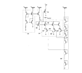
Referring now to Figure 3, a more detail
description of one embodiment of control circuitry 18
will be provided. In the embodiment of Figure 3,
control circuit 18 includes a conventional current
mirror 20, which supplies current to a diode-
connected transistor 22. Connected to the diode-
connected transistor 22 are a set of controllable
current paths 24. Each of these controllable current
paths is controlled by voltages supplied from a
voltage sensing circuit 26.
In Figure 3, current im/ from current mirror 20,
is caused to flow into diode-connected transistor 22.
This induces a voltage on line 16 which is applied to
the control gate of transistor 12 to control the
output current iout flowing through transistor 12.
The set of selectable of current paths 24, when
activated, draw current f rom current mirror 20 and
away from diode-connected transistor 22. This
reduces the voltage level on line 16, which in turn
reduces the control voltage applied to transistor 12,
and therefore reduces the output current iout.
Each of the current paths in the set of current
paths 24 is controlled by a voltage from the voltage
CA 02261733 1999-01-28
W O 98/0512~ PCTrUS97/12984
sensing circuit 26. More particularly, voltage
sensing circuit 26 is formed of a ladder of diode-
connected transistors. It is to be noted that each
o~ the controllable current paths 30 is connected to
a different node on the ladder, so that each of the
paths will be activated depending upon the magnitude
of the supply voltage applied at the top of the
ladder. For example, the controllable current path
controlled by the voltage at node 32 will be
activated when V9UPP1Y is 3 thresholds, VTI above
ground. In turn, the controllable current path 30
which is controlled from node 34 of voltage sensing
circuit 26 will be activated when VgUpply is 4
thresholds voltages above ground. It is to be
understood that by connecting the controllable
current paths to different points in the ladder of
voltage sensing circuit 26, the amount of current
drawn away from di.ode-connected transistor 22 can be
controlled as a function of the magnitude of supply
voltage V9upply~ It is further to be understood that
the threshold voltages of the diode-connected
transistors in the voltage sensing circuit 26 can be
made to be different (for example by varying the
physical size of the transistors) from the threshold
voltages of the transistors in controllable paths 30
so that further variations in control can be
obtained.
Turning now to the set 24 of controllable
current paths 30, each of the controllable current
paths 30 is preferably constructed of a pair of
series connected transistors, each pair of which is
connected in parallel with diode-connected transistor
CA 02261733 1999-01-28
WO98/05125 PCT~S97/129B4
22. One of the pair of transistors has its drain
connected to the drain of diode-connected transistor
22 and its gate connected to the gate of the diode-
connected transistor 22. The second transistor has
its drain connected to the source of the first
transistor, a source connected to ground, and a
control gate which receives a corresponding control
voltage from the voltage sensing circuit 26.
It is to be understood that the first transistor
36 c~n be sized to draw a predetermined amount of
current from current mirror 20 as a function of the
gate-source voltage induced across transistor 22.
For example, for a given gate-source voltage across
diode-connected transistor 22, transistor 36 can be
lS sized to draw l/l0 of the current flowing through
transistor 22 for the same gate-source voltage
supplied across diode-connected transistor 22.
Thus, it can be appreciated that under such
conditions if l0 controllable current paths are
provided in a set of controllable current paths 24,
the activation of all such paths will draw a
substantial amount of current from a current mirror
20 and away from diode-connected transistor 22, and
thereby cause the voltage VcOntrol at line 16, to be
reduced substantially. In turn, it can be seen that
as V~upply drops, fewer of the controllable current
paths will be activated, thereby increasing the
amount of current permitted to flow from current
mirror 20 into diode-connected transistor 22, thereby
raising the magnitude of the voltage at line 16, and
increasing the current flowing through transistor 12.
In this manner, a decreasing supply voltage causes an
CA 02261733 1999-01-28
W O 98/05125 PCTrUS97/12984
increase in the output current flowing through
transistor 12. Conversely, as V8upply increases, a
decreasing amount of current is permitted to flow
into diode-connected transistor 22, thereby causing a
decreasing magnitude of voltage being present at line
16. In turn, the magnitude of output current
provided by transistor 12 decreases with increasing
voltage supply.
Referring now to Figure 4, the circuitry
illustrated is similar to that in Figure 3, except
that a second set of controllable current paths 40,
and a second voltage sensing circuit 42, have been
added. The voltage sensing circuit 42 is constructed
similarly to voltage sensing circuit 26, but is
coupled to a reference voltage which can be supplied
by the user. Further, it is to be noted that the
control voltages are taken from different nodes of
the voltage sensing circuit 42 when compared to that
of sensing circuit 26. This means that a different
magnitude of voltage at Vref will be required to
activate different ones of the second set of
controllable current paths 40.
In light of Figures 3 and 4, it can be
appreciated that by the appropriate sizing of the
transistors and the controllable current paths 30,
and the selection of nodes in the voltage sensing
circuit 26 from which to derive control voltages, the
amount of current which is permitted flow into diode-
connected transistor 22 can be controlled as desired.
For example, the transistors in controllable current
paths 30 can be sized, and the control voltages from
voltage sensing circuit 26 selected, to provide an
CA 0226l733 l999-0l-28
W O 98/05125 PCT~US97/12984
output current which does not vary appreciable as the
supply voltage level varies. More particularly, the
controllable current paths would be controlled to
draw less current as the magnitude of the voltage
supply decreases, and the rate at which such decrease
occurs is selected to offset the rate at which
current mirror 20 decreases the magnitude of current
im with decreasing supply voltage. In this manner,
the current flowing through diode-connected
transistor 22 will remain substantially the same even
though the supply voltage is decreasing.
In situations where it is desired to have the
output current actually increase as the supply
voltage decreases, the transistor in the controllable
current paths 20 (and the control voltage points from
voltage sensing circuit 26) can be selected so that
the amount of current which is permitted to flow into
diode-connected transistor 22 is higher at low supply
voltages than it is at higher supply voltages.
~eferring to Figure 5, this latter condition is
illustrated by graph 44. Similarly, the situation in
which the current flow into diode-connected
transistor 22 is kept constant over the supply
variation, is illustrated in Figure 5 by graph 46.
Referring now to Figure 6, an embodiment of the
present invention is shown in which the output
current iout increases with increasing supply voltage.
The difference between Figures 3 and 4 versus Figure
6 is that in the controllable current paths of the
former, N-channel transistors are used for both 36
and 38. In contrast, in the embodiment in Figure 6,
an N-channel transistor is used for transistor 36,
CA 02261733 1999-01-28
WO98/05125 PCT~S97/12984
but a P-channel transistor 48 is used in place of the
N-channel transistor 38.
When V~upply is low, all controllable current paths
are on, but as the magnitude of V~upply increases, the
controllable current paths begin turning off. In
this fashion, the current which is permitted to flow
into diode-connected transistor 22 increases as the
supply voltage increases. The output current to
supply voltage relationship of Figure 6 is shown as
graph 50 in Figure 5.
It is to be understood that while certain
embodiments have been illustrated in the above
Figures, there are numerous other variations of the
present invention which can be constructed in the
spirit of the present invention. While the examples
describe have been given in terms of metal oxide
semiconductor transistors, bipolar and other devices
can be used.
The terms and expressions which have been
employed here are used as terms of description and
not of limitation, and there is no intention, in the
use of such terms and expressions, of excluding
e~uivalents of the features shown and described, or
portions thereof, it being recognized that various
modifications are possible within the scope of the
invention claimed.
--10-