Note: Descriptions are shown in the official language in which they were submitted.
CA 02261769 1999-O1-25
WO 98/OS807 PCT/LTS97/13527
CaTiOa INTERFACIAL TEMPLATE STRUCTURE ON SUPERCONDUCTOR
Background of the Invention
This invention relates generally to structures and
the preparation of such structures for use in semiconductor
and related applications and relates, more particularly, to
the growth of epitaxial thin films upon semiconductor-based
materials in the Group III-V, IV and II-VI classes such as,
by way of example and not limitation, silicon or silicon-
germanium alloys.
Electroceramic thin-films and, in particular,
ferroelectric oxides are known to support the phenomenon of
ferroelectricity and are believed to be useful in a wide range
of applications such as nonvolatile memories, optical
waveguides, and as a capacitor material in random access
memories (RAM), dynamic random access memories (DRAM),
electrically programmable read only memories (EPROM) and the
like. For example, in epitaxially grown ferroelectric oxide
layers wherein the crystallographic orientation of the layers
is ordered, the orientation of the ferroelectric dipole moment
is the basis for logic-state retention in nonvolatile
memories. Thus, it would be desirable to integrate a
ferroelectric oxide with a semiconductor-based substrate
comprised, for example, of silicon or silicon-germanium to
render a monolithic structure which possesses both
semiconductor and ferroelectric properties.
In solid state electrical devices of the prior art,
such as ferroelectric field effect transistors (FFETs) and
capacitors or inactive gate transistors which incorporate a
semiconductor material and a ferroelectric material, such as
a perovskite having the general formula ABO" the devices are
incapable of taking appreciable advantage of the ferroelectric
' and/or dielectric properties of the ferroelectric material.
For example, the FFETs constructed to date have been
- unsatisfactory in performance, and the capacitors and inactive
gate transistors constructed to date have been too leaky and
thus incapable of holding a charge for a lengthy period of
time. It would therefore be desirable to provide a solid
CA 02261769 1999-O1-25
WO 98/05807 PCT/US97/13527
2
state electrical device of this class which takes appreciable
advantage of the ferroelectric and/or dielectric properties
of the ferroelectric material incorporated therein.
Accordingly, it is an object of the present
invention to provide a new and improved structure comprised
of a crystalline electroceramic thin-film and a semiconductor
based substrate and a process for growing the thin-film upon
the substrate.
Another object of the present invention is to
provide such a structure which includes an ABO, material such
as, by way of example and not limitation, a perovskite, and
in particular a perovskite in the BaTiO, class, grown upon
materials selected from the Group III-V, IV or II-VI classes
of materials including, by way of example and not limitation,
a silicon or silicon-germanium substrate wherein the grown
perovskite is epitaxial and fully commensurate with the
underlying material upon which it is grown.
Still another object of the present invention is to
provide such a structure which utilizes a template structure
interposed between the material surface of the Group III-V,
IV or II-VI material forming the substrate and the desired
ABO, material such as a perovskite for facilitating the fully
commensurate growth of the desired ABO~ material upon the
substrate.
A further object of the present invention is to
provide a new and improved solid state electrical component
including a material adapted to exhibit ferroelectric,
piezoelectric, pyroelectric, electro-optic or large dielectric
properties during use of the component.
Summary of the Invention
This invention resides in a monolithic crystalline
structure and a process for growing an AB03 material, such as
a perovskite, film onto the surface of a Group III, IV or II-
VI semiconductor-based material wherein the material surface
provided is, by way of example and not limitation, a face-
centered-cubic (fcc) lattice structure like that of silicon
or silicon-germanium.
CA 02261769 1999-O1-25
WO 98/05807 PCT/US97/135Z7
3
The ABO, material has a lattice parameter which
matches the semiconductor surface cube on cube or which
closely approximates the quotient of the lattice parameter of
the semiconductor surface divided by the square root of 2.0
and further has a crystalline form comprised of two
constituent metal oxide planes comprised of AO and B02,
respectively. When the metal elements A and B of crystalline
form of the ABO, material are compared to one another, the
element A provides a large ration in the crystalline structure
of the ABO, material, and the element B provides a small
ration in the crystalline structure of the ABO, material.
For example, in an AB03 material wherein the element
B is the metal Titanium (Ti) (so that the B02 constituent
plane is TiO,), the Ti metal of the Tio2 plane provides a
small ration in the crystalline structure of the ABO,
material, and the metal oxide of the constituent metal oxide
plane AO includes the metal element A which provides the large
ration in the crystalline structure of the AB03 material. In
order to ensure commensurate periodicity during the buildup
of the A803 material, the formation of a single plane layer
consisting of a metal oxide (such as, for example, AO)
provided with a large ration is immediately followed by the
deposition of a single plane layer consisting of a constituent
metal oxide plane B02, rather than the constituent metal oxide
plane AO.
In addition, the ABO, material of the epitaxial film
is arranged upon the semiconductor surface so that a first
single plane consisting of the oxide constituent AO is fully
epitaxial and fully commensurate with the surface of the
substrate, and a second single plane consisting of the other
of the two constituent metal oxide planes (i.e. the oxide
plane of BO,) of the crystalline structure of the ABO,
material is fully commensurate with the first single plane of
AO and wherein the orientation of the AB03 material of the
film is matched either cube on cube with the lattice structure
of the substrate or is rotated 45° with respect to the
orientation of the material surface of the substrate.
CA 02261769 1999-O1-25
WO 98/05807 PCT/US97/13527 -
4
A process of the invention includes the steps of
providing a substrate of semiconductor-based material having
a surface which is provided by an fcc lattice structure like
that of silicon or silicon-germanium, and positioning the
substrate within an oxygen-free environment in an ultra-high
vacuum facility. Then, an alkaline earth oxide is selected
which has a lattice parameter which closely approximates the
lattice parameter of the material surface of the
semiconductor-based substrate, and then a film of the alkaline
earth oxide is grown upon the material surface wherein the
alkaline earth oxide film is at least one cell unit in
thickness. An ABO, material, such as a perovskite, is
subsequently selected which either has a lattice parameter
closely approximating the lattice parameter of the
semiconductor surface or the quotient of the lattice parameter
of the semiconductor surf ace divided by the square root of
2Ø The AB03 material has a crystalline form comprised of
two metal oxide planes wherein the metal oxide of one of the
two metal oxide planes is comprised of Bo2 so that the element
B of the BOZ plane provides a small cation in the crystalline
structure of the ABO, material and wherein the metal oxide of
the other of the two metal oxide planes includes another metal
which provides a large cation in the crystalline structure of
the ABO, material. A single plane of AO is grown upon the
alkaline earth oxide film wherein the AO of the single plane
is epitaxial and fully commensurate with the semiconductor
substrate, and then a single plane comprised of the other of
the two metal oxide planes ti.e. the oxide BOZ) of the
perovskite crystalline structure of the AB03 material is grown
upon the AO plane so that the metal oxide of the other of the
two metal oxide planes is epitaxial and fully commensurate
with the AO plane and wherein the orientation of the grown
ABO, material is either oriented cube on cube with respect to
the surface of the substrate or is rotated 45° with respect
to the surface of the substrate so that (001) perovskite is
parallel to (001) semiconductor surface and [100] perovskite
is parallel to [110] semiconductor surface.
CA 02261769 1999-O1-25
WO 98/05807 PCT/US97/13527 -
In one aspect of the invention, the structure is
formed by the process of the invention, and in another aspect
of the invention, the structure is in the form of a
ferroelectric field-effect (FFET) transistor including a base
5 substrate of silicon, a source electrode, a drain electrode,
a gate electrode, and a gate dielectric interposed between the
silicon and the gate electrode. In the FEET, the improvement
is characterized in that the gate dielectric includes an
epitaxial thin film layer of a perovskite oxide interposed
between the silicon and the remainder of the gate dielectric.
The construction process used to build up the FFET avoids any
tendency for undesirable silicon dioxide (Si02) to form at the
interface of the silicon and the gate dielectric.
Brig Desk intinn of t'he Drawing's
Fig. 1 is a perspective view of a silicon wafer upon
which a single crystal film of the perovskite BaTi03 can be
grown in accordance with the method of the present invention.
Fig. 2 is an exploded perspective view of a
structure within which a perovskite film is grown upon a
silicon substrate and illustrating schematically the
successive layers of constituents comprising the structure.
Fig. 3 is a schematic perspective view of a fragment
of the ultra high vacuum equipment with which steps of the
process of the present invention can be performed.
Fig. 4 is a plan view illustrating schematically the
orientation of the lattice structures of adjacent constituent
layers of the Fig. 2 structure.
Fig. 5 is a schematic cross sectional view of a
fragment of a ferroelectric field effect transistor (FFET)
utilizing a perovskite thin film as a gate dielectric.
Fig. 6 is a schematic cross sectional view of a
fragment of a capacitor utilizing a perovskite layer
juxtaposed with a layer of silicon.
Fig. 7 is a TEM photograph of a
BaTi03/CaTi03/Ba8r0/Si structure in accordance with an
embodiment of the structure of the present invention.
Fig. 8 is a graph wherein capacitance is plotted
CA 02261769 1999-O1-25
WO 98/05807 PCT/US97/13527 -
6
against gate voltage in tests performed upon an embodiment of
a structure in accordance of the present invention.
Fig. 9 is a graph wherein leakage current is plotted
against gate voltage in tests performed upon the structure
embodiment tested in Fig. 8.
Fig. 10 is a graph depicting the test results
involving a polarization-induced shift of the capacitance
voltage characteristics of an embodiment of a structure in
accordance with the present invention.
Detailed Descrig~ion of Illustrative Embodiments
The present invention truncates silicon with a
stable perovskite structure permitting growth of a thin-film
ferroelectric material on silicon as a monolithic structure.
It is a member of our general series of commensurate
structures designated as ( AO )"( A' BO ) m in which n and m are the
integer repeats of single plane commensurate oxide layers.
If n=1, then the perovskite is grown directly as AB03 from the
silicide truncation of silicon beginning at the AO plane. If
n>2, the face-centered NaCl-type structure is grown at the
interface then truncated with the B02 plane to transistion to
the perovskite structure.
With reference to Fig. 1, there is illustrated a
wafer or substrate 20 having a surface 22 upon which a single
crystal film of a material having the general formula ABO"
such as a perovskite (e.g. BaTi03), can be grown to produce a
monolithic structure embodying features of the structure of
the present invention. The substrate 20 is preferably of a
semiconductor-based material such as silicon or a silicon-
germanium alloy, but the substrate may be selected from group
consisting of Group IV, Group III-V and II-VI semiconductors.
The crystalline form of the AHO, material includes
a first single constituent oxide plane having the general
formula AO and a second constituent oxide plane having the
general formula BOz. While the element O of the formula ABOj
is understood to be oxygen, the element A may be a material
found in Group IA, IIA or IVB of the periodic table of the
elements, while the element B may be a material found in Group
CA 02261769 1999-O1-25
WO 98/05807 PCT/US97/13527 -
7
III, IVA or VA of the periodic table. When the metal elements
A and B of crystalline form of the ABO, material are compared
to one another, the element A provides a large cation in the
crystalline structure of the AB03 material, and the element B
provides a small cation in the crystalline structure of the
ABO3 material.
Briefly, during the build up of the desired AB03
upon the substrate surface 22, a first epitaxial and fully
commensurate film of an alkaline earth oxide (having the
general formula AO and a sodium chloride-type crystal lattice
structure) is grown upon the substrate surface 22, a second
f i lm ( of a desired A' B03 material ) is grown upon the first
film, and a third film (of the desired A'BO, material) is
grown upon the second film. The element A' of the A'BO,
material may, where AO is a single atomic layer, be the same
element A of the alkaline earth oxide AO having the sodium
chloride-type lattice structure but may, in other instances,
be an element other than the element A. Therefore, the
formula A'B03 appropriately is designated A'B03 to
differentiate, where in the case of a single atomic layer of
AO, the element A of the alkaline earth oxide AO is different
from the element A' of the constituent oxide A'O of the A'BOg
material. It will therefore be understood that in the
interests of the present invention, the element A' of the
formula A'BO, material can consist of, but is not limited to,
the element A of the alkaline earth oxide AO.
As the aforedescribed structure is grown, the
orientation of the crystalline form of the second film being
grown is either grown cube on cube or is rotated 45° with
respect to the orientation [e.g. (001) truncation] of the
first (alkaline earth oxide) film to facilitate the epitaxial
and fully commensurate build-up of the third film upon the
second film. Therefore and as will be apparent herein, the
first (alkaline earth oxide) film serves as a template upon
which the second film (of A'803 material) is grown, and the
second film serves as a template upon which the desired third
film (of A'HO, material) is grown.
CA 02261769 1999-O1-25
WO 98/05807 PCT/US97/13527 -
8
By way of example and not as limitation, the
specific monolithic structure described herein involves a
substrate 20 of semiconductor-based material comprised of
silicon, an alkaline earth oxide (AO) film comprised of
Bao.,2sSro.z,50. and an A'BO, material comprised of the perovskite
CaTiO, or, more specifically, perovskites of the CaTiO, class.
While the material of the substrate 20 is generally
characterized by a face-centered-cubic (fcc) lattice
structure, such as silicon and silicon-germanium alloys, the
alkaline earth oxide (AO) material includes a sodium chloride-
type lattice structure, and the perovskites of the CaTi03
class are generally characterized by a simple cubic lattice
structure. It will be understood, however, that the
principles of the present invention can be used to build up
thin-films of other A'B03 materials upon a substrate of
another semiconductor-based material, such as a silicon-
germanium alloy.
The techniques described herein to construct the
desired resultant monolithic structure are molecular beam
epitaxy (MBE) techniques. It will be understood, however,
that the described MBE techniques are intended for the purpose
of illustration and not as limitation. For example,
alternative methods, such as chemical vapor deposition (CVD)
and metal organic chemical vapor deposition (MOCVD), can be
employed. Accordingly, the principles of the present
invention can be variously applied.
As is described herein in accordance with an
embodiment of the method of the present invention and with
reference to Fig. 2, steps are taken to cover the surface 22
with a thin alkaline earth oxide film 24 of Bao_,25Sro_2,50, then
to cover the film 24 with a thin perovskite (template) film
26 of Cao.6,Sro.36Ti03, and then to cover the film 26 with a
desired (multi-stratum) perovskite film 28 of a perovskite of
the BaTi03 class to provide a resultant structure 32. Each of
the alkaline earth oxide film 24 and the template film 26 and
an appreciable portion of the perovskite film 28 are
constructed in somewhat of a single plane-layer-by-single
CA 02261769 2004-08-31
WO 98f05807 PCTlUS971I35Z7
9
plane-layer fashion, described herein, to ensure commensurate
periodicity throughout the build up of each film and wherein
the layer-construction processes take into account the
crystalline form of the material out of which the film is
desired to be constructed. Furthermore, the film-growing
processes described herein take advantage of the lattice
matching that exists at the interface of ad jacent films of the
structure 32. To this end, the lattice structures at the
interface of adjacent films have parameters which are matched
so that the likelihood of any appreciable lattice strain at
the fiim/film interface is significantly reduced. Moreover,
the growth process described herein avoids any propensity for
silica (SiO,) to form as an amorphous component of the
interface template structure.
Unlike the face-centered-cubic (fcc) crystalline
lattice structure of the semiconductor--based substrate 22, the
crystalline lattice form of perovskite is a simple cubic
structure and its crystalline (i.e. cube) form includes a
plane of a Group IVA element oxide, i.e. an oxide of a group
consisting of TiOZ, ZrO, and HfO~, and another plane of a
different metal oxide. For example and as discussed in U.S..
patent 5,450,812, having the sane inventors as the instant
application, the crystalline lattice structure of the
Similarly, the crystalline form of the perovskite SrTi.02
includes a plane of Ti02 and a plane of SrO.
perovskite BaTi03 includes a plane of Ti02 and a plane of BaO.
at the outset of a process performed in accordance
with the method of the present invention, the surface 22 of
the silicon substrate 20 is cleaned to atomic cleanliness so
that only silicon atoms are present at the surface 22. To
this end, the surface 22 is cleaned by a process common:iy
ref erred to as a Modi f fed RCS technique . The I~todi f i ed RCA
technique is a well-known process involving the chemical
production of an oxide at a silicon surface being cleaned and
subsequently placing the surface in a high vacuum environment
and raising the temperature of the surface to sublime the
CA 02261769 1999-O1-25
WO 98/05807 PCT/L1S97/13527 -
oxide off of the surface. (This same surface-cleaning
procedure is followed if the substrate 20 is comprised of a
silicon-germanium alloy.)
The layers of the desired structure 32 are built up
5 in this example by molecular beam epitaxy (MBE) , electron beam
evaporation techniques and with MBE equipment. The MBE
equipment includes an ultra high vacuum (UHV)
growth/characterization facility, a fragment of which is
indicated 40 in Fig. 3. The facility 40 includes a container
10 42 having an inner chamber within which the substrate 20 is
positioned so that its surface 22 faces downwardly, and a
plurality of canisters44, 46, 48 and 50 are provided within
the base of the container 42 for providing a vapor source of
metals desired to be added to the substrate surface 22 during
the formation of the structure 32. In this connection, each
canister 44, 46, 48 and 50 is adapted to hold a crucible
containing a desired metal and contains heating elements for
vaporizing the metal. An opening is provided in the top of
each canister, and a shutter is associated with the canister
opening for movement between a closed condition at which the
interior of the container is closed and thereby isolated from
the substrate surface 22 and an opened condition at which the
contents of the container , i . a . the metal vapors , are exposed
to the substrate surface 22.
In the depicted facility 4fl, an amount of the metal
barium (Ba) is positioned within the canister 44, an amount
of strontium (Sr) is positioned within the canister 46, an
amount of calcium (Ca) is positioned within the canister 48,
and an amount of titanium (Ti) is positioned within the
canister 50. In addition, an oxygen source 52 is connected
to the chamber so that by opening and closing a valve
associated with the source 52, oxygen can be delivered to or
shut off from the chamber. The opening and closing of each
canister shutter and the oxygen source valve is accurately
controlled by a computer controller (not shown).
Another feature of the facility 40 is that a
closable substrate shutter is disposed immediately below the
CA 02261769 1999-O1-25
WO 98/05807 PCT/US97/13527 -
11
downwardly-directed face of the substrate surface 22 for
isolating, when desired, the substrate surface 22 from
exposure to the metal vapors from the canisters or the oxygen
from the oxygen source 52 while the internal pressure of the
facility chamber is raised with the oxygen from the source 52.
The substrate shutter is closed during one step of the present
process as will be apparent herein.
The vacuum drawn in the UHV facility 40 to complete
the Modified RCA cleaning technique upon the substrate 20 is
l0 between about 10'9 and 10'1° torr, and the substrate 20 is
heated to raise the substrate temperature to a temperature
sufficient to drive the oxides off of the surface 22. In
practice, such a temperature may be between about 850 and
1050°C, and the desired surface cleanliness may be confirmed
in-situ during the substrate heating operation by Reflection
High Energy Electron Diffraction (RHEED) techniques. For
present purposes, the silicon substrate 20 reaches atomic
cleanliness upon the development of 2 x 1 Si(100) at the
surface 22 as evidenced by RHEED analysis.
Upon reaching the desired atomic cleanliness and to
initiate the growth of the first film 24 of the alkaline earth
oxide, a mixture of a predetermined amount of Barium (Ba)
metal and a predetermined amount of Strontium (Sr) metal is
deposited upon the substrate surface 22 so that a fraction,
e.g. about one-fourth, of a monolayer of the mixture covers
the substrate surf ace 2 2 . In other words , the Ba and Sr metal
mixture is deposited upon the substrate surface 22 until about
one atom of the mixture overlies the silicon surface 22 for
every four atomic sites of Si. To this end, Ba vapor and Sr
vapor is created in the corresponding canisters and the
corresponding canister shutters are opened to expose the clean
substrate surface 22 to the Ba and Sr mixture.
The ratio of Ba to Sr in the Ba/Sr vapor mixture is
selected with regard to the lattice parameter of the silicon
structure (or, in the alternative, the silicon-germanium
structure) of the substrate surface 22. In particular, the
lattice parameter of the silicon structure is known to be
CA 02261769 1999-O1-25
WO 98/05807 PCT/US97/13527 -
12
0.543 nm, and the lattice parameter of the structure of a
BaxSrl_x0 compound (formed upon the substrate surface 22 in a
manner described herein ) is selected to closely match that of
the silicon structure so that when epitaxialiy covering the
silicon surface 22, no appreciable strain exists at the
Si/BaxSrl_YO interface. In this connection, it is also known
that the lattice parameter of BaYSrI_x0 varies substantially
linearly as the ratio of Sr to Ba is increased in this
compound from 0.0~ to 100. Thus, when the variable "x" in
this compound equals 1.0, the lattice parameter of the
compound is 0 . 554 nm ( corresponding with the lattice parameter
of pure Ba0), and when the variable "x" in the compound equals
0.0, the lattice parameter of the compound equals 0.514 nm
(corresponding with the lattice parameter of pure Sr0).
In the depicted example, the ratio of Ba to Sr in
the BaYSrl_"O compound is selected to provide a lattice
parameter of the BaYSrl_x0 compound which exactly matches the
lattice parameter of silicon or, in other words, is selected
to provide the BaYSri_YO compound with a lattice parameter of
0.543 nm. To this end, the variable "x" in the this compound
equals 0.725 so that the proportion of Ba0 to Sr0 in the oxide
compound eventually formed upon the substrate surface 22 is
0.725 to 0.275.
In an alternative example in which the substrate 22
is comprised of silicon-germanium ( SiyGe1_,, ) , the ratio of Ba
to Sr in the BaxSr,,_Yc3 compound is selected to provide a
lattice parameter of the BaxSrl_RO compound which exactly
matches the lattice parameter of 5i,,Ge,_,,. If , for example,
the substrate 22 was comprised of Sio_goGeo_2o which has a
lattice parameter of 0.548 nm, the variable "x" in the
aforementioned BaxSr,_XO compound is selected to equal 0.85 so
that the proportion of Ba0 to Sr0 in the oxide compound
eventually formed upon the substrate surface 22 is 0.85 to
0.15 to provide the BaxSrl_x0 compound with a lattice parameter
of 0.548 nm.
For a more detailed description of the lattice
matching between adjacent films for the purpose of reducing
CA 02261769 2004-08-31
WO 98!05807 PCTIUS97I13527 -
13
lattice strain at a film/film interface of an epitaxial layup
of films, reference can be had to U.S. patent 5,482,003,
having the same inventors as the instant application.
Accordingly and with regard again to the exemplary
substrate 22 comprised of pure silicon, in the process step
described herein in which the Ba and Sr metals are deposited
upon a substrate of silicon so as to form a submonolayer
thereon involves the exposure of the substrate surface 22 to
a mixture of Ba and Sr vapors wherein the ratio of Ba to Sr
in the mixture is 0.725 to 0.275. Such exposure can be
effected with the facility 40 by either of two methods. One
method involves the production of a flux vapor of Ba and a
flux vapor of Sr from the canisters 44 and 46 containing Ba
and Sr, respectively, so that the combined vapor fluxes
emitted from the canisters provide the desired, i.e. target,
ratio of Ba to Sr in the Ha/Sr vapor mixture. The other
method involves the control of the amount of time that the
shutters of the Ba and Sr-containing canisters are opened so
that the appropriate amount of Ba and Sr vapors are emitted
from the corresponding canisters and become mixed in the
facility 40. In either event, the techniques used to produce
a mixture of metal vapors in the facility 40 wherein the vapor
mixture contains a desired ratio of one metal vapor to another
metal vapor involve techniques which are known and common to
IKBE so that the desired Ba to Sr in a mixture of Ba and Sr
vapors can be achieved in the facility with a high degree of
accuracy.
Upon completion of the deposition of the desired
fraction of the monolayer of Ba and Sr atoms upon the
substrate surface 22, the substrate 20 is cooled to between
about room temperature and 150'C while the high vacuum
environment is maintained about the substrate 20, and the
remainder of one monolayer of Ba and Sr is then deposited upon
the substrate surface. To this end, the shutters of the
canisters of Ha and Sr can be opened far an appropriate period
of time sufficient for the desired mixture of Ba and Sr vapor
CA 02261769 2004-08-31
WO 98/05807 PCT1US97/13527
14
(wherein the ratio of Ba to Sr in the vapor mixture is 0.725
to 0.275) is exposed to the substrate. By cooling the
substrate 20 to the lower temperature, i . a . between about room
temperature and 150°C, the attachment of Ba and Sr atoms to
the substrate surface is promoted because the added Ba and Sr
atoms remain in a metallic state and do not form silicide at
or below these lower temperatures.
As has been addressed in earlier U.S. patent
5.225,031, having the same inventors as the instant
application, the purpose for developing the monolayer of Ba
and Sr atoms at the Ha/Sz interface is to form a stable
template surface upon which a subsequent epitaxial layer of
Bao.",Sro."s0 is grown. Thus, with the stable monolayer of
Bao.",Sro,"60 formed upon the Si surface, Bao,,,sSro.=,s0 Can be
grown epitaxially upon the silicon in such a manner as to
avoid the fonaation of amorphous silica. To this end, the
substrate shutter is closed to prevent exposure of the
substrate surface 20 to the facility chamber contents, and the
pressure of the chamber is raised to about 1 to 5 x 10'' torr
of oxygen while maintaining Ba and Sr vapor source operations
that would be needed to deposit Ba and Sr metal upon the
substrate surface at a predetermined rate and in the desired,
or target, proportions of Ba to Sr. Upon reaching the target
oxygen pressure, e.g. 1 x l0'' torr, the substrate shutter is
opened to expose the 8a and Sr-coated surface of the substrate
to oxygen and additional Ha and Sr atoms. Upon such exposure,
Bao.",Sro_,.,~ begins to grow epitaxially upon the Ba and Sr-
coated surface.
By appropriately opening and closing off the
exposure of the substrate surface to the Ha and Sr metals and
oxygen by cyclically exposing the substrate surface to the Ba
and Sr metals and oxygen, Bao_"sSro_",O is grown upon the
substrate surface one atomic layer at a time. Such a growth
pattern is continued until the monolayers of Bao_",Sro.",0
develop sufficient stability to prevent the formation of an
amorphous silicate. It has been found that such stability is
CA 02261769 1999-O1-25
WO 98/05807 PCT/US97/13527
achieved upon the formation of a Bao-.,25Sro.Z,sO thickness of
about 1.0 nm (equivalent to about two cell units high), and
it is at this thickness of two cell units that the growth of
the film 24 is halted and the growth of the subsequent film
5 26 is initiated.
In other words, upon formation of the stable film
24 ( of two cell units in thickness ) of Bao.,2~Sro,"50 upon the
substrate surface 22, steps are taken to form the desired
template film 26 of Cao.6,Sro_36Ti03 upon the film 24. Whereas
10 the ratio of Ba to Sr in the film 24 of BaxSrl_x0 is selected
for its lattice match to that of the underlying silicon of the
surface 22, the ratio of Ca to Sr in the film 26 of CaxSrl_xTi03
is selected for its lattice match to that of the underlying
film 24 of Baa_,zSSro,2,so. However, whereas the film 24 is grown
15 epitaxially upon and is fully commensurate with the silicon
surface 22 so that its lattice orientation matches that of the
silicon surface 22, the crystalline form of the Cao.6,Sro.3gTiO3
film 26 (which is also epitaxial and fully commensurate with
the underlying film 24) has an orientation which is rotated
45° with respect to the orientation of the crystalline form
of the underlying Bao.,=sSro-=,g0 film 24. As will be apparent
herein, the build-up of the film 26 upon the film 24 effects
a change in the lattice structure of the construction from fcc
(i.e. of the underlying semiconductor-based material) to the
simple cubic lattice structure of a perovskite (i.e.
Cao.6,Sro.,6Ti03) while the perovskite build-up is fully
commensurate with the underlying semiconductor-based material,
and this build-up process is advantageous in this respect.
In this connection, CaTiO, and SrTi03 are mutually
soluble with one another and each has a cubic phase with a
continuously variable lattice parameter from 0.380 nm for
CaTi03 to 0.391 nm for SrTiO,. With this in mind, the
crystalline structure of the compound CaxSrl_YTi03 wherein
x=0.64 yields a lattice parameter of 0.384 nm, and this
lattice parameter matches, with a 45° rotation, the [110J
spacing of silicon (0.384 nm). Such a match of the
Cao.6,Sra.,6Ti0, lattice structure atop the Hao_~Zgsro,2~50 lattice
CA 02261769 1999-O1-25
WO 98/05807 PCT/US97/13527 -
16
structure is depicted in the plan view of Fig. 4 wherein the
Bao.,z~Sro.2,50 lattice structure (having a lattice parameter of
0.543 nm) is depicted in solid lines in Fig. 4 and the
Ca0.64Sr0-36T103 lattice structure ( having a lattice parameter of
0.384 nm) is depicted in phantom in Fig. 4. It follows that
the desired lattice parameter of the CaxSr,._%Ti03 crystal is the
quotient of the lattice parameter of the underlying
Baa.,z5Sro,2,50 crystal (0.543 nm) divided by the square root of
2.0 (i.e. approximately 1.414).
The above-discussed 45° rotation of the orientation
of the lattice structure grown atop another lattice structure
has been proven by growing a sample of CaxSr,_YTi03 on BaSrO/Si
in a growth sequence : TiOZ/CaSrO/Ti02/CaSrO/ . . . Ref lection
high energy electron diffraction (RHEED) from the (001)
surfaces of the initial Si compared with the ( 001 ) face of
CaTiO, show that epitaxy does develop with the expected 45°
rotation so that ( 001 ) CaTi03 is parallel to ( 001 ) silicon and
[100] CaTiO, is parallel to [110] silicon. The alloyed and
lattice matched CaYSrl_xTiO, thin films are stable after growth
as thin as 3 unit cells (less than 1.2 nm).
To grow the desired template perovskite film 26 of
Cao.6,SrQ.36Ti03 upon the f i lm 26 , steps are taken which
correspond to those set forth in the earlier-referenced U.S.
patent 5,450,812. Briefly and keeping in mind that the
crystalline form of the perovskite structure Cao.6,Sro.,6Ti0,
includes a plane of TiO, and a plane of Caa.6,Sro.360. single
planes of Tio= and Cao_g,Sro.~60 are grown in an alternating
fashion (starting with a single plane of TiOz) upon the
Bao.,~Sro.z"O film 24 until the desired thickness of the film
26 is obtained.
In preparation of the growth of an initial Ti02
plane of the film 26, the pressure in the UHV chamber is
adjusted to (or maintained) between about 2-5 x 10-' tort.
The desired plane of Ti02 is then built upon the Mg0 surface
by conventional MBE techniques while the internal pressure of
the facility 40 is maintained between about 2-5 x 10'' tort.
For example, Ti metal vapor could initially be deposited upon
CA 02261769 1999-O1-25
WO 98/05807 PCT/US97/13527 -
17
the Bao_,zSSro.z.,50 surface and then oxygen from the- source 40
could be released over the surface so that the desired layer
of Tio2 is formed at the Bao,,2sSro-2,5o surface. Alternatively,
the Bao,,25Sro.2,50 surface could be simultaneously exposed to Ti
vapor and oxygen, in controlled amounts, so that TiOz forms
and then accumulates on the Bao.,25Sro_2.,50 surface.
During either of the aforementioned deposition
processes involving the Ti02 layer, careful control of the MBE
operation is maintained to ensure that no more than a single
plane-layer, i.e. one plane, of Ti02 is deposited upon the
Bao.,25Sro.a,50 surface. The bulk form of the compound Ti02, as
characterized by the ordered surface structure formed in this
step, has a non-equilibrium structure and is not found in
nature, and there exists a tendency for the formed Ti02 to
accumulate into clusters if the Bao.,25Sro-250 surface is exposed
to a greater amount of Ti02 than is needed to comprise a
single plane of Ti02. Of course, if such clusters develop,
the TiO~ layer looses its order, and the ability to grow
ordered layers upon the Ti02 layer is destroyed. Thus,
careful control must be maintained over the deposition of Ti
vapor and the release of oxygen from the source 40 so that a
single plane, and only a single plane, of Tio2 accumulates at
ordered sites upon the Bao.,2sSra_2,50 surface ( i . a . directly
contacts and is fully commensurate with the Bao.,2$Sro.2,s0
surface.
Following the development of the desired initial
( single plane ) layer of TiOz upon the Bao-,2,Sro.z,50 surface, a
(single plane) layer of Cao.6,Sro.360 which comprises the other
plane of the perovskite Cao_6,Sro.,6Ti0, is grown upon the Tio2
layer. To this end, conventional MBE techniques are used to
grow the desired Cao.6,Sro-360 layer epitaxially upon and fully
commensurate with the formed Ti02 layer. For example, the
metal vapors Ca and Sr may be initially deposited upon the
Ti02 surface in the desired proportions, i.e. 0.64 to 0.36,
and then the oxygen may be subsequently released into the
chamber so that the Cao.6,Sro.360 forms upon the Ti02 surface.
Alternatively, the Ti02 layer could be simultaneously exposed
CA 02261769 1999-O1-25
WO 98105807 PCT/US97/13527
18
to Ca and Sr vapors and oxygen so that Cao.6,Sro.,60 accumulates
on the Tio2 layer. In either event, careful control should be
maintained over the deposition operation here so that one
plane, and no more than one plane, of the desired layer of
Cao.6,Sro_36O is developed at this stage upon the Ti02 layer.
Upon formation of the desired plane of Caa,6,Sro.,e0,
a second plane of Ti02 is grown upon the Cao.6,Sra.,60 plane in
accordance with the aforedescribed techniques used to grow
Ti02 onto the Bao.,2sSro.=,5o surface. Then, upon formation of
the desired second plane of Ti02, a second plane of Cao.6,Sro.,6O
is grown upon the second plane of Ti02.
Thereafter, single plane-layers of Ti02 and
Cao.6,Sro.,60 are formed in an alternating fashion until at least
about three cell units of the desired CaSrTiO, perovskite are
grown upon the Bao.,25Sro.~,s0 surface. It has been found that
the alloyed and latticed matched Cao_6,Sro.36Ti03 film is stable
after growth as thin as three unit cells ( 1. 2 nm) is obtained.
Accordingly, the growth of the film 26 is halted upon the
obtaining of a thickness of the film 26 of three unit cells.
Once the desired template film 26 of Cao.6.Sra.36Ti03
is formed, steps are taken to grow the desired perovskite film
28 upon the film 26. In the embodiment of the method
described herein and as mentioned earlier, the perovskite of
the film 28 is BaTiO" and steps can be taken to grow the
BaTi03 directly upon the film 26, but as will be discussed
herein, there exists alternative schemes by which a film of
BaTiO, is ultimately obtained.
To grow BaTi03 directly upon the template film 26,
steps are taken to grow BaTio, in a single plane-layer-by
single plane-layer, i.e. a constituent plane-by-constituent
plane, fashion until a critical cell unit height is achieved
or, in other words, until lattice strain ceases to appear at
the surface of the layup of planes. In this connection and
keeping in mind that the cubic crystalline form of BaTi03 is
comprised of a plane of Ti02 and a plane of the metal oxide
Bao, an initial film layer comprised of a single plane of Ti02
is grown epitaxially upon the surface of the Cao_6.Sro.36Ti03
CA 02261769 1999-O1-25
WO 98/05807 PCT/US97/13527 -
19
film 26. As discussed above in connection with the growth of
a Ti02 plane of the film 24 and while maintaining the internal
pressure of the facility 40 between about 2-5 x 10'' torr, Ti
metal vapor could initially be deposited upon the
Ca0,64~r0.36T1O9 surface and then oxygen from the source 40 could
be released over the surface so that the desired layer of Ti02
is formed thereon. Alternatively, the Cao,64Sro.36Ti03 surface
could be simultaneously exposed to Ti vapor and oxygen, in
controlled amounts, so that Tio2 forms and then accumulates on
the Cao.6,Sro.,6Ti03 surface. As has been described in
connection with the aforementioned deposition processes
involving a single plane-layer of Ti02, careful control of the
MBE operation is maintained to ensure that no more than one
plane of Ti02 is deposited directly upon the Cao-6,Sro_36Ti0,
surface.
Following the development of the desired layer of
TiOz upon the Cao.6,Sro_36Tio3 surface, a (single plane) layer of
Ba0 which comprises the other plane of the crystalline
structure of the perovskite BaTiO, is grown upon the initial
Ti02 plane. As is the case with the formation of the plane of
metal oxide Cao_6,Sro.,602 of the film 26, the metal oxide Ba0
can be grown directly upon the TiO~ plane by conventional MBE
techniques. For example, the metal vapor Ba may be initially
deposited upon the TiO, surface, and then the oxygen may be
subsequently released into the chamber so that the metal oxide
Ba0 forms upon the TiO~ surface. Alternatively, the TiOZ
layer could be simultaneously exposed to metal vapor and
oxygen so that the metal oxide Ba0 accumulates on the Ti02
layer. Again, careful control should be maintained over the
deposition operation here so that one plane, and no more than
one plane, of the desired metal oxide Ba0 is developed at this
stage upon the Tio~ layer and so that the pattern of metal
oxide deposited upon the TiOz layer is epitaxial and fully
commensurate with the TiOz of the TiOz layer.
Upon formation of the desired plane of metal oxide
Bao, another plane of Ti02 is grown upon the metal oxide plane
in accordance with the aforedescribed techniques used to grow
CA 02261769 1999-O1-25
WO 98/05807 PCT/US97/135~7 -
20 _
TiOz upon the Cao.64Sro_,6Ti03 surface of the film- 24. Upon
formation of the desired another plane of TiOz, another plane
of the metal oxide Ba0 is grown upon the second plane of Ti02.
Thereafter, single plane-layers of Ti02 and Ba0 are
formed in an alternating fashion until a critical thickness
of the desired perovskite BaTi03, corresponding in this
instance to a cell unit height of at least about twelve cell
units, is grown upon the film 24. In other words,
dislocations which may develop within the formed layers
nucleate so as to provide internal strain relief within about
the first twelve cell units so that lattice strain does not
appear at the surface of the layup of planes. Thus, the
surface defined by the twelfth cell unit is ordered and
substantially free of strain.
Once the strain-free surface of perovskite is
formed, steps can be taken to grow additional layers of the
peravskite 8aTi0, upon the build up of cell units. In this
connection, subsequent growth of the perovskite upon its
strain-free bulk form is homoepitaxial, rather than
heteroepitaxial so that the characteristics of the interface
between adjacent layers of Ti02 and the metal oxide Ba0 are
nat likely to present problems during growth. Thus, the
perovskite can be built upon itself in layers which are each
one cell unit in height after the initial twelve cell units
of the perovskite are formed. To this end, the perovskite
BaTiO, is grown single cell-layer-by-single cell-layer upon
the strain-free surface by conventional MBE techniques so that
each layer grown during this stage is one cell unit high. For
example, the strain-free surface of perovskite may initially
be exposed to Ti and the metal Ba vapors and then to oxygen
so that the perovskite forms upon the strain-free surface.
Alternatively, the strain-free surface can be exposed
simultaneously to the Ti and Ba vapors and oxygen so that the
perovskite forms and then settles upon the strain-free
surface. Still further, known co-deposition techniques (e.g.
other than MBE processes) can be employed to grow the
perovskite in this stage of the growth process. In either
CA 02261769 1999-O1-25
WO 98/05807 PCT/US97/13527 -
21
instance, careful control of the build up process is
maintained so that the build up of successive layers of the
perovskite is effected epitaxially.
As an alternative to growing BaTiO, directly upon
the film 26 of Cao.6,Sro.36Ti0" an intermediate perovskite film
of BaxSrl_xTiO, can be grown upon the film 26, wherein the
variable "x" in the composition is chosen so that the lattice
parameter of the perovskite crystalline structure is closer
to that, i . a . 0 . 384 nm, of the underlying Cao.6,Sro-,6Ti0,
perovskite film than is the lattice parameter of BaTiO, (which
is 0.4 nm) . To this end, the variable "x" in the BaYSr,_xTiO,
compound is chosen to be 0.725.
To grow Bao-,zSSro-z~5TiO, upon the film 26 and keeping
in mind that the crystalline structure of this perovskite
includes a single plane of TiOZ and a single plane of
Hao.,~5Sro_"SO, an initial film layer comprising a single plane
of Ti02 is grown epitaxially upon the surface of the
Cao.6.Sro.36Ti0, film 26. The aforedescribed conventional MBE
techniques can be used to grow the initial film layer of TiOZ.
Of course and has been described in connection with the build
up of the Cao.6,Sro-,6Ti0, and BaTiO, films, careful control of
the MBE operation is maintained during the build up of this
initial single plane-layer of Ti02 to ensure that one plane,
and no more than one plane, of TiOz is grown upon the
Cao.6,Sro_,6Ti03 surface.
Subsequent to the build up of the initial Ti02
plane, Bao.,zsSro_"50 which comprises the other plane of the
perovskite Bao_,2sSro."~TiO, is formed upon the single plane
layer of Ti02. To this end, conventional MBE techniques are
used to grow the desired Bao.~zsSro.Z,50 layer upon the formed
TiOs layer. For example, the metal vapors Ba and Sr may be
initially deposited upon the TiOz surface in the appropriate
ratio 0.725 to 0.275, and then the oxygen may be subsequently
released into the chamber so that the desired Bao.,2sSra."~O
forms upon the Ti02 surface. Alternatively, the Ti.02 layer
could be simultaneously exposed to Ba and Sr vapors in the
appropriate amounts and oxygen so that the desired Bao-"sSro-Z,50
CA 02261769 1999-O1-25
WO 98/05807 PCT/US97/13527 -
22
accumulates on the Ti02 layer. Again, careful control should
be maintained over the deposition operation here so that no
more than one plane of the desired layer of Bao..,25Sro.2,5~ is
developed at this stage upon the Ti02 layer and so that the
pattern of Bao_,25Sro.z,go deposited upon the Ti02 layer is
epitaxial and fully commensurate with the Ti02 of the
previously-grown initial Ti02 plane.
Upon formation of the desired plane of Baa..,~Sro-Z,~O,
a further plane of Ti02 is grown upon the Bao..,258ro.2,s~ plane in
accordance with the aforedescribed techniques used to grow
TiO~ onto the Bao_~25Sro.Z,S~ surface. Then, upon formation of
the desired further plane of Ti02, a further plane of
Bao-,2sSro.2,so is grown upon the further plane of TiOz.
Thereafter, single plane layers of Ti02 and Bao.,a5Sra.2,5o are
grown in an alternating fashion atop one another until a cell
height is reached at which no lattice strain appears in the
last-grown layer, or plane, of Bao.,ZSSro.2~5~ ~ In other words,
any lattice strain which may exist at the
Bao..,~5Sro.2,50/Cao.6.Sro.,6Ti0~ interface is not as apparent as the
surface of subsequently-formed layers of Ti02 and Baa."sSro.~s0.
Along these lines, it is believed that no such strain will
appear following a build up of about four cell units of the
Bao.,~5Sro.z,5Ti0, perovskite structure upon the Cao.6,Sro_,6Ti0, film
26.
Following the growth of the Bao.,2,Sro_"9Ti0,
perovskite structure, BaTiO, can be grown upon the
Bao.,25Sro.~.,~Ti03 surface one cell unit layer-at-a-time by
conventional MBE techniques so that each layer constructed at
a stage of the build up process is one cell unit high. For
example, the Bao_,25Sro.z~5Tio3 surface may be initially be
exposed to Ti and Ba vapors and then to oxygen so that BaTiO,
perovskite forms upon the strain-free surface. Alternatively,
the Bao,,~Sra.2,5Ti03 surface can be exposed simultaneously to
the Ti and Ba vapors and oxygen so that the BaTi03 perovskite
forms and then settles upon the Bao-,zsSro,Z,sTi03 surface. In
either instance, careful control of the MBE process is
maintained so that the build up of successive layers of the
CA 02261769 1999-O1-25
WO 98/05807 PCT/US97/135Z7 -
23
perovskite is effected epitaxially. The growth of BaTiO, is
continued until the desired thickness of BaTiO, is obtained.
To illustrate the ordered arrangement of a multi
plane structure embodying the desirable features which can be
achieved with the process described above, there is shown in
Fig . 7 a transmission electron micrograph ( TEM ) of a cross
section of a BaTiO,/CaTiO,/BaSrO/Si structure in accordance
with an embodiment of the structure of the present invention.
The layer of BaSrO which directly contacts and is fully
commensurate with the underlying substrate of silicon is four
atoms thick, and the BaSrO interface with silicon is
atomically sharp with no evidence that amorphous silica is
present at that interface. By comparison, the layer of CaTiO,
which directly contacts and is fully commensurate with the
underlying layer of BaSrO is eight atoms thick. A layer of
the perovskite BaTiO, directly contacts and is fully
commensurate with the underlying layer of CaTiO,. It can be
seen within this Fig. 7 TEM that the atoms of the various
layers are highly ordered and uniform and that the planes
comprising the various layers of the Fig. 7 structure are
substantially defect-free.
It will be understood that although the
aforedescribed structure has been described as involving a
build up of BaTiO, upon a semiconductor-based substrate, other
perovskites can be constructed in accordance with the broader
aspects of the invention. Such perovskites include those in
the BaTiO, class such as GaTiO" PbTiO" PbLaTiO" Pb(Zr Ti)O"
( PbLa ) ( ZrTi ) O" SrTiO" KNbO" KTaO" NaNbO" NaTaO" LiNbO"
LiTaO" CaTiO" LaAlO" NaTaO, and YBCO.
Although the build up of the structure 32 has been
described as involving the use of an intermediate template
layer 26 of CaxSrl_%TiO, wherein x=0.64, we have found
experimentially (i.e. verified through RHEED analysis) that
in order to achieve the desired commensurate periodicity
between sequentially-built single-plane layers, the ratio of
Ca to Sr within the single plane layers of CaxSrl_YO may fall
within a relatively broad range (e. g. wherein "x" may fall
CA 02261769 1999-O1-25
WO 98/05807 PCT/US97/13527 -
24
within the range of between 0.5 and 0.8). Accordingly,
wherein "x" is described within the layer 26 Of CaxSr,,_xTi03 in
the aforedescribed structure as equal to 0.64, the value of
"x" is not necessarily so limited.
~erroe~ectric Considerations
It is recognized in the art that ferroeiectric
materials , such as perovskites , can be advantageously used in
solid state electrical components if incorporated therein in
a manner which takes appreciable advantage of the
ferroelectric and/or dielectric properties of the materials.
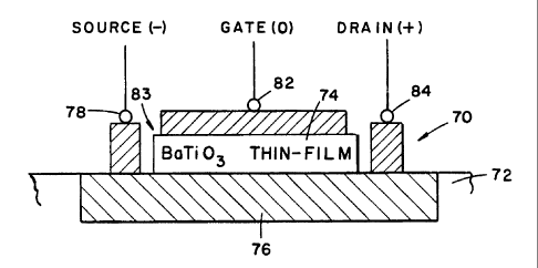
For example and with reference to Fig. 5, there is shown a
ferroelectric field effect transistor (FFET), indicated 70,
including a base, or substrate 72 of Si and an overlayer 84
of the perovskite BaTi03. The transistor 70 is also provided
with a source electrode 78, a drain electrode 80, a gate
electrode 82, and a gate dielectric 83. The BaTi03 thin-film
84 (which comprises a portion of the gate dielectric 83) is
sandwiched between the epilayer 76 and the remainder of the
gate dielectric 83 so as to be positioned adjacent the
epilayer 76. Since ferroelectric materials possess a
permanent spontaneous electric polarization (electric dipole
moment per cubic centimeter) that can be reversed by an
electric field, the ferroelectric dipoles can be switched, or
flipped, and the charge density and channel current can be
modulated. Thus, the transistor 70 can be turned ON or OFF
by the action of the ferroelectric polarization, and if used
as a memory device, the transistor 70 can be used to read the
stored information (+ or -, or "1" or "0") without ever
switching or resetting (hence no fatigue).
Similarly, there is schematically depicted in Fig.
6 a capacitor 90 for a dynamic random access memory (DRAM)
circuit including a silicon layer 92 and an oxide (dielectric)
layer 94 which are in superposed relationship and which are
sandwiched between a gate 96 and a ground terminal 98. In
use, an information-providing signal is collected from the
capacitor 90 by measuring the current of the capacitor 90
during a discharge cycle. Therefore, the greater the
CA 02261769 1999-O1-25
WO 98/05807 PCT/US97/13527
dielectric constant exhibited by the oxide layer 94, the
greater the charge-storage capacity of the capacitor 90.
Since ferroelectric materials, such as perovskites, are known
to be capable of exhibiting relative large dielectric
5 constants (e. g. at least 1000), a perovskite-including
capacitor which takes appreciable advantage of the desirable
dielectric properties of the perovskite would be advantageous.
Heretofore, however, in the case of each of the
ferroelectric field effect transistors and capacitors or
10 inactive gate transistors which incorporate a ferroelectric
material, such as a perovskite, the devices are incapable of
taking appreciable advantage of the ferroelectric and/or
dielectric properties of the ferroelectric materials. The
FFETs constructed to date have been unsatisfactory in
15 performance, and the capacitors and inactive gate transistors
constructed to date have been too leaky and thus incapable of
holding a charge for a lengthy period of time. Factors which
are responsible for the unsatisfactory performance of FFETs
or ferroelectric material-including capacitors or inactive
20 gate transistors include the impurities (e. g, amorphous
nature) of the crystalline structure of the material or the
interface between the ferroelectric material and the
underlying silicon which interferes with the flow of current
within the device. For example, some interf ace materials
25 employed in FFETs can screen and thereby trap charge that
could otherwise contribute to the depleted or accumulated
state of the current-carrying channel of the device.
The aforedescribed process of the present invention
can be used to incorporate a ferroelectric material, i.e. a
perovskite, in a solid state electrical component, such as a
FFET and a capacitor for a RAM or DRAM circuit, during the
construction of the component which enables the component to
take appreciable advantage of the ferroelectric and/or
dielectric properties of the ferroelectric material during
use. In other words, by building up a desired perovskite
directly upon silicon with the use of the template structure
as described above, the crystalline quality of the resulting
CA 02261769 1999-O1-25
WO 98/05807 PCT/US97/13527 -°
26
perovskite is high, and the interface between the-perovskite
and the silicon is stable. Along these lines, the few layers
of non-perovskite interface material which provide the
template structure upon which the perovskite is constructed
are commensurate with less than 1.0 x 10° site fraction errors
thereby achieving a monolithic interface structure. Thus,
interface trap densities of less than 1011 per square cm are
achieved.
When applying the foregoing to FFET construction and
with reference again to Fig. 5, the overlayer 84 of the
perovskite BaTi03 is grown upon the substrate 72 of Si in
accordance with the process of the present invention to
provide the FFET 70 with an overlayer 72 of high crystalline
quality and with a stable perovskite/silicon interface.
Similarly, when applying the foregoing to capacitor
construction and with reference again to Fig. 6, the oxide
layer 94 of the capacitor 90 can be provided by the perovskite
BaTio3 grown upon the silicon layer 92 in accordance with the
process of the present invention to provide the capacitor with
an oxide layer 94 of high crystalline quality and a stable
oxide/silicon interface structure. This construction, when
suitably modified as previously noted, is also applicable to
silicon-germanium-based devices.
Moreover, by exactly matching the lattice parameters
of an overgrowing oxide with those of silicon, heteroepitaxy
with a perovskite structure like BaTiO, can be accomplished
avoiding interfacial strain and thereby improving the
interfacial coherence and crystalline quality of the
silicon/ferroelectric thin-film structure. Furthermore, the
long range structural coherence of single crystal BaTiO, thin
films on silicon improve the dielectric properties of thin
film memory devices and significantly improve their fatigue
life in read-write-restore cycles of a conventional memory
circuit which is normally limited by the formation and
interaction of both line and planar defects in polycrystalline
materials presently used. Still further, the absence of
internal grain boundaries, strain, and electrostatic field
CA 02261769 1999-O1-25
WO 98/05807 PCT/US97/13527
27
effects commonly associated with the grain boun&aries will
significantly extend the useful life of a thin film
ferroelectric memory structure.
To substantiate that an embodiment of a structure
of the present invention does indeed possess the desirable
qualities addressed above, there is provided in Figs. 8-10
graphs of data collected from samples comprised of a layer of
BaTi03 constructed atop a silicon substrate in accordance with
an embodiment of the method of the present invention. In
particular, Fig. 8 is a graph depicting the measured
capacitance versus gate voltage of a layer of BaTi03 ( 0 . 280 nm
in thickness) constructed upon silicon. The curve drawn
through the plotted points characterize that of a substance
suitable for use as a capacitor (e. g. an MOS capacitor).
Along the same lines, the Fig. 9 plot which shows the leakage
current versus gate voltage of the material illustrates a low
leakage current (i.e. less than 10'' amps per square
centimeters at 3.0 volts) - a quality indicting that the
material (as a capacitor) will hold a charge for an
appreciable period of time. Furthermore, the curves depicted
in Fig. 10 evidence a threshold voltage shift (of about 1.0
volt) as a consequence of a polarization reversal in the
ferroelectric gate oxide. Therefore, when the structure is
used in conjunction with a FFET (such as the FFET 70 of Fig.
5), the polarization reversal switches the silicon and thus
switches the device ON or OFF.
Still further, a sample capacitor construction
(constructed in accordance with the method of the present
invention) including a thin-film of BaTiO, (of 0.280 nm in
thickness) grown onto an interface thin-film of CaTiO, (of
0.40 nm in thickness) grown onto a silicon substrate has been
found to possess the following MOS capacitor characteristics:
The flat band voltage measured -1.027 volts; the threshold
voltage measured -0.29 volts: the Al/Si workfunction (volts)
measured -0 . 95 volts : the interf ace charge ( coul/cm' ) measured
6 . 04 x 10-8 coui/cm2: and the trap density ( 1/cm=) measured
3.77 x 10¹¹. In addition, the resistivity-voltage, ,has been
CA 02261769 1999-O1-25
WO 98/05807 PCT/LTS97/13527
2a
found to be 101'ohm-cm, and the leakage current is-less than
1 x 10'9 amps/cm' at 3 volts. The foregoing measurements were
made with aluminum electrodes, 160 dam pads, p-doped 10'6/cm~.
It follows from the foregoing that a FFET and a
process for constructing the FFET has been described which
improves upon conventional FET structure. In particular, a
monolithic structure and grocess has been described which
accommodates the lattice mismatch between silicon and a
perovskite, such as BaTiO" if a single crystal of the
perovskite is to be grown upon silicon. After limiting the
thickness of the initially-grown alkaline earth oxide film to
two unit cells (e.g. 2 x 0.543 nm, or 1.068 nm) , a unique
transition is made to a perovskite structure, CaTio, (having
a cubic lattice parameter of 0.380 nm) which can be alloyed
with Sr to exactly lattice match silicon. Since CaTi03 and
SrTiO, are mutually soluble in each other and have a cubic
phase with continuously variable lattice parameter from 0.380
nm far CaTi03 to 0.391 nm for SrTi03, the composition Ca,~Sr,_
xTi03 wherein x=0.64 has a crystalline structure which, with
a 45° rotation of its orientation, lattice-matches the [110]
spacing of silicon (0.384 nm). BaTiO, or SrTiO, are simple
cubic perovskites and when grown epitaxially upon CaYSr,_xTiO,
on BaSrO/Si as the active component in a composite
ferroelectric structure developed on silicon, are the central
elements of a thin film memory circuit.
Similarly, it follows from the foregoing that a
ferroelectric material-including capacitor or an inactive gate
transistor and a process for constructing the device has been
described which improves upon conventional capacitor or
inactive gate transistor. Whereas in a FFET, the
ferroelectric material incorporated therein is used fn a
ferroelectric state as a ferro-gated transistor, in
applications such as a capacitor used in a DRAM circuit or an
inactive gate transistor, the ferroelectric material is used
in a non-ferroelectric state, but as a high dielectric
constant configuration for inactive gate transistors or
capacitors.
CA 02261769 1999-O1-25
WO 98/05807 PCT/ETS97/I3527 -
29
It will be understood that numerous modifications
and substitutions can be had to the aforedescribed embodiments
without departing from the present invention. For example,
while much of the foregoing discussion has focused upon the
ferroelectric qualities of a perovskite constructed on a
semiconductor-based material, it will be understood by one
skilled in the art that many comparable devices can be
constructed in accordance with the principles of this
invention which possess other desirable characteristics. For
example, comparable devices can be constructed which are
piezoelectric in nature, pyroelectric in nature or electro-
optic in nature. Accordingly, the aforedescribed embodiments
are intended for the purpose of illustration and not as
limitation.