Note: Descriptions are shown in the official language in which they were submitted.
CA 02261826 1999-02-15
DIGITAL MODULATION SYSTEM USING MODIFIED ORTHOGONAL
CODES TO REDUCE AUTOCORRELATION
BACKGROUND OF THE INVENTION
1. Field of The Invention
This invention relates to wireless communication systems and, more
particularly, to a digital modulation system that uses modified orthogonal
codes, such
as M-ary orthogonal Keying (MOK) to encode information.
2. Description of Related Art
1 o A wireless communications channel can rarely be modeled as purely line-of
site.
Therefore, one must consider the many independent paths that are the result of
scattering
and reflection of a signal between the many objects that lie between and
around the
transmitting station and the receiving station. The scattering and reflection
of the signal
creates many different "copies" of the transmitted signal ("multipath
signals") arriving at
the receiving station with various amounts of delay, phase shift and
attenuation. As a
result, the received signal is made up of the sum of many signals, each
traveling over a
separate path. Since these path lengths are not equal, the information carried
over the
radio link will experience a spread in delay as it travels between the
transmitting station
and the receiving station. The amount of time dispersion between the earliest
received
2o copy of the transmitted signal and the latest arriving copy having a signal
strength above
a certain level is often referred to as delay spread. Delay spread can cause
intersymbol
interference (ISI). In addition to delay spread, the same multipath
environment causes
severe local variations in the received signal strength as the multipath
signals are added
constructively and destructively at the receiving antenna. A multipath
component is the
combination of multipath signals arnving at the receiver at nearly the same
delay. These
variations in the amplitude of the multipath components is generally referred
to as
Rayleigh fading, which can cause large blocks of information to be lost.
Digital modulation techniques can be used to improve the wireless
communication link by providing greater noise immunity and robustness. In
certain
3o systems, the data to be transmitted over the wireless communication link
can be
CA 02261826 1999-02-15
2
represented or encoded as a time sequence of symbols, where each symbol has M
finite
states, and each symbol represents N bits of information. Digital modulation
involves
choosing a particular code symbol from the M finite code symbols based on the
N bits
of information applied to the modulator. For M-ary keying schemes, log2M bits
of
information can be represented or encoded by M different codes or code symbols
which
are transmitted. The transmitted codes are received as several delayed
replicas of the
transmitted codes, and the receiver correlates the delayed versions of the
received
codes with the known codes by performing a summation of autocorrelation values
for
all possible multipath delays.
1 o The autocorrelation sidelobes show the correlation values between the
known
codes and the time shifted replicas of the received codes. If a code is the
same or is a
shifted version of itself, then the code will have a high level of
autocorrelation or
autocorrelation sidelobes. For example, for a code ( 111-1 ), the
autocorrelation for a
zero shift is:
t 5 code 1 1 1 -1
shifted code 1 1 1 -1
multiplication 111 1
correlation = sum of multiplied values = 4.
For a shift of one chip, the autocorrelation is:
2o code 1 1 1 -1
shifted code 1 1 1 -1
multiplication 1 1 -1
correlation = sum of multiplied values = 1.
For a shift of 2 chips, the autocorrelation is:
25 code 1 1 1 -1
shifted code 1 1 1 -1
multiplication 1 -1
correlation = sum of multiplied values = 0.
For a shift of 3 chips, the autocorrelation is:
3o code 1 1 1 -1
CA 02261826 1999-02-15
3
shifted code 1 1 1 -1
multiplication -1
correlation = sum of multiplied values = -1.
Larger shifts give an autocorrelation value of zero, so the maximum
autocorrelation
sidelobe in this example has a value or magnitude of 1. In this example, -1's
are used
in the receiver instead of 0's. The autocorrelation sidelobes give an
indication about
multipath performance. If the autocorrelation sidelobes are large, several
multipath
components heavily interfere with each other.
Cross-correlation refers to a code being correlated with different codes. M-
1 o ary orthogonal keying is a form of digital modulation which provides good
cross-
correlation between codes by encoding data using orthogonal codes which do not
interfere with each other. FIG. 1 shows a general block diagram of an M-ary
orthogonal keying system 10. In this example, input data is scrambled by a
scrambler
12 as specified in the current Institute of Electrical and Electronics
Engineers (IEEE)
802.11 standard. The data is then provided to a serial-to-parallel converter
14 which
converts the serial data into 8 parallel bits forming a data symbol. A first
modulator
16 receives three (3) of the parallel bits and produces a code of length 8
chips from a
look-up table, and a second modulator 18 receives three (3) of the parallel
bits and
produces a second code of length 8 from a look-up table. Chips are actually
code bits,
2o but they are called chips to distinguish them from data bits. In this
implementation,
one of the parallel bits is provided to a first exclusive-or (XOR) gate 20
which inverts
the code if the bit has a value of one. Similarly, the last remaining bit is
provided to a
second XOR gate 22 which inverts the code from the second modulator 18 if the
bit has
a value of one. In this embodiment, the output Io"t of the XOR gate 20 is
applied to
signal circuitry 21 to convert all 0's to -1's for transmission. The circuitry
21 can also
manipulate, convert and/or process Io"t before being used to modulate a
carrier with
frequency ~ by mixer 24. The output Qo"L from the XOR 22 is applied to signal
circuitry 23 to convert all 0's into -1's for transmission. The circuitry 23
can
manipulate, convert and/or process Qo,~ before being used to modulate a 90
degrees
3o shifted carrier by mixer 26. In this particular embodiment, the first
modulator 16
CA 02261826 1999-02-15
4
corresponds to the in-phase (I) component of the output signal, and the second
modulator 18 corresponds to the quadrature (Q) component of the output signal.
The modulators 12 and 14 are performing M-ary orthogonal keying or
encoding because each receive log2M bits of information and chooses one out of
M
orthogonal codes. By having both I and Q components with different polarities,
a
total of (2M)2 possible code combinations exist, so a total of 2+21og2M bits
can be
encoded into one orthogonal code. In this example, M is equal to 8. The M
codes in
an M-ary orthogonal keying system are usually based on M chip Walsh codes.
Using
the M chip Walsh codes in an M-ary orthogonal keying system is advantageous
1 o because the M chip Walsh codes are orthogonal, which means they exhibit
zero cross-
correlation, so the M chip Walsh codes tend to be easily distinguishable from
each
other. However, using Walsh codes as the orthogonal codes can create potential
problems. For example, when Walsh code 0 (all 1's) is selected as the code
symbol,
Walsh code 0 may appear as an unmodulated continuous wave (CW) carrier signal.
To avoid the Walsh code 0 CW modulation, M-ary orthogonal keying systems
have been proposed which use a cover sequence of ( 11111100) to modify the
Walsh
codes by inverting the last two bits of each Walsh code. Although the Walsh
code 0
CW modulation is resolved by modifying the Walsh codes in this fashion, the
modified Walsh codes retain the poor autocorrelation and spectral properties
which
2o are inherent to Walsh codes. To counter the poor autocorrelation and
spectral
properties of the Walsh codes, current systems multiply the output signal by a
pseudo-random noise (PN) sequence. Some systems multiply by a PN sequence
having a length much larger than the Walsh code as described in E. G.
Tiedemann,
A.B. Salmasi and K.S. Gilhousen, "The Design And Development of a Code
Division
Multiple Access (CDMA) System for Cellular and Personal Communications,"
Proceedings of IEEE PIMRC, London, September 23-25, 1991, pp.131-136. Other
systems multiply the Walsh codes by a PN sequence with the same length as the
Walsh code. However, the autocorrelation properties of the resulting codes are
still
lacking. If the transmitted codes lack sufficient autocorrelation properties,
the
CA 02261826 1999-02-15
multipath performance of the system can be poor because the system will have
di~culty detecting the delayed or shifted versions of the transmitted codes.
SUMMARY OF THE INVENTION
5 The present invention involves a digital (de)modulation system which
provides enhanced multipath performance by using modified orthogonal codes
with
reduced autocorrelation sidelobes while maintaining the cross-correlation
properties
of the modified codes. The modified orthogonal codes have autocorrelation
sidelobes
that do not exceed one-half the length of the modified orthogonal code. In
certain
1 o embodiments, an M-ary orthogonal keying (MOK) system is used which
modifies
orthogonal Walsh codes using a complementary code to improve the auto-
correlation
properties of the Walsh codes, thereby enhancing the multipath performance of
the
MOK system while maintaining the orthogonality and low cross-correlation
characteristics of the Walsh codes.
BRIEF DESCRIPTION OF THE DRAWINGS
Other aspects and advantages of the present invention may become apparent
upon reading the following detailed description and upon reference to the
drawings in
which:
2o FIG. 1 shows a block diagram of a M-ary orthogonal keying {MOK) system
using Walsh codes modified by a cover sequence ( 11111100);
FIG. 2 shows a block diagram of a digital modulation system using modified
orthogonal codes to reduce the autocorrelation sidelobes of the orthogonal
codes;
FIG. 3 shows a block diagram of an embodiment of a MOK system according
to the principles of the present invention;
FIG. 4 shows a graphical comparison of packet error ratio versus delay spread
for a MOK system using Walsh codes modified by a cover sequence in current
systems v. modified Walsh codes to reduce the autocorrelation sidelobes;
FIG. 5 shows a block diagram of another embodiment of the MOK system
3o according to the principles of the present invention;
CA 02261826 1999-02-15
6
FIG. 6 shows a graphical comparison of packet error ratio versus delay spread
for embodiments of the MOK system using Walsh codes modified by a cover
sequence in current systems v. modified Walsh codes to reduce the
autocorrelation
sidelobes;
FIG. 7 shows a block diagram of another embodiment of the MOK system
according to certain principles of the present invention;
FIG. 8 shows a digital demodulator according to certain principles of the
present invention;
FIG. 9 shows a demodulation system using the digital demodulator according
to certain principles of the present invention; and
FIG. 10 shows another embodiment of a demodulation system using the
digital demodulator according to the principles of the present invention.
DETAILED DESCRIPTION
t 5 Illustrative embodiments of the digital (de)modulation system to enhance
multipath performance for a wireless communications system is described below.
FIG. 2 shows a digital modulator 28 according to the principles of the present
invention. In response to data bits, the modulator 28 chooses a corresponding
one of
M codes. The M codes are produced by modifying a set of orthogonal codes to
2o reduce the autocorrelation levels associated with those orthogonal codes
while
maintaining the orthogonality of the set. For example, if the same chips) in
the
codes of the orthogonal code set is inverted, the modified orthogonal codes
remain
orthogonal. In accordance with aspects of the present invention, an orthogonal
code
set is modified with another code to produce M orthogonal N-chip codes having
25 autocorrelation sidelobes which do not exceed N/2 in value. The modulator
28 can
perform the modification of the orthogonal codes using some processing
circuitry
implementing some logic to perform the modification, or the modulator 28 can
store
the modified orthogonal codes in a look-up table. The modulator 28 can also
store
different sets of modified orthogonal codes depending on desired changes in
30 operation or calculate different sets of the modified orthogonal codes. The
CA 02261826 1999-02-15
7
modification of the orthogonal codes can be performed by an element by element
multiplication of the orthogonal codes with a code having good autocorrelation
properties. Thus, the modulator 28 produces codes with low autocorrelation
properties while maintaining at least some of the orthogonality
characteristics of the
original orthogonal codes. In this embodiment, the data bits are shown as
being
received in parallel, and the code chips are shown as being produced serially.
Depending on the application, the data bits can be received serially, and/or
the code
chips can be produced in parallel.
Complementary codes or sequences are sets of sequences characterized by the
1 o property that for shifts in the sequences the autocorrelations of the
sequences sum to
zero except for the main peak at zero shift. As such, complementary codes can
be
used to modify the sets) of orthogonal codes of the modulator 28.
Complementary
codes are discussed in Robert L. Frank, "Polyphase Complementary Codes." IEEE
Transactions On Information Theory, Vol. IT-26, No. 6, Nov. 1980, pp.641-647.
For
lengths equal to a power of two, complementary codes are easily generated by
the
following rule; starting with sequences A=B={ 1 }, a complementary code of
twice the
length is given by ABAB', where B' means inverting all elements of sequence B.
Hence, for lengths 2 up to 16, complementary sequences are:
{ 1 0}
{1110}
{11101101}
{1110114111100010}
Additionally, other transformations can be done on a complementary code to
generate
other complementary codes from the same length. For instance, it is possible
to
reverse the first or second half of the code, so { 1 1 1 0 1 0 1 1 } would be
another
complementary code of length 8.
Complementary codes have low auto-correlation sidelobes, and a
complementary code multiplied by a Walsh function produces another
complementary code. As such, if a complementary code is used to modify a Walsh
3o code set, the resulting modified Walsh codes are complementary and have the
same
CA 02261826 1999-02-15
8
low auto-correlation sidelobes. The modified Walsh code set also remains
orthogonal, which means that the cross correlation between any two different
codes is
zero (for a zero delay).
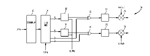
FIG. 3 shows an embodiment of a MOK system 30 using modulators 32 and
34 to produce length 8 codes in response to 3 information bits from the serial
to
parallel converter 14. In this embodiment, the set of orthogonal codes is the
length 8
Walsh code set, and the Walsh code set is modified using a complementary code.
The length 8 Walsh code set is:
1 1 1 1 1 1 1 1
1 1 1 1 0 0 0 0
1 1 0 0 1 1 0 0
1 0 0 1 1 0 0 1
1 0 1 0 1 0 1 0
1 0 1 0 0 1 0 1
1 0 0 1 0 1 1 0
1 1 0 0 0 0 1 1
1o In previous systems, the Walsh codes are modified by an element by element
exclusive-or with the code { 1 1 1 1 1 1 0 0}, so the last two chips of each
Walsh code
(or the chips of the last two columns of the Walsh code set) are inverted.
This
modifying code, however, has auto-correlation sidelobes with a worst-case
magnitude
of 5 (using -1's for the 0's), which is an autocorrelation value greater than
one-half
the length of the 8 chip code and produces multipath performance problems.
Instead, in the embodiment of FIG. 3, the MOK system 30 uses (a) length 8
complementary code(s), for example the sequences { 1 1 1 0 1 1 0 1 } or { 1 1
1 0 1 0 1
1 }, to modify the length 8 Walsh code set. For the latter code, the modified
Walsh
code set appears as:
1 1 1 0 1 0 1 1
1 1 1 0 0 1 0 0
1 1 0 1 1 0 0 0
CA 02261826 1999-02-15
9
1 0 0 1 1 0
0 1
1 1 1 1 1 1
0 0
1 1 1 0 0 0
0 1
1 0 0 0 0 1
0 0
1 0 1 0 1 1
1 1
This modified Walsh code set produces worst-case autocorrelation sidelobes
having a
magnitude or value of only 2. As such, this modified code compares favorably
in
performance to complementary Barker codes which have autocorrelation sidelobes
bounded to only one. Complementary Barker codes are discussed in Robert L.
Frank,
"Polyphase Complementary Codes." IEEE Transactions On Information Theory,
Vol. IT-26, No. 6, Nov. 1980, pp.641-647. However, Barker codes or sequences
only
exist for certain odd lengths such as length 11. The first of the two
complementary
codes specifically mentioned above has improved cross-correlation properties
for
1 o time shifted codes.
In the operation of the embodiment of FIG. 3, the scrambler 12 receives data
and scrambles the data according to the IEEE 802.11 standard. In other
embodiments, the scrambler 12 may not be necessary, and the data can be
manipulated by some other form of data conversion, interleaving or
modification, or
the data can be fed directly into the serial-to-parallel converter 14. In this
embodiment, the serial-to-parallel converter 14 is a 1:8 multiplexes (MUX)
which
produces a data symbol of 8 data bits in parallel according to a 1.375 MHz
clock
signal. The eight bit data symbol is encoded into a symbol comprising a I/Q
code
pair of 8 chip codes or codewords, so the symbol interval is equal to the code
length.
2o Three (3) of the bits of the data symbol are provided to the first
modulator 32 which
produces a corresponding length 8 Walsh code which has been modified by a
complementary code. The first modulator 32 produces the length 8 Walsh code at
a
chip rate of about 11 MHz as dictated by an 11 MHz clock signal. In the above
example, each symbol contains 8 data bits, which are encoded into independent
I and
Q codes of 8 chips. Chips are actually code bits, but they are called chips to
CA 02261826 1999-02-15
distinguish them from data bits. In this embodiment, the first modulator 32
corresponds to the I phase modulation branch of the MOK system 30 which
produces
the I component of the of the signal to be transmitted.
A second set of three (3) bits of the data symbol from the converter 14 is
provided to the second modulator 34 which produces a corresponding length 8
Walsh
code which has been modified using a complementary code. The second modulator
32 corresponds to the Q phase modulation branch of the MOK system 30 which
produces the Q component of the of the signal to be transmitted. In response
to the
three data bits, the second modulator 34 also produces a length 8 Walsh code
at a chip
1 o rate of about 11 MHz as dictated by the 11 MHz clock signal.
Of the remaining two of eight bits of the data symbol from the serial to
parallel converter 14, one is provided to a first XOR gate 36. If the bit is a
0, the first
XOR gate 36 changes the polarity of the length 8 Walsh code from the first
modulator
32. The resulting modified Walsh code Io"c is provided to signal circuitry 21
to
t 5 change any 0's to 1's and perform any additional signal processing and/or
conversion
before being provided to the first mixer 24 to modulate a Garner of frequency
w. The
last remaining bit is provided to a second XOR gate 38. If the bit is a 0, the
second
XOR gate 38 changes the polarity of the length 8 Walsh code from the second
modulator 34. The resulting modified Walsh code Qo"c is provided to the signal
2o circuitry 23 for any conversion and/or processing before being provided to
the second
mixer 26 to modulate a 90 degree shifted version of the carrier with frequency
w . If
instead of 0's, -1's are used, the first and second XOR gates 36 and 38, can
be
replaced by multipliers to change the polarity of Io"c and Qo"c. Subsequently,
the Io"c
modulated carrier and the Qo"c modulated carrier are combined and transmitted.
As
25 such, this particular embodiment of the MOK system 30 partitions 8 bits of
incoming
data into 4 bits for the I branch and 4 bits for the Q branch. The three data
bits on the
I branch are encoded into a code of 8 chips, and the three data bits on the Q
branch
are encoded in parallel into a code of 8 chips. Because the last two bits
encode
information by determining the polarity of the 8 bit symbols respectively, the
MOK
3o system 30 encodes 8 data bits into 2 codes which are both picked from a set
of 16
CA 02261826 1999-02-15
11
possible codes. In this example, there are 8 modified Walsh codes, which can
be
inverted to get 16 codes. With a symbol rate of 1.375 MSps and 8 bits/symbol,
the
data rate for the MOK system 30 is 1 lMBps.
FIG. 4 shows a graphical comparison of the packet error ratio v. delay spread
(ns) in multipath fading channels using 8 bits per symbol at 11 Mbps and a 4
taps
channel matched filter as would be understood by one of ordinary skill in the
art.
Curve 40 corresponds to digital modulation using Walsh codes modified by the
cover
sequence ( 11111100) of current systems 40, and curve 42 corresponds to
digital
modulation using Walsh codes modified by a complementary code ( 11101 O 11 )
1 o according to the principles of the present invention. The channel model
used has an
exponentially decaying power delay profile and independent Rayleigh fading
paths.
FIG. 4 shows that by using the complementary code, the system can tolerate a
delay
spread that is about 50% larger ( curve 42) than for the other code (curve 40)
to
achieve a packet error ratio of 1 % or 10%.
FIG. 5 shows an embodiment of a MOK system 50 which can be used as a
fallback mode for the MOK system 30 (FIG. 3). Once again, the input data is
scrambled by the scrambler 12 according to the IEEE 802.11 standard. The data
is
provided to a serial to parallel converter 52. The serial to parallel
converter 52 in this
embodiment produces 5 bit data symbols in parallel at a data symbol rate of
1.375
2o MSps. From the 5 bit data symbol, three bits are received by a modulator 54
which
encodes the 3 bits into a length 8 modified Walsh code according to the
principles of
the present invention. The length 8 modified Walsh code is provided to both I
and Q
branches 56 and 58. In accordance with another inventive aspect of this
particular
embodiment, by providing the same code to multiple phase modulation paths or
branches, this embodiment allows a fallback mode with independent phase
modulation, such as quadrature phase shift keying (QPSK) or 8-phase shift
keying (8-
PSK), of the same code on the multiple phase modulation paths, such as the I
and Q
branches 56 and 58 in this embodiment. On the I branch 56, the 8 chip modified
Walsh code is serially provided to a first XOR gate 60, and on the Q branch
58, the 8
3o chip Walsh code is serially provided to a second XOR gate 62. Of the two
remaining
CA 02261826 1999-02-15
12
bits from the serial to parallel converter 52, one bit goes to the first XOR
gate 60 to
adjust the polarity of the length 8 modified Walsh code and produce Io"t on
the I
branch 56, and the other bit goes to the second XOR gate 62 to adjust the
polarity of
the length 8 modified Walsh code and produce Qo"~ on the Q branch 58.
Depending
on the implementation, if -1's are used instead of 0's, the first and second
XOR gates
60 and 62 can be replaced by multipliers. As such, given data symbols of 5
bits/symbol and a symbol rate of 1.375 MBps, this embodiment provides a data
rate
of 6.8MBps.
FIG. 6 shows a graphical comparison of the packet error ratio v. delay spread
(ns) in multipath fading channels using 1 ) Walsh codes modified by the cover
sequence (11111100) of current systems with quadrature phase shift keying
(QPSK)
at a fallback rate of 6.8 Mbps (curve 63), 2) Walsh codes modified by a
complementary code (for example, 111 O 1 O 11 ) using 8-phase shift keying (8-
PSK) at
8.25 Mbps (curve 64), and 3) Walsh codes modified by a complementary code (for
example, 111 O 1 O 11 ) using QPSK at a fallback rate of 6.8 Mbps and the same
code on
I and Q branches (curve 65). The channel model used has an exponentially
decaying
power delay profile and independent Rayleigh fading paths. FIG. 6 shows that
the
delay spread tolerance is more than doubled by using the codes proposed by the
invention. Additionally, FIG. 6 shows that the digital modulation system can
be used
2o with alternative modulation schemes, such as 8-PSK instead of QPSK, to get
a higher
data rate (8.25 Mbps) without losing much delay spread performance as would be
understood by one of skill in the art.
FIG. 7 shows an embodiment of a MOK system 66 which can be used as a
fallback mode for the MOK system 30 (FIG. 3). The input data is scrambled by
the
scrambler 12 according to the IEEE 802.11 standard. The scrambled data is
provided
to a serial to parallel converter 68. The serial to parallel converter 68 in
this
embodiment produces 4 bit data symbols in parallel at a symbol rate of 1.375
MSps.
From the 4 bit data symbol, three bits are received by a modulator 70 which
encodes
the 3 bits into a length 8 modified Walsh code according to the principles of
the
3o present invention. The modulator 70 serially produces the length 8 Walsh
code at a
CA 02261826 1999-02-15
13
rate of I 1 MHz. The length 8 modified Walsh code is provided to an XOR gate
72
corresponding to both the I and Q branches. The length 8 modified Walsh code
is
multiplied by the remaining bit of the data symbol from the serial-to-parallel
converter 68 to adjust the polarity of the length 8 code and produce Io", and
Qo", in
serial form. Depending on the implementation, if -1's are used instead of 0's,
the
XOR gate 72 can be replaced by a multiplier. As such, given data symbols of 4
bits/symbol and a symbol rate of 1.375 MBps, this embodiment provides a data
rate
of S.SMBps.
FIG. 8 shows a digital demodulation system 76 which can be used at a
l0 receiver (not shown) to receive transmitted codes from a transmitter (not
shown)
using an embodiment of the digital modulation system described above. The
digital
demodulation system 76 receives a modified orthogonal code according to the
principles of the present invention. In response to the modified orthogonal
code, the
digital demodulation system produces a corresponding data symbol. Depending on
the particular implementation, the code chips and/or the data bits can be in
parallel or
m senes.
FIG. 9 shows a demodulation system 80 using the digital demodulation
system according to the principles of the present invention. In this
particular
embodiment, the received signal is supplied to both I and Q branches 82 and 84
of the
2o demodulation system 80. A first mixer 86 multiplies the received signal by
the coswt,
where c~ is the Garner frequency, to extract the modulated I information, and
a second
mixer 88 multiplies the received signal by sin wt to extract the modulated Q
information. After low pass filtering, the I and Q information are provided to
correlator blocks 90 and 92, respectively. In this particular embodiment, the
correlator blocks 90 and 92 contain 8 correlators for correlating time delayed
versions
of the I information and the Q information, respectively. The find code blocks
94 and
96 find the known modified orthogonal codes according to the present invention
which give the highest correlation magnitudes for the I and Q information. In
certain
embodiments, the demodulator 76 (FIG. 8) or portions thereof can be performed
in or
3o receive the output from the find code blocks 94 and 96 to decode the known
CA 02261826 1999-02-15
14
orthogonal codes into corresponding data bits. Depending on the embodiment,
the
digital demodulation system 76 (FIG. 8) or portions thereof can be implemented
in
the find code blocks 94 and 96, in the detect polarity blocks 98 and 100,
branching off
of the of the I and Q paths 82 and 84 and/or at the output of detect polarity
blocks 98
and 100 to decode the modified orthogonal codes to produce the corresponding
data
bits. In this embodiment, the detect polarity blocks 98 and 100 each decode an
additional data bit each from the polarity of the found modified orthogonal
code.
FIG. 10 shows an embodiment of a demodulation system 110 which can be
used at the fallback rate for the demodulator system 80 (FIG. 9) receiving
code
l0 symbols from the modulator system 50 (FIG. 5) where the same code is
transmitted
on multiple modulation paths. The difference between the demodulation system
110
and the full rate demodulation system of FIG. 9 is that the code detection
block 112
adds the squared correlation outputs of the I and Q correlators 90 and 92 and
detects
the modified orthogonal code according to the present invention which gave the
highest correlation complex magnitude. In accordance with an inventive aspect
of
this particular embodiment, the same code is on both the I and Q paths 82 and
84 for
digital demodulation. In this particular embodiment, a block 114 finds the
modified
orthogonal code with the highest complex correlation magnitude. In certain
embodiments, the demodulator 76 or portions thereof can be performed in or
receive
2o the output from the find code block 112 to decode the modified orthogonal
codes into
corresponding data bits. Depending on the embodiment, the digital demodulation
system 76 (FIG. 8) or portions thereof can be implemented in the code
detection
block 112, in a phase detector 114, branching off of the path 115 and/or at
the output
of the phase detector 114 to decode the modified orthogonal codes and produce
the
corresponding data bits. The phase detector 114 detects the phase of the
complex
correlation output to decode an extra 2 bits per code symbol for QPSK or an
extra 3
bits per code symbol for 8-PSK.
In addition to the embodiment described above, alternative configurations of
the digital (de)modulation system according to the principles of the present
invention
3o are possible which omit and/or add components and/or use variations or
portions of
CA 02261826 1999-02-15
the described system. For example, the above applications use a Quadrature
Phase
Shift Keying (QPSK) phase shift modulation scheme (FIG. 1, 3, 5) along with
the
digital modulation scheme and a binary phase shift keying (BPSK) scheme (FIG.
6),
but the digital modulation system can be used with other modulation schemes,
such as
5 amplitude modulation including quadrature amplitude modulation (QAM) and
other
phase modulation schemes including 8-phase shift keying (8-PSK) as would be
understood by one of ordinary skill in the art. Additionally, The digital
modulation
system has been described as using orthogonal codes of 1's and 0's which are
modified by codes of 1's and 0's, but the digital modulation system can be
performed
t0 using codes of 1's and -1's or 1's and 0's depending on the embodiment. In
the
embodiments described above, codes of 1's and -1's are received at the
receiver, and
the correlation determinations are described in terms of 1's and -1's, but the
demodulation system can use 1's and 0's or 1's and -1's depending on the
embodiment.
t 5 Furthermore, the digital modulation system has been described using a
particular configuration of distinct components, but the digital modulation
system can
be performed in different configurations and in conjunction with other
processes.
Additionally, the various components making up the digital modulation system
and
their respective operating parameters and characteristics should be properly
matched
2o up with the operating environment to provide proper operation. It should
also be
understood that the digital modulation system and portions thereof can be
implemented in application specific integrated circuits, software-driven
processing
circuitry, firmware, lookup-tables or other arrangements of discrete
components as
would be understood by one of ordinary skill in the art with the benefit of
this
disclosure. What has been described is merely illustrative of the application
of the
principles of the present invention. Those skilled in the art will readily
recognize that
these and various other modifications, arrangements and methods can be made to
the
present invention without strictly following the exemplary applications
illustrated and
described herein and without departing from the spirit and scope of the
present
invention.