Note: Descriptions are shown in the official language in which they were submitted.
CA 02261840 1999-02-15
SERIAL DATA TRANSFER PROCESS. AND SYNCHRONOUS SERIAL BUS
INTERFACE IMPLEMENTING SUCH PROCESS
The present invention relates to the area of serial digital data
transmissions. It relates more particularly to a synchronous bus and its
s master/slave transmission protocol between a main processing unit (master)
and a peripheral unit (slave).
An example of such a bus, used in different categories of
equipment, is the so-called IZC bus described in European patent 0 051 332. A
certain number of clock cycles are required for the microprocessor or
i o microcontroller constituting the main processing unit to retrieve one byte
of
data (58 clock cycles in the case of the circuit marketed by the PHILIPS
company with the reference number PCD 3316 which employs such a bus).
An object of the present invention is to propose a new synchronous
serial bus protocol enabling faster access to certain data in the peripheral
unit.
~s The invention thus proposes a process for serial data transfer
between a main processing unit and a peripheral unit connected to each other
by a bus including a data line and a clock line,
wherein the main processing unit controls synchronised transfer
cycles by means of the clock line, including transfer cycles with addressing
2o and direct transfer cycles,
wherein, during each cycle, the main processing unit transmits on
the data line a strobe pulse while the clock line is at a first logic level,
CA 02261840 1999-02-15
-2 -
wherein, before transmitting the strobe pulse in a transfer cycle with
addressing, the main processing unit transmits on the data line bits of a
transfer address, with corresponding synchronisation pulses on the clock line,
wherein, after receiving the strobe pulse in a transfer cycle with
addressing, the peripheral unit accesses to a memory location determined
from the transfer address to write or read data bits successively presented on
the data line synchronously with corresponding synchronisation pulses on the
clock line,
and wherein, after receiving the strobe pulse in a direct transfer
cycle, the peripheral unit accesses to a memory location determined prior to
said direct transfer cycle to write or read data bits successively presented
on
the data line synchronously with corresponding synchronisation pulses on the
clock line.
The transfer protocol is very simple, thus enabling fast access. It is
~5 based on the detection of the strobe pulse on the data line by the
peripheral
unit. The main processing unit distinguishes between the different transfer
modes through the position of this strobe pulse during the cycle, andlor by
means of selection bits provided on the data line before the strobe pulse
and/or by a decoding of the address bits.
2o Very fast access to some storage locations in the peripheral unit is
made possible by the direct transfer mode, given that the main processing unit
provides no address bits in this mode, and that the desired data is previously
selected.
CA 02261840 1999-02-15
-3-
The location where the transmitted data bits are obtained in direct
transfer mode may be a predetermined fixed location, which enables the
structure of the bus interface of the peripheral unit to be simplified to the
maximum and therefore its cost to be minii~nised.
It may also be a location whose address is obtained from data
supplied by the main processing unit during a previous write cycle. In this
case, direct read cycles can be run by the main processing unit to read
different types of data in the peripheral unit. The number of bits read in
this
way may also be a parameter set by the main processing unit during a
previous write cycle.
The direct read mode may particularly be used in the fast handling
of some interrupts by the main processing unit.
Another advantage of the proposed bus is that it may share its data
line and its clock line with those of a bus operating in accordance with
another
~ s protocol for the exchange of data between the main processing unit and
other
entities.
According to another aspect, the present invention proposes a
synchronous serial bus interface for a peripheral unit controlled by a main
processing unit by means of a bus including a data line and a clock line
2o including:
- strobe pulse detection means, to detect strobe pulses occurring
on the data line of the bus, while the clock line of the bus is at a first
logic
level;
CA 02261840 1999-02-15
-4 -
- a first shift register timed by the clock line of the bus, having a
serial data input connected to the data line;
- a second shift register having a serial data input connected to the
serial data output of the first shift register or to the data line, and timed
by the
s output of an EXCLUSIVE OR gate having an input connected to the clock line
of the bus, and another input receiving a binary selection signal;
- an output switch connected on the one hand to the serial data
output of the second shift register and on the other hand to the data line of
the
bus;
- transfer cycle identification means, in order to analyse the content
of the first shift register when a strobe pulse is detected so as to identify
each
transfer cycle to which a detected strobe pulse belongs;
- write registers addressable from a write address obtained from the
first shift register when a write cycle with addressing has been identified, a
~ 5 write cycle with addressing wherein the binary selection signal is held at
0, the
output switch is kept open and the detection of the strobe pulse is followed
by
the parallel transfer of the content of the second shift register into the
write
register denoted by the write address;
- read registers addressable from a read address when a read cycle
2o has been identified, a read cycle wherein the detection of the strobe pulse
is
followed by the parallel transfer of at least part of the content of the read
register denoted by the read address into the second shift register and by the
serial transfer of the content of the second shift register to the output
switch, a
CA 02261840 1999-02-15
-5-
serial transfer during which the binary selection signal is set at 1 and the
output switch is closed; and
- transfer cycle managing means to obtain the read address from
the first shift register when a read cycle with addressing has been
identified,
s and to supply a previously specified read address when a direct read cycle
has
been identified.
Other features and advantages of the present invention will emerge
in the following description of non-restrictive embodiments, by reference to
the
appended drawings, wherein:
- figure 1 is a block diagram of a device implementing the present
invention;
- figures 2 to 4 are timing diagrams showing respectively a write
cycle, a read cycle with addressing and a direct read cycle run in an example
of the process in accordance with the invention;
~s - figure 5 is a diagram of an example of an inputloutput module of an
interface implementing such process;
- figure 6 is a diagram giving details of an embodiment of a strobe
detector of the module in figure 5;
- figure 7 is a diagram of another example of an inputloutput module
20 of an interface in accordance with the invention;
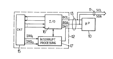
Figure 1 shows diagrammatically a device the general operation of
which is controlled by a main processing unit constituted by a microprocessor
10. The microprocessor 10 controls a certain number of units (not shown) of
the device by means of a serial bus 11 of known type, such as for example a
CA 02261840 1999-02-15
-6 -
IZC bus comprising a data line SDA and a clock line SCL (see EP-B-0 051
332).
Another peripheral unit 12 is controlled by the microprocessor 10 by
means of a serial bus 13 operating in accordance with the invention.
s As an example of application, the device may be a telephone whose
microprocessor 10 controls, by means of an 12C bus 11, units such as a
keyboard, a display screen and different interfaces, the unit 12 being a
component dedicated to the observation of the telephone line and to the
processing of certain data relative to sophisticated services offered by
network
operators.
In this kind of application, the cost of the components must be as
low as possible, and it is particularly desirable to be able to reduce as far
as
possible the number of inputloutput pins in the microprocessor. To this end,
the bus 13 serving as interchange between the units 10 and 12 borrows the
~s data and clock lines of the general bus 11, which are also denoted BDA and
BCL. The protocol which will be described below prevents ambiguities on
these lines.
The bus 13 additionally comprises an interrupt line INT enabling the
peripheral unit 12 to indicate certain events to the microprocessor 10 by
2o sending an interrupt request.
The bus interface, provided between the operating circuits 15 of the
peripheral unit 12 and the bus 13, includes an input/output module 16 and an
interrupt processing module 17. The module 17 receives from the circuits 15
respective interrupt signals IRQ, - IRQ~ relative to a group of n events whose
CA 02261840 1999-02-15
-7-
detection triggers the sending of an interrupt request on the INT line. The
module 17 controls the storage, in a status register of the module 16, of n
bits
corresponding to the statuses of the signals IRQ, - IRQ~ . In response to an
interrupt request received on the INT line, the microprocessor 10 reads the
status register to discover the origin of the interrupt and to determine which
interrupt program should be run.
In the example of application to a telephone, the group of events
associated with the interrupt signals IRQ, - IRQ~ includes for example the
detection of ringing on the line, the detection of the presence of line
voltage
and the detection of various signals transmitted by the network on the
telephone line in the context of particular services.
The first two lines in figures 2 to 4 show how the microprocessor 10
controls the lines BCL, BDA of the bus 13 to trigger data transfers from or to
the peripheral unit 12. In each case, the use of the bus 13 is signalled by a
~5 strobe pulse presented during a transfer cycle on the data line BDA while
the
clock line BCL is at a given logic level. In the example described, this logic
level is level 1, and the strobe pulse is a logic level 0, i.e. starting with
a falling
edge and ending with a rising edge, these two edges occurring while BCL=1.
In a write cycle with addressing (figure 2), the strobe pulse is
2o preceded by n+m+1 regular synchronisation pulses on the clock line BCL (n=8
and m=4 in the example shown), each pulse starting with a rising edge and
ending with a falling edge. The changes in logic level on the data line BDA
are
not authorised during these n+m+1 synchronisation pulses (BCL=1 ), but only
between these pulses (BCL=0). The first n=8 bits transmitted during the write
CA 02261840 1999-02-15
_8 _
cycle are data bits forming a byte to be written, transmitted by the
microprocessor 10 in descending order of significance D7-D0. The following
m=4 bits A3-AO form a write address for storing the previous byte. The final
bit
RW, which immediately precedes the strobe pulse, indicates by the value
RW=0 that the current cycle is a write cycle.
In a read cycle with addressing (figure 3), the strobe pulse is
preceded by m+1 synchronisation pulses on the clock line BCL, m+1 bits being
transmitted as previously by the microprocessor on the data fine BDA. The
first
m=4 of these bits form a read address A3-AO for the data required by the
~ o microprocessor. The final bit RW, which immediately precedes the strobe
pulse, indicates by the value RW=1 that the current cycle is a read cycle with
addressing.
After the strobe pulse in a read cycle with addressing, the
microprocessor 10 still transmits n=8 synchronisation pulses on the line BCL,
~ 5 to which the module 16 of the peripheral unit 12 responds by presenting
successively on the line BDA the n=8 bits of the read byte, in descending
order
of significance D7-D0. As previously, the transmission of these n data bits is
operated such that transitions between these bits occur when the clock line is
in the status BCL=0.
2o In a direct read cycle (figure 4), the strobe pulse is transmitted by
the microprocessor at the beginning of the cycle. After this strobe pulse, the
processor 10 provides p synchronisation pulses on the clock line BCL, to
which the peripheral unit 12 responds by transmitting p data bits d1-d0 on the
CA 02261840 1999-02-15
_g_
line BDA in the same way as previously (the transitions between bits occur
while BCL=0).
In the example of figure 4, the particular case where p=2 has been
shown. The p=2 bits d1-d0 are for example read from a predetermined fixed
address in the registers 16 of the input/output module.
In the example of application to the telephone, the p=2 bits read in a
direct read cycle may be the two bits of the status register indicating
respectively the detection of ringing on the telephone line and the presence
of
line voltage. These two bits represent data which the microprocessor 10 may
~ o need very urgently in order to adopt an appropriate response. Thus, when
it
receives an interrupt request on the INT line, the microprocessor 10 may
trigger a direct read cycle with a very fast run time, so as to discover the
values of these two bits and to adopt the appropriate response in the shortest
possible time if they do in fact show the origin of the interrupt. In the
opposite
~ 5 case, the microprocessor 10 may then trigger a read cycle with addressing
in
the status register so as to discover the other status bits and to identify
the
origin of the interrupt.
As a numerical example (see figure 2), the clock frequency being
500 kHz, the length of the pulses on the clock line (BCL=1 ) may be T1=1 ~.s,
2o and these pulses may be separated by a length T2=1 ~,s (BCL=0); the logic
level 0 strobe pulse may have a length T3=1 ~s, preceded and followed by a
standby time T4=0~5 ~s during which BCL=BDA=1. The length of a write or
read cycle with addressing is then about 15 ~,s, and the length a direct read
cycle with p=2 is about 4 ~,s. Access may be even faster when the bus is not
CA 02261840 1999-02-15
-10-
subject to the constraints of the IzC protocol, the clock frequency being able
in
this case to be higher.
When it is not running a transfer cycle on the bus 11113, the
microprocessor 10 keeps the clock line SDA/BDA at logic level 1.
In the IZC bus protocol 11, a falling edge on the data line SDA while
the clock line SCL is at logic level 1 characterises a transfer cycle start,
whereas a rising edge f on the data line SDA while BCL=1 characterises a
transfer cycle end (figure 4). As a result, according to this 12C protocol,
the
data line does not change logic level more than once while the clock line is
at
level 1. It can therefore be seen that the transfer protocol proposed
according
to the invention, shown by the figures 2 to 4, gives rise to no ambiguity with
the
12C bus protocol used by the microprocessor 10 to control other units of the
device:
- control of the SDA/BDA, SCUBCL lines belongs to the
~ s microprocessor 10 which ensures the coexistence of the two buses:
- when the microprocessor controls the bus 13 as shown in one of
figures 2 to 4, no IzC transfer cycle is run on the bus 11 since the strobe
pulse
leads to starting and then ending an 12C cycle wherein nothing would have
occurred, and the stability of the data line BDA while BCL=1 outside the
strobe
2o pulse cannot generate any 12C cycle start;
- during the run of a transfer cycle in accordance with the IZC
protocol, the strobe pulse is not received by the peripheral unit 12 with the
result that untimely transfers on the bus 13 are avoided.
CA 02261840 1999-02-15
-11 -
The structure of the input/output module 16 of the peripheral unit 12
is for example in accordance with the diagram in figure 5. In this figure, the
reference 18 denotes a group of M<_2m registers of n bits wherein the
microprocessor 10 may control writes in cycles such as that shown in figure 2,
s the register of the group 18 where such a write occurs being selected by
means of the write address A3-A0. The reference 19 denotes a group of
M'<_2"' registers of n bits wherein the microprocessor 10 may control data
reads in read cycles with addressing such as that shown in figure 3, the
register of the group 19 where such a read occurs being selected by means of
the read address A3-A0. These read registers 19 include the status register
used for the management of interrupts.
The module 16 includes a shift register consisting of m+1 cascaded
D flip-flops 20o-20m timed by the rising edges of the signal present on the
clock line BCL. The data input of this shift register, i.e. the D input of the
first
~ s flip-flop 200, is connected to the data line BDA. The module 16 includes a
second shift register consisting of n cascaded D flip-flops 20m+~-20m+n timed
by the rising edges of a signal CC delivered by an EXCLUSIVE OR gate 21.
For 1 <_i<_m+n, the D input of flip-flop 20~ is connected to the Q output of
flip-flop
20~-1, The gate 21 has an input connected to the clock line BCL. Its other
input
2o receives a binary selection signal CD.
Upon reception of a strobe pulse by the peripheral unit 12 in a write
or read cycle with addressing, the mode selection bit RW is present at the Q
CA 02261840 1999-02-15
-12-
output of flip-flop 200, and the m address bits A3-A0, are present at the Q
outputs of flip-flops 20~-20n.
An auxiliary register of m bits consists of m D flip-flops 22~-22m. For
1 <_i<_m, the D input of flip-flop 22~ is connected to the Q output of flip-
flop 20~.
s The Q outputs of flip-flops 22~-22m supply the m address bits delivered to
the
group of write registers 18 and to the group of read registers 19. For this
auxiliary register 22~-22m to receive the address A3-AO the moment the strobe
pulse is detected in a write or read cycle with addressing, the D flip-flops
22~-
22m are timed by the rising edges of a HOLD signal delivered by a strobe
detector 24.
This detector 24 (figure 6) includes two D flip-flops 25, 26 whose Q
outputs are reset to logic level 0 at each falling edge occurring on the clock
line BCL. The line BCL is connected to the D input of flip-flop 25 which is
timed
by the falling edges occurring on the data line BDA, and whose Q output
~ s delivers the aforementioned HOLD signal. This signal is on the one hand
addressed to the D input of flip-flop 26 timed by the rising edges occurring
on
the data line BDA, and whose Q output delivers a detection signal STRI. This
STRI signal has a logic level 1 pulse which starts at the end of each strobe
pulse and ends when the BCL line returns to 0.
2o An AND gate 28 combines the STRI signal with the logic
complement of the RW bit obtained on the Q output of flip-flop 200 to produce
the write control signal WR addressed to the group of write registers 18. This
signal WR (figure 2) controls the parallel transfer of the n bits D7-DO
present
CA 02261840 1999-02-15
-13-
on the Q outputs of flip-flops 20m+~-20m+n in the register of the group 18
whose location is denoted by the m address bits A3-AO obtained on the Q
outputs of flip-flops 22~-22m.
Another AND gate 29 receives the signal STRI and the selection bit
s RW obtained on the Q output of flip-flop 200 to produce a signal RR having a
similar behavior in the read cycles (figures 3 and 4).
In order to distinguish read cycles with addressing from direct read
cycles, provision is made for one value of the read address to be excluded by
the microprocessor 10 for the read cycles with addressing. As an example, this
may be the value for which all the address bits are at 1.
The flip-flops of the first shift register 200-20m each have a pre-
selection input P acting to force their Q output to logic level 1 upon each
falling
edge of a pre-selection signal CP. This signal CP is supplied by a filter
formed
by an AND gate 31 belonging to read cycle managing means 30. The AND
~ s gate 31 combines the following signals:
- a general reset signal RES for the unit 12;
- the logical complement of the write control signal WR, whose
rising edge, occurring at the end of a write cycle (figure 2), thus causes the
writing of the excluded address in flip-flops 2o~-20m of the first shift
register,
2o and of RW=1 in flip-flop 200;
- an end of read cycle signal EORC, which has a logic level 0 pulse
at the end of each read cycle (figures 3 and 4), to write RW=1 as well as the
excluded address in the register 200-20m at the end of each read cycle, direct
or with addressing; and
CA 02261840 1999-02-15
-14-
- a false strobe detection signal F, which locates logic level changes
on the data line BDA occurring while BCL=1 and which cannot be attributed to
a strobe pulse.
The signal F acts to force the writing of RW=1 and of the excluded
address value in the register 20o-20m at the end of the transfer cycles
controlled by the microprocessor 10 in accordance with the IZC protocol. This
signal F has a falling edge at the end of each IZC transfer cycle, as is shown
in
the left hand part of figure 4. This signal F is for example supplied by the
inverted output Q of a D flip-flop 27 of the strobe detector 24 (figure 6).
This
~ o flip-flop 27 is reset to 0 at each falling edge occurring on the clock
line BCL.
The line BCL is connected to the D input of flip-flop 27 which is timed by the
rising edges occurring on the data line BDA.
The shaping of the pre-selection signal CP is such that the
microprocessor 10 can decide at each moment to run a direct read cycle.
~5 To identify the nature of the current transfer cycle, the AND gates
28, 29 are completed by a detection logic 33 connected to the Q outputs of the
flip-flops of the auxiliary register 22~-22m. This detection logic 33, which
simply
consists of an AND gate with m inputs when the excluded address value is
11...1, delivers a selection bit FRM which is at 1 when the excluded address
is
2o detected and at 0 otherwise.
The read cycle managing means 30 further include an address
switch 34 controlled by the FRM bit, a timing module 35 and an address
management module 36. The module 35 delivers the read control signal RD
supplied to the group of registers 19. This signal RD is produced in response
CA 02261840 1999-02-15
-15-
to the pulse from the signal RR delivered by the AND gate 29, and
corresponds to that pulse prolonged during a clock cycle BCL, as figures 3 and
4 show.
A three-state gate 40 forms an output switch of the input/output
s module 16, with its input connected to the Q output of the last flip-flop
20m+n of
the second shift register, and its output connected to the data line BDA. This
three-state gate 40 may be controlled by the binary selection signal CD which
is supplied to the EXCLUSIVE OR gate 21, so as to be in the off (open) state
when CD=0 and in the on (closed) state when CD=1.
The signal CD is delivered by the timing module 35. It remains at
level 0 outside transfer cycles on the bus 13 as well as during write cycles.
During a read cycle (figures 3 and 4), the signal CD remains at level 0 until
the
strobe pulse is detected. When it senses a rising edge on the output RR of the
gate 29, the module 35 generates a rising edge of the signal CD which is then
~ s held at 1 until the end of the following synchronisation pulses on the
clock line
BCL. The module 35 therefore holds the signal CD at 1 until it has received n
synchronisation pulses on the line BCL when FRM=0, and until it has received
p synchronisation pulses when FRM=1. The level 0 pulse of the end of cycle
signal EORC is produced when the signal CD returns to 0 (figures 3 and 4).
2o When FRM=0, the switch 34 is in the position shown in figure 5, so
that a pulse of the RD signal causes the reading of a byte in the group 19 at
the address present in the auxiliary register 22~-22m. The circular shift
module
38 to which the bits of the byte read in the group 19 are supplied is
deactivated
when FRM=0, which enables the parallel transfer of these bits to the shift
CA 02261840 1999-02-15
-16-
register 20m+~-20m+~. The most significant bit in the byte is supplied first
on
the data line BDA via the gate 40, whereas the other bits of the byte are
loaded in the flip-flops 20m+2-20m+~ of the second shift register. These other
bits are then delivered in series on the data line BDA in response to the
following synchronisation pulses of the clock BCL. The inversion of this clock
by the exclusive OR gate 21 enables data stability to be ensured in time
intervals when BCL=1.
In a direct read cycle, the switch 34 is positioned to obtain the read
address a from the address management module 36. When this address a is
fixed, the module 36 is reduced to connections supplying the constant value a
to the switch 34. If the p bits read in a direct read cycle are always the
most
significant p bits of one of the group 19 registers, the shift module 38 is
useless. Othenivise, it is activated by the FRM=1 bit so as to introduce the
required shift, of ~ bits, to deliver the required bits to the data line BDA.
~ 5 It is possible to choose, for the number of bits to be transferred in a
direct read cycle, a number p greater than the size n of the group 19
registers.
The operation is then the same as that described previously, except that the
timing module 35 has to reactivate the read control signal RD every n
synchronisation pulses thus causing the incrementation of the address
2o supplied by the module 36 (essentially consisting of a counter), and the
parallel transfer to the shift register 20m+~-20m+n of the content of a new
register of the group 19 pointed to by the incremented address.
The parameters p (number of bits transferred in a direct read cycle),
a (start address) and 8 (possible shift) may be fixed, as in the previously
CA 02261840 1999-02-15
-17-
described example. They may also be parameters which can be programmed
by the microprocessor 10. In this case, the modules 35, 36 and 38, which use
parameters p, a and 8 respectively, obtain them from one of the write
registers
of the group 18. To modify one or other of these parameters, the
microprocessor 10 may simply run a write cycle in the register or registers in
question, the addresses of which it knows.
In the alternative embodiment shown in figure 7, the direct transfer
cycles, without addressing, are not limited to read cycles. Direct write
cycles
are also possible. In addition, in that embodiment, the mode selection bit RW
is not transmitted by the microprocessor. The distinction between the read and
write cycles is carried out on the basis of a decoding of the addresses
present
in the auxiliary register 22~-22m upon the detection of the strobe pulse.
The input-output module shown in figure 7 has numerous elements
in common with that of figure 5, which are designated by the same reference
~ s numerals. The first shift register whose input is connected to the data
line BDA
of the bus 13 lacks one flip-flop since the RW bit no more needs to be taken
into account. The flip-flops 20~-20m remain and are coupled in the same way
to the flip-flops 22~-22m of the auxiliary register.
The parallel m-bit output of the auxiliary register is connected to a
2o cycle type detection logic 50, which also receives the STRI signal output
by
the strobe detector 24. Logic 50 performs a decoding of the addresses
contained in the auxiliary register 22~-22m when it receives a pulse of the
STRI signal. This decoding is in accordance with predefined rules. By way of
non-restrictive example, those rules may consist in that (i) the addresses
CA 02261840 1999-02-15
-18-
having the form 1xx...x (where each x is 0 or 1 ) are used by the
microprocessor in read cycles with addressing, (ii) the addresses having
performed 0xx...x are used in the write cycles with addressing, (iii) the
address
111...1 is an excluded read address, whose presence in the auxiliary register
s 22~-22m characterises a direct to read cycle, and (iv) the address 011...1
is an
excluded write address whose presence in the register 22~-22m characterises
a direct write cycle. In this particular case, there are as many read-
addressable
locations as write-addressable locations. A decoding table (possibly
programmable by the microprocessor 10) in logic 50 more generally permits
any combination of memory areas accessible in read andlor write cycles.
Upon detection of a read cycle (direct or with addressing), the logic
50 produces a logic level 1 pulse in the RR signal whose role is the same as
that described in the preceding embodiment (see figures 9 and 10). Upon
detection of a write cycle (direct or with addressing), the logic 50 likewise
~ s produces a logic level 1 pulse in the WW signal, as indicated in figures 8
and
11. In each direct transfer cycle, the logic 50 further activates a signal FM,
whose role is similar to that of the FRM signal in the preceding embodiment
(in
particular, it controls the address switch 34 which delivers the read or write
address A, and possibly the shift module 38).
2o As illustrated in figure 7, the detection logic 50 could further produce
control signals C 1, C2, ... responsive to the detection of certain particular
addresses in the auxiliary register 22~-22m. This type of decoding offers the
possibility to transmit controls to certain elements of the peripheral unit 12
without having to explicitly transfer data on the line BDA.
CA 02261840 1999-02-15
-19-
The signals FM, RR and WW output by the detection logic 50 are
supplied to a transfer timing module 52 forming part of the transfer cycle
management means 30, and playing a role similar to that of module 35
described with reference to figure 5. This module 52 produces the read control
s signal RD and write control signal WR supplied to the register arrays 19,18.
The production of the signals RD, CD and EORC by module 52 is identical to
that previously described (figures 9 and 10).
The production of the write control signal WR takes into account the
fact that, in the considered alternative embodiment, the written data D7-DO or
d1-d0 are transmitted on the data line BDA by the microprocessor 10 after the
strobe pulse. In a write cycle with addressing (FM=0), the module 52 thus
delays by n cycles of the clock BCL the activation of the WR signal (figure
8).
In the case of a direct write cycle, this delay is of p cycles of the clock
BCL
(figure 11 ).
~ s In order to allow for the loading of the data bits to be written into the
second register 20m+~-20m+n, the serial input of that register, consisting of
the
D input of flip-flop 20m+1 is directly connected to the data line BDA, as
shown
in figure 7. In another alternative embodiment, the D input of flip-flop 20m+~
could be connected either to the Q output of flip-flop 20m or to the data line
2o BDA depending on the position of a switch. This switch could for instance
be
controlled by a control bit C1 or C2 output by the detection logic 50 in
response to a coded command from the microprocessor 10, thereby enabling
the processor 10 to dynamically decide whether it transmits the data before or
after the strobe pulse in the write cycles.
CA 02261840 1999-02-15
- 20 -
As shown in figure 11 in the particular case considered hereabove
for the coding of the addresses, the microprocessor 10 provides a bit at 0 on
the data line BDA at the same time as it produces a clock cycle on the line
BCL immediately before transmitting the strobe pulse in the direct write
cycles.
s This allows for the loading of a bit 0 in the flip-flops 20~ and 22~, so as
to
change the default address 111...1 characterising the direct read cycles into
the address 011...1 characterising the direct write cycles, whereby the
detection logic 50 can then perform the suitable decoding.
If the number p of bits concerned by a direct transfer (read or write)
cycle is greater than the size n of a register of the arrays 18,19, the
control
signal RD or WR is periodically reactivated as in the preceding example, and
the address counter 36 is incremented by the output of an OR gate 54
receiving the signals RD and WR. The microprocessor may thus have access
to several registers during the same direct transfer cycle.
~ 5 Provision may also be made for a shift 8 in the position of the bits
concerned by a direct write cycle. For this, a circular shift module 56,
controlled by the FM bit in the same manner as module 38, is provided
between the register 20m+~-20m+~ and the write register array 18.This module
56 also receives the number p of bits concerned by the direct write cycle, so
as
2o to inhibit the write operation in the non-concerned locations of the
addressed
register.