Note: Descriptions are shown in the official language in which they were submitted.
CA 02262357 2001-09-11
DIELECTRIC RESONANT HAVING A COUPLING LINE FORMED
THEREON
BACKGROUND OF THE INVENTION
1. Field of the Invention
The present invention relates to a dielectric resonant apparatus, and
more particularly to a dielectric resonant apparatus for use in the
microwave or millimeter wave range.
2. Description of the Related Art
A dielectric resonator having low phase noise and high stability of
resonant frequency is used as a resonator or in an oscillator in a high-
frequency range such as a microwave or millimeter wave range.
In Laid-open Japanese Patent Application No. 8-265015, the
assignee of the present application has presented a module in which
electrodes are arranged on both main surfaces of a dielectric sheet to form
a dielectric resonator on a part of the sheet. The electrodes arranged on
the dielectric sheet serve as ground potentials; and a microstrip arranged
on another dielectric sheet is stacked
CA 02262357 2001-09-11
2
on the dielectric sheet. This arrangement is used in a high-frequency
module such as a VCO.
In addition, a similar type of high-frequency module has been
presented in Japanese Patent Application No. 8-294087 (Publication No.
10-145117), published May 29, 1998 and U.S. Patent No. 6,016,090,
issued January 18, 2000 to lio et al. Figs. 19 and 20 illustrate the structure
of the high-frequency module. It should be noted that this high-frequency
module was not laid-open to the public at the time of filing of the Japanese
Application No. 10-42017 on which the present application is based. Thus,
the inventors do not deem the high-frequency module of Figs. 19-20 to be
prior art with respect to the present invention.
In Fig. 19, reference numeral 1 denotes a dielectric sheet. An
electrode is formed on each of two main surfaces of the dielectric sheet 1.
Each electrode has an opening formed at a location corresponding to the
location of the opening of the other electrode (reference numeral 4 denotes
one opening). The part defined by the electrode openings serves as a
dielectric resonator. A circuit board 6, on a surface of which a circuit
including microstrip lines is formed, is placed on the upper surface of the
dielectric sheet 1. On the circuit board 6, there are also provided coupling
lines 11 and 12 at locations which allow the coupling lines 11 and 12 to be
coupled with the dielectric resonator formed in the electrode openings 4.
CA 02262357 1999-02-23
- 3 -
In the example shown in Fig. 20, electrodes each
having an opening formed at locations corresponding to each
other (reference numeral 5 denotes an opening formed in one
electrode) are disposed on two respective main surfaces of a
dielectric sheet 1 such that the part defined by the
electrode openings serves as a dielectric resonator. The
dielectric sheet 1 is placed on a circuit board 6 such that
the dielectric resonator is coupled with a transmission line
formed on the circuit board 6. A spacer is disposed between
the dielectric sheet 1 and the circuit board 6 so that
electrodes on the lower surface, in Fig. 20, of the
dielectric sheet 1 are insulated from the electrodes on the
upper surface of the circuit board 6.
In dielectric resonators of the types described above
in which electrodes each having an opening formed at
locations corresponding to each other are disposed on
respective two main surfaces of a dielectric sheet, almost
all electromagnetic field is confined in the part defined by
the electrode openings and thus electromagnetic energy is
concentrated in that part. Therefore, strong coupling can
be achieved by placing the coupling line at a proper
location. Thus, the dielectric resonator can be used, for
example, to realize an oscillator having a large oscillation
frequency modulation width and/or large output power.
In the oscillators shown in Figs. 19 and 20, the
CA 02262357 1999-02-23
- 4 -
frequency modulation width varies depending on the external
Q (Qe2) of the resonant circuit (coupling line 12) as shown
in Fig. 16. As can be seen from Fig. 16, it is possible to
greatly increase the frequency modulation width by reducing
the external Q (Qe2).
Fig. 17 illustrates the relationship between the
reflection coefficient of the resonant circuit and the
external Q (Qel) of the dielectric resonator and the band-
reflection coupling line 11. From Fig. 17, it can be seen
that the reflection coefficient of the resonant circuit
increases if the external Q (Qel) is reduced. Because the
output increases with the increase in the reflection
coefficient of the resonant circuit, it is possible to
increase the output by reducing the external Q (Qel).
Fig. 2 illustrates an electromagnetic field
distribution in a dielectric resonator of the type in which
the resonator is formed on a dielectric sheet in the manner
described in Fig. 19 or 20. In Fig. 2, reference numerals 2
and 3 denote electrodes formed on the respective main
surfaces of the dielectric sheet 1. The part defined in the
circular openings 4 and 5 of the respective electrodes 2 and
3 serves as a TE010-mode dielectric resonator. In the
conventional resonant circuit for use in an oscillator, the
coupling lines 11 and 12 are disposed at locations slightly
apart from the surfaces of the electrode openings 4 and 5
CA 02262357 1999-02-23
- 5 -
(hereinafter referred to as electrode opening planes)
forming the dielectric resonator part. If the distance
between the coupling lines and the electrode opening plane
is increased, the electromagnetic field applied to the
coupling lines decreases rapidly as can be seen from Fig. 1.
This means that the degree of coupling decreases rapidly
with the increase in the distance between the coupling lines
and the electrode opening plane.
Fig. 18 illustrates the oscillation output as a
function of the distance between the coupling lines and the
electrode opening plane (wherein the distance is measured in
a direction perpendicular to the electrode opening plane).
As can be seen from Fig. 18, if the distance between the
coupling lines and the electrode opening plane is reduced,
then the external Q decreases and the output increases.
However, in the dielectric resonant apparatus shown in
Fig. 19 or 20, it is impossible to reduce the distance
between the coupling lines and the electrode opening to a
value smaller than a practical limit. That is, in the
example shown in Fig. 19, in order to decrease the distance
from the electrode opening plane of the electrode opening 4
to the coupling lines 11 and 12, it is required to decrease
the thickness of the circuit board 6 because the coupling
lines 11 and 12 are disposed on the upper surface of the
circuit board 6. However, the reduction in the thickness of
CA 02262357 1999-02-23
- 6 -
the circuit board 6 is limited to a practically-possible
minimum value. In the example shown in Fig. 20, it is
required to reduce the thickness of the spacer. However,
the spacer also has its minimum possible thickness. Besides,
the reduction in the thickness of the spacer results in
another problem that it becomes impossible to obtain a
desired characteristic because the reduction in the
thickness of the spacer produces a great change in the
characteristic impedance of the lines 11 and 12.
Still another problem is the positioning accuracy of
the coupling lines relative to the resonator. In the
millimeter range, a very small change in the location of the
coupling lines relative to the location of the resonator
results in a large change in the characteristic. Therefore,
high positioning accuracy is required. However, in the
conventional dielectric resonant apparatus, the resonator
and the coupling lines are produced separately by different
processes, and thus it is difficult to achieve a required
high positional accuracy.
It is an object of the present invention to provide a
dielectric resonant apparatus including a resonant circuit
using a dielectric resonator with a reduced external Q so
that the dielectric resonant apparatus may be used, for
example, to realize an oscillator having a large frequency
modulation width and large output.
CA 02262357 2001-09-11
7
It is another object of the present invention to provide a dielectric
resonant apparatus having high positional accuracy between a resonator
and a coupling line and thus having a small characteristic variation.
SUMMARY OF THE INVENTION
According to an aspect of the present invention, there is provided a
dielectric resonant apparatus including a dielectric resonator including
electrodes formed on respective two main surfaces of a dielectric sheet,
each electrode having an opening formed at a location corresponding to
the location of the opening formed in the other electrode, the dielectric
resonant apparatus being characterized in that: a coupling line coupled
with the dielectric resonator is disposed in at least one of openings and
directly on a corresponding surface of the dielectric sheet; and a
transmission line is formed outside the above-described at least one of
openings and the transmission line is electrically connected to the coupling
line.
In this construction, the coupling line is formed directly in the
electrode opening plane and thus it is possible to realize strong coupling
between the coupling line and the dielectric resonator.
CA 02262357 1999-02-23
- $ -
If the transmission line is constructed into the form
of a coplanar line using, as a ground electrode, one of the
electrodes formed on the dielectric sheet, it is possible to
form, at the same time, the transmission line, the coupling
line, and the electrodes on the dielectric sheet such that
the dielectric resonator part is formed thereon without
having to use an additional substrate.
On the surface of the above-described sheet, there may
be disposed another dielectric sheet or dielectric film on
which a microstrip line serving as the above-described
transmission line is formed. In this construction, when
transmission lines other than the coupling line are formed
into the structure of microstrip lines, it is possible to
achieve strong coupling between the coupling line and the
dielectric resonator.
The connection between the transmission line and the
coupling line may be realized via a conductor formed on an
interconnecting member disposed on the surface of the
dielectric sheet wherein the conductor formed on the
interconnecting member is insulated from the electrode on
the main surface of the dielectric sheet. In this structure,
the connection between the transmission line and the
coupling line can be easily achieved by mounting the
interconnecting member on the surface of the dielectric
sheet in a similar manner employed to mount other chip-
CA 02262357 1999-02-23
- 9 -
shaped components.
When the coupling line and the transmission line are
formed on the dielectric sheet, the center conductor of the
coplanar line may be formed such that the center conductor
of the coplanar line and the coupling line are formed of a
single one line. In this structure, no additional
interconnection for the connection between the coupling line
and the transmission line is required.
Furthermore, two ground electrodes located at both
sides of the center conductor of the coplanar line may be
connected to each other via a conductor extending over the
center conductor. In this case, it is possible to vary the
resonance frequency of the dielectric resonator by adjusting
the location of the conductor via which the two ground
electrodes are connected to each other.
BRIEF DESCRIPTION OF THE DRAWINGS
Fig. 1 is a perspective view of a main part of a VCO
according to an embodiment of the present invention;
Fig. 2 is a cross-sectional view illustrating an
example of an electromagnetic field distribution in a
dielectric resonator;
Fig. 3 is an equivalent circuit diagram of the VCO;
Fig. 4 is a perspective view illustrating an example
of a construction of a main part of a dielectric resonant
CA 02262357 1999-02-23
- 10 -
apparatus using a coplanar transmission line;
Fig. 5 is a perspective view illustrating another
example of a construction of a main part of a dielectric
resonant apparatus using a coplanar transmission line;
Fig. 6 is a perspective view illustrating still
another example of a construction of a main part of a
dielectric resonant apparatus using a coplanar transmission
line;
Fig. 7 is a perspective view illustrating still
another example of a construction of a main part of a
dielectric resonant apparatus using a coplanar transmission
line;
Fig. 8 is a perspective view illustrating an example
of a construction of a main part of a VCO using a
transmission line in the form of a coplanar transmission
line;
Fig. 9 is a perspective view illustrating another
example of a construction of a main part of a VCO using a
transmission line in the form of a coplanar transmission
line;
Fig. 10 is a perspective view illustrating still
another example of a construction of a main part of a VCO
using a transmission line in the form of a coplanar
transmission line;
Fig. 11 is a perspective view illustrating an example
CA 02262357 1999-02-23
- 11 -
of a construction of a VCO using a transmission line in the
form of a microstrip line;
Fig. 12 is a partial perspective view illustrating the
structure of a connecting part between a coupling line and a
microstrip line;
Fig. 13 is a cross-sectional view illustrating another
example of the construction of a coupling line;
Fig. 14 is a perspective view of a main part of a
dielectric resonant apparatus using a PDTL-mode dielectric
resonator;
Fig. 15 illustrates an example of an electromagnetic
field distribution in a PDTL mode;
Fig. 16 is a graph illustrating the relationship
between the frequency modulation width of an oscillator and
the degree of coupling;
Fig. 17 is a graph illustrating the relationship
between the reflection coefficient of a resonant circuit and
the external Q;
Fig 18 is a graph illustrating the dependence of the
output of an oscillator on the distance between an electrode
opening plane and a coupling line;
Fig. 19 is a partial perspective view illustrating an
example of the construction of a conventional VCO; and
Fig. 20 is a partial perspective view illustrating
another example of the construction of a conventional VCO.
CA 02262357 1999-02-23
- 12 -
DESCRIPTION OF THE PREFERRED EMBODIMENT
Referring to Figs. 1 to 3, a first embodiment of a
voltage controlled oscillator (hereinafter referred to as a
VCO) according to the present invention is described below.
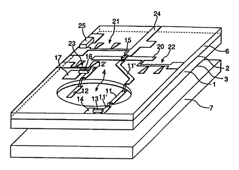
Fig. 1 is a partial perspective view of a VCO module.
In Fig. 1, reference numeral 1 denotes a dielectric sheet.
Electrodes 2 ad 3 are formed on the respective two main
surfaces of the dielectric sheet 1. Each electrode 2, 3 has
an opening formed at a location corresponding to the
location of the opening of the other electrode. In Fig. 1,
reference numeral 4 denotes an opening formed in the
electrode disposed on the upper surface of the dielectric
sheet 1. Reference numeral 6 denotes a circuit board in the
form of a dielectric sheet having an opening formed at a
location corresponding to the electrode opening 4. Various
circuits are formed on the upper surface of the circuit
board 6, as described below. They include a transmission
line 11' connected to a coupling line 11 formed in the
electrode opening 4 and a transmission line 12' connected to
a coupling line 12 formed in the electrode opening 4. A
terminating resistor 13 is provided between one transmission
line 11' and a ground electrode 14. On the other hand, a
varactor diode 16 is disposed between the transmission line
12' and a ground electrode 17. Furthermore, a bias circuit
CA 02262357 1999-02-23
- 13 -
23 is connected to an end of the transmission line 12'.
There is also provided a series feedback line 20, on
which an FET 15 is mounted. Reference numeral 24 denotes an
output circuit. The gate of the FET 15 is connected to an
end of the transmission line 11'. The drain and the source
of the FET 15 are connected to the series feedback line 20
and the output circuit 24, respectively. A bias circuit 22
is connected to the series feedback line 20, and a bias
circuit 21 is connected to the output circuit 24.
Furthermore, a chip resistor 25 is disposed between the end
of the bias circuit 21 and the ground electrode.
Because the back surface of the circuit board 6 is in
contact with the ground electrode formed on the upper
surface of the dielectric sheet 1, microstrip lines are
formed between the respective transmission lines described
above and the ground electrode. Alternatively, a ground
electrode may be formed over the substantially entire area
of the back surface (facing the dielectric sheet 1) of the
circuit board 6.
The coupling lines 11 and 12 are formed on the upper
surface of the dielectric sheet 1, in an area exposed via
the electrode opening. The coupling electrodes 11 and 12
are connected via bonding wires to the electrodes 11' and
12', respectively, formed on the circuit board 6.
Fig. 2 is a cross-sectional view illustrating an
CA 02262357 1999-02-23
- 14 -
electromagnetic field distribution in the dielectric
resonator part. As described above, the electrodes 2 and 3
having circular electrode-openings 4 and 5 formed at
locations corresponding to each other are disposed on both
main surfaces of the dielectric sheet 1 so that the part
defined by the openings 4 and 5 serves as a TE010-mode
dielectric resonator. In the TE010 mode, the intensity of
the electromagnetic field is greater at locations nearer to
the surface of the dielectric sheet 1 in the vicinity of the
electrode openings 4 and 5.
Fig. 3 illustrates an equivalent circuit of the VCO
described above. In this figure, R denotes the dielectric
resonator. The FET 15 forms a negative resistance circuit.
The negative resistance circuit, the coupling line 11, and
the dielectric resonator R coupled with the coupling line 11
form a band reflection oscillator. The oscillation
frequency changes according to the capacitance of the
varactor diode 16 connected to the coupling line 12 coupled
with the dielectric resonator R.
By forming the coupling line directly in the electrode
opening plane in the above-described manner, it is possible
to achieve strong coupling between the dielectric resonator
and the coupling line. Furthermore, in this technique,
because the electrode opening forming the dielectric
resonator and the coupling line are formed on the same
CA 02262357 1999-02-23
- 15 -
single dielectric sheet, it is possible to easily achieve
high positional accuracy between the dielectric resonator
and the coupling line. As a result, it is possible to
easily produce dielectric resonant apparatuses with less
characteristic variations.
Although in the first embodiment, the transmission
lines are formed into the microstrip line structure, they
may also be formed into the coplanar line structure. Fig. 4
illustrates an example in which a coplanar line is employed.
In Fig. 4, of the electrodes formed in the electrode
opening, only a coupling line 11 is shown. In Fig. 4, an
electrode 2 having a circular opening 4 and a coplanar
transmission line including a center conductor 11' are
formed on the upper surface of the dielectric sheet 1. The
center conductor 11' of the coplanar transmission line and
the coupling line 11 are connected to each other via a
bonding wire. When the transmission lines are produced into
the form of coplanar transmission lines in the above-
described manner, the circuit board 6 such as that shown in
Fig. 1 becomes unnecessary at least for the transmission
lines. Because the ground electrode, the transmission lines,
and the coupling lines can all be formed on the dielectric
sheet, the required production process becomes simpler.
Furthermore, high positional accuracy between the dielectric
resonator and the coupling line can be easily achieved.
CA 02262357 1999-02-23
- 16 -
Instead of employing the bonding wire shown in Fig. 4,
the connection may also be achieved using a ribbon wire as
shown in Fig. 5.
Alternatively, as shown in Fig. 6, an interconnecting
member including a conductor 28 may be disposed between the
coupling line 11 and the end of the coplanar transmission
line such that the center conductor 11' of the coplanar
transmission line is connected to the coupling line 11 via
the conductor 28.
Still alternatively, as shown in Fig. 7, the coupling
line 11 may be connected to the center conductor 11' of the
coplanar transmission line via an air bridge 26.
Fig. 8 illustrates an example of a VCO constructed
using transmission lines in the form of coplanar
transmission lines. In Fig. 8, reference numeral 30 denotes
a resonant circuit board including a dielectric sheet 1
wherein electrodes 2 and 3 having openings formed at
locations corresponding to each other are disposed on the
respective two main surfaces of the dielectric sheet 1 so as
to form a TE010-mode dielectric resonator part. Furthermore,
coupling lines 11 and 12 and various transmission lines
including transmission lines 11' and 12' in the form of
coplanar transmission lines are formed on the upper surface
of the dielectric sheet 1. Reference numeral 31 denotes a
negative resistance circuit board. A ground electrode is
CA 02262357 1999-02-23
- 17 -
formed over the substantially entire area of the lower
surface of a dielectric sheet. A negative resistance
circuit including an FET 15 is formed on the upper surface
of the dielectric sheet. This negative resistance circuit
is constructed in a similar fashion to the negative
resistance circuit shown in Fig. 1.
In the resonant circuit board 30, a terminating
resistor 13 is disposed on the upper surface of the
dielectric sheet 1 such that the transmission line 11' is
connected, via the terminating resistor 12, to the electrode
2 serving as the ground electrode. Furthermore, a varactor
diode 16 is disposed between the transmission line 12' and
the ground electrode. The transmission line 12' is also
connected to a bias circuit 23. When both coplanar lines
and microstrip lines are used as is the case in this example,
the resonant circuit board and the negative resistance
circuit board may be produced separately and the
transmission lines on the two board may be connected via a
bonding wire.
Fig. 9 illustrates another example of a VCO
constructed using transmission lines in the form of coplanar
transmission lines. A negative resistance circuit board 31
is similar to that shown in Fig. 8. A resonant circuit
board 30 is different from that shown in Fig. 8 in that
coupling lines 11 and 12 are extended into an outer area
CA 02262357 1999-02-23
- 18 -
from the inside of an electrode opening 4 such that the
extended parts act as coplanar transmission lines. In other
words, the center conductors of the coplanar transmission
lines and the coupling lines are formed of the same
continuous lines. In this structure, the wire bonding for
the connection between the coupling lines and the
transmission lines become unnecessary. As for the
connection between the transmission line on the resonant
circuit board 30 and that on the negative resistance circuit
board 31, the transmission lines may be directly connected
using solder or the like without using a bonding wire.
Fig. 10 is a perspective view illustrating another
example of a vCO constructed using transmission lines in the
form of coplanar transmission lines. In Fig. 10, reference
numeral 26 denotes air bridges extending over center
conductors of coplanar transmission lines extending from the
coupling lines 11 and 12 such that two ground electrodes
(electrodes 2) at both sides of the center conductors are
connected to each other via the air bridges. By disposing
air bridges 26 around the perimeter of the electrode opening
4 such that the resultant structure becomes equivalent to
the structure shown in Fig. 8 in which the electrode opening
is surrounded by a continuous ground conductor, thereby
ensuring that oscillation occurs at an intrinsic resonant
frequency. If the locations of the air bridges 26 are
CA 02262357 1999-02-23
- 19 -
shifted far from the perimeter of the electrode opening 4,
the electromagnetic field distribution near the perimeter of
the electrode opening changes and thus the resonant
frequency changes (decreases). This effect allows the
resonant frequency to be set or adjusted by the locations of
the air bridges 26.
Instead of the air bridges 26 shown in Fig. 10,
bonding wires or ribbon wires may be used to make
connections between the ground electrodes at both sides of
the center conductors of the coplanar transmission lines.
Alternatively, the bridges may be formed using a two-layer
interconnection technique.
Although coplanar transmission lines are employed in
the examples shown in Figs. 8 to 10, the circuit may also be
divided into two modules, that is, a resonant circuit board
30 and a negative resistance circuit board 31, as shown in
Fig. 11 when transmission lines are produced using
microstrip lines. In Fig. 11, a dielectric resonator formed
in resonant circuit electrode openings 4, coupling lines 11
and 12 coupled with the dielectric resonator, and
transmission lines 11' and 12' connected to the respective
coupling lines 11 and 12 are all similar to those shown in
Fig. 1 although there are differences in locations. A
negative resistance circuit board 31 is similar to that
shown in Fig. 8. By dividing the circuit into the resonant
CA 02262357 1999-02-23
- 20 -
circuit module and the negative resistance circuit module as
described above, it becomes possible to separately produce
and adjust those two modules.
Fig. 12 illustrates another technique to connect a
microstrip line formed on a circuit board 6 to a coupling
line formed on a dielectric sheet in an electrode opening.
In this example, the circuit board 6 includes an opening
formed at a location corresponding to the electrode opening
4 formed on the dielectric sheet, and the circuit board 6
partially protrudes into the opening such that the end of
the protruding part reaches an end of the coupling line 11
formed in the electrode opening. The transmission line 11'
in the microstrip line form and the coupling line 11 are
connected to each other at the protruding part via solder or
the like. Instead of using solder, the connection may also
be achieved via capacitance between the transmission line
11' and the coupling line 11.
In the above examples, the coupling lines are simply
formed on the surface of the dielectric sheet 1 in the
electrode opening. Alternatively each coupling line may be
formed into a trench structure as shown in Fig. 13. Such a
trench coupling line may be obtained by forming a trench at
a location where a coupling line is to be formed and then
forming an electrode on the inner surface of the trench. By
employing such an electrode structure, it is possible to
CA 02262357 1999-02-23
- 21 -
reduce the conductor loss and thus increase Qo of the
dielectric resonator.
In the embodiments described above, a circular
electrode opening is formed to realize a TE010-mode
dielectric resonator. Alternatively, a rectangular
electrode opening may be formed so as to realize a
rectangular slot-mode resonator, as shown in Fig. 14. In
this mode, a planar dielectric transmission line acts as a
resonator and thus this mode may be called a PDTL mode.
Fig. 15 illustrates an electromagnetic field
distribution in the PDTL-mode dielectric resonator. By
disposing the coupling line 11 shown in Fig. 14 in a
direction crossing the direction of the magnetic field in
the PDTL mode, it is possible to magnetically couple the
dielectric resonator with the coupling line.