Note: Descriptions are shown in the official language in which they were submitted.
CA 02262~73 1999-02-04
WO 98/06075 PCT/EP97/04116
PA-96/36-PCT-B
Security Element for Electronic Article Surveillance
This invention relates to a security element for electronic
article surveillance, comprising at least one coiled conductive
track and a capacitor having a dielectric layer arranged there-
- between, or comprising two -coiled conductive tracks that are
disposed on either side of a dielectric layer so as to overlap
at least in part (-~ resonant circuit).
Resonant circuits which are excited to resonate at a prede-
termined resonant frequency which is conventionally at 8.2 MHz
are widely accepted to protect articles against pilferage in de-
partment stores. Frequently the circuits are an integral part
of adhesive labels or cardboard tags which are affixed to the
articles to be maintained under surveillance. Typically, the
department store has an electronic surveillance system installed
in the exit area, which detects the resonant circuits and pro-
duces an alarm when a protected article passes through a sur-
veillance zone in unauthorized manner. The resonant circuit is
deactivated when a customer has paid the merch~n~;se. This pre-
vents an alarm being produced once an article has been rightly
acquired by purchase, passing through the surveillance zone sub-
sequently.
The deactivation systems which are frequently installed in
the checkout areas generate a resonant signal of a higher ampli-
tude than it is produced in the surveillance systems. A reso-
nant label is normally deactivated with a field strength greaterthan l.5 A/m. A variety of deactivating mechanisms for resonant
circuits are known in the art. They involve either destroying
the insulation between two opposing conductive tracks, producing
a short circuit, or subjecting a length of conductive track to
overload and causing it to melt, thereby interrupting the cir-
cuit path. In consequence of deactivation, the resonant
CA 02262~73 1999-02-04
WO 98/06075 PCT/EP97/04116
PA-96/36-PCT-B
properties of the resonant circuit, that is, the resonant fre-
quency and/or the "Q" factor are modified so severely that the
resonant label stops being detected by the surveillance system.
There is a risk that the deactivated resonant circuit may
be reactivated inadvertently by mechanical manipulation includ-
ing, for example, folding, packaging and transporting the
merchandise, or bending the label and hence the resonant cir-
cuit. Any accidental reactivation of a resonant circuit which
is affixed to an article rightly acquired by purchase may then
lo produce an alarm leading to embarrassment both for the customer
and for the department store.
So far no state of the art has become known which concerns
itself with the problem of ~;m;n;shing the risk of an accidental
reactivation of resonant labels that are already deactivated.
With regard to the deactivation of resonant labels, different
methods have been described in the art. In U.S. Pat. No.
4,876,555 and its corresponding EP 0 285 559 Bl it is proposed
using a needle to produce a hole in the insulating layer between
two opposite capacitor surfaces. This results in a fault-free
and perm~n~nt deactivation mechanism.
U.S. Pat. No. 5,187,466 describes likewise a method for
generating a deactivatable resonant circuit by means of a short
circuit that cannot be destroyed under normal circumstances.
As regards the first mentioned U.S. Pat. No. 4,876,555 and
its corresponding EP 0 285 559 Bl, it should be noted that the
resonant circuit therein disclosed includes capacitor plates
which are disposed on either side of the dielectric material.
The dielectric layer arranged between the two capacitor plates
has a through hole.
In U.S. Pat. No. 5,187,466 referred to in the foregoing, a
method is described which is applied to a resonant circuit
CA 02262~73 1999-02-04
WO 98/06075 PCT/EP97/04116
PA-96/36-PCT-B
having capacitor plates on either side of the dielectric, and in
which the capacitor plates are first short-circuited and the
short circuit is melted later by the application of electrical
energy.
Still further important techniques in the field of the de-
activation of resonant labels are known which however do not
concern themselves with the reduction of the risk of an acciden-
tal reactivation. A patent family extending in this direction
comprises, among others, EP 0 181 327 Bl, U.S. Pat. No.
I0 4,567,473 and U.S. Pat. No. 4,498,076. The resonant label of
the invention which is described in these patents is composed of
the following components: a substrate material serving as di-
electric, capacitor plates on either side of the planar dielec-
tric substrate material, a deactivation zone and a resonant cir-
cuit which is disposed on the dielectric material. Heretofore
the state of the art has not indicated any provisions that would
prevent an undesirable reactivation after deactivation has taken
place successfully.
It is an object of the present invention to propose a reso-
nant circuit in which the probability of reactivation is
reduced.
This object is accomplished in that provision is made in
the dielectric layer for at least one selected area (a zone of
preferred breaking) in which a short circuit is produced between
the opposed capacitor plates or the coiled conductive tracks by
the supply of energy in sufficiently high amount by an alternat-
ing magnetic field, and in which the selected area is strength-
ened locally such that a destruction of the short circuit (=
conductive path) by mechanical loads, and hence a reactivation
of the security element, are prevented.
- According to an advantageous further aspect of the security
element of the present invention, provision is made for the
CA 02262~73 1999-02-04
WO 98/06075 PCT/EP97/04116
PA-96/36-PCT-s
dielectric layer to be of substantially uniform thickness and to
have no additional manufacturing defects (air inclusions, for
example).
According to a yet further proposal, in the event of two at
least partly overlapplng tracks being used these are wound in
opposite directions, with the seIected area being located at the
outer ends of the tracks. This is the point where the induced
voltage is at its highest level.
In an advantageous aspect of the security element of the
lo present invention, it is proposed making the dielectric layer in
the selected area th; nner than in the remaining areas.
According to an alternative solution, the selected area is
characterized in that the dielectric layer has in this area a
different physical or chemical property than in the r~m~;n;ng
areas.
According to an advantageous further aspect of the security
element of the present invention, the dielectric layer is com-
prised of at least two components. In this connection it is par-
ticularly advantageous for the melting point of the one compo-
nent of the dielectric layer to lie above the productiontemperature for security elements. According to a still further
aspect, the components of the dielectric l-ayer are of a nature
enabling them to be fabricated by either a coating or a laminat-
ing process.
According to an advantageous feature of the security
element of the present invention, the selected area in which the
deactivation takes place is strengthened by the application of
additional pressure. Compression ~nh~nces the bond between the
capacitor plates or the at least partly overlapping tracks. It
has proven to be advantageous to use pressure forming techniques
for strengthening which involves forming the capacitor plates or
CA 02262~73 1999-02-04
WO 98/06075 PCT/EP97/04116
PA-96/36-PCT-B
the at least partly overlapping tracks into a three-dimensional
shape. In this regard it is particularly advantageous if the
enhanced bonding and the forming of the capacitor plates or
tracks are accomplished in a single operation.
When the resonant circuit is bent or folded in the area of
the strong zone, that is the zone where deactivation takes
place, there is still a risk that the resonant circuit may
buckle, shear, slide or delaminate at the point of deactivation.
This would cause undesirable reactivation of the resonant cir-
cuit. In order to forestall this risk, a further aspect of the
present invention involves providing weak zones on either side
of the strong zone. When an external b~ing moment is applied,
the resonant circuit is much more likely to fold or even break
in the area of the weak zones than to fold or break within the
strong zone. The weak zone may therefore be referred to as the
zone of preferred ben~;ng or breaking.
One approach to obtain the weak zones involves narrowing
down the width of the track. Alternatively, the possibility
exists to treat the adhesive layer in these weak zones so that
there is significantly reduced bonding between the coiled
tracks. Alternatively again, the weak zones may be made by per-
forating the tracks.
According to a yet further advantageous aspect of the
present invention, the resonant circuit is configured such that
the capacitance between the upper and lower track is concen-
trated at the inner ends of the coils. In particular, at the
inner ends of the coils the area of track overlap is large, re-
sulting in a proportionally large capacitance, while the area of
overlap at the outer ends of the coils is very small.
In a yet further advantageous aspect of the device of the
present invention, it is proposed that the areas of overlap
between the two tracks and hence the capacitance between the
CA 02262~73 1999-02-04
WO 98/06075 PCT/EP97/04116
PA-96/36-PCT-B
tracks concentrate at the inner ends of the tracks. In particu-
lar, the outer ends of the two tracks overlap in a small area,
and there is a relatively long area with no overlap adjacent to
the outer ends of the tracks. An advantage of this topology is
that it results in deactivation taking place in the area of
o~erlap between the outer ends of the upper and lower tracks as
this is the point of highest voltage potential between the
tracks.
Therefore, there is a high degree of certainty that the
point of deactivation is in the selected area.
The present invention will be explained in more detail in
the following with reference to the accompanying drawings. In
the drawings,
FIG. 1 is a plan view of an embodiment of the resonant
circuit of the present invention;
FIG. 2 is a cross sectional view taken along the line II-II
of FIG. l;
FIG. 3 is an equivalent electrical circuit illustrating the
voltages occurring in two partly overlapping coiled tracks;
FIG. 4 is a plan view of the outer end area of the coiled
tracks;
FIG. 5 is an enlarged cross sectional view of the upper
coil and the upper component of the dielectric layer;
FIG. 6 is a detailed cross-sectional view of the resonant
circuit of the present invention;
FIG. 7 is a plan view of a strong zone;
FIG. 8a is a cross sectional view of a suitable tool;
-- 6
CA 02262~73 1999-02-04
WO 98/06075 PCT/EP97/04116
PA-96/36-PCT-B
FIG. 8b is a plan view of the tool illustrated in FIG. 8a;
FIG. 9 is a plan view of a track with a weak zone;
FIG. 10 is a plan view of a further track with a weak zone;
FIG. lla is a plan view of a configuration of the lower
S coil;
FIG. llb is a plan view of a configuration of the upper
coil;
FIG. llc is a view of the resonant circuit as composed from
the coils shown in FIG. lla and FIG. llb; and
FIG. 12 is an equivalent electrical circuit illustrating
the voltage relationships of the embodiment of the resonant cir-
cuit of the present invention illustrated in FIG. llc.
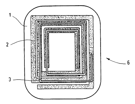
FIG. 1 shows an embodiment of the resonant circuit 6 of the
present invention in plan view. FIG. 2 shows the resonant cir-
cuit 6 of FIG. 1 in cross sectional view. Deactivation of theresonant circuit 6 takes place by producing a short circuit be-
tween the two coiled conductive tracks 2, 3, which are prefera-
bly fabricated from aluminum, through the dielectric layer 4.
The application of an alternating magnetic field as emitted, for
example, by the surveillance system induces alternating voltages
in the two coiled tracks 2, 3 of the resonant circuit 6. The
coiled tracks 2, 3 overlap at least in part and are wound in
opposite directions. Therefore, the outer end of the lower coil
2 has a positive potential with respect to the inner end of the
lower coil 2 when the inner end of the upper coil 3 has a posi-
tive potential with respect to the outer end of the upper coil
3. It will be understood, therefore, that the points/areas in
which the induced alternating voltages between the two coils 2,
3 are at their highest levels are located in the end areas of
the coils 2, 3.
, _
CA 02262~73 1999-02-04
WO 98/06075 PCT/EP97/04116
PA-96/36-PCT-B
Considering that in the example illustrated in FIG. l the
upper coil 3 has fewer turns than the lower coil 2, the highest
voltages are generated between the ends of the upper coil 3 and
the areas of the lower coil 2 situated directly underneath.
s FIG. 3 illustrates clearly the voltage relationships in
different areas of the two at Least partly overlapping coils 2,
3 of a resonant circuit 6 that is suitable for use according to
an advantageous further aspect of the resonant circuit 6 of the
present invention.
In the resonant circuit 6 previously described in which the
dielectric layer 4 between the coils 2, 3 is of uniform thick-
ness, deactivation takes place in the end areas of the upper
coil 3 and the lower coil 2, because this is where the induced
potential is at its highest level. Because the electric field
strength is focused on a surface with a small radius, deactiva-
tion takes place precisely at the ends of the tracks 2, 3, as
shown in FIG. 4.
If however the dielectric layer 4 is not of uniform thick-
ness or contains air inclusions 7 which may happen easily as a
result of manufacturing defects, deactivation may take place in
various areas of the coils 2, 3. Such manufacturing defects may
cause local weaknesses and even produce holes resulting from air
inclusions 7 in the dielectric layer 4. In consequence, the di-
electric layer 4 breaks down at these local weak points although
the voltage potential is lower at these points than it is at the
ends of the upper and lower track 3, 2. Because the voltage po-
tential is lower at the local weak points than it is at the ends
of the tracks 2, 3, the electrical energy available for produc-
ing the deactivation short circuit is smaller than the electri-
cal energy that would be necessary to produce a deactivation
short circuit at the ends of the upper coil 3.
.. ..
CA 02262~73 1999-02-04
WO 98/06075 PCT/EP97/04116
PA-96/36-PCT-B
FIG. 5 shows a cross section of a dielectric layer 4 exhib-
iting manufacturing defects in the form of air inclusions 7 and
irregularities in the surface area. To avoid such manufacturing
defects, the dielectric layer 4 is configured in a further
aspect so that it is substantially uniform in thickness and
la~gely free from local weak points 7. Such a uniform dielec-
tric layer 4 ensures deactivation in the end areas of the coiled
tracks 2, 3 as this is the point of highest induced voltage and
energy. A short circuit produced by such deactivation is very
robust with little susceptibility to accidental reactivation.
According to an advantageous further aspect of the resonant
circuit 6 of the present invention, the dielectric layer 4 is
comprised of at least two components 4a, 4b, including an upper
component 4a and a lower component 4b. The lower component 4b
is applied to the lower coil 3 prior to stamping and hot emboss-
ing. The upper component 4a is applied to the upper coil 2.
The upper component 4a has a relatively low melting point
enabling it to serve as a hot-melt-type adhesive and to adhe-
sively bond the two coils 2, 3 together during hot embossing of
the upper coil 2 onto the lower coil 3. The upper component 4a
of the dielectric layer 4 melts during hot embossing of the
upper coil 2. Having a higher melting point, the lower compo-
nent 4b of the dielectric layer 4 does not melt during hot
embossing on the upper coil 2. The uniformity of the lower com-
ponent 4b of the dielectric layer 4 which does not melt improvesoverall the uniformity of thickness of the dielectric layer 4.
FIG. 6 shows a cross section of a resonant circuit 6 having
a dielectric layer 4 composed of two components 4a, 4b. The
lower component 4b may be produced either by coating the lower
coil 3 or by laminating the lower component 4b of the dielectric
layer 4 onto the coil 3. Typically the coil material (Al) is
available in the form of broad coils enabling the uniformity of
the surface of the dielectric layer 4 to be maintained and other
CA 02262~73 1999-02-04
WO 98/06075 PCT/EP97/04116
PA-96/36-PCT-B
defects caused, for example, by air inclusions 7, to be
minimized.
There is the risk that the short circuit may be broken by
folding or other mechanical manipulations, even when the dielec-
tric layer 4 is so uniform that defects 7 are largely reducedand the deactivation short circuit occurs exclusively at the end
of the upper track where the induced energy is at its highest
level. (This applies of course only in cases where no selected
zone of preferred breaking is provided.) Relative shearing or
sliding motions of the two metal layers or delamination of the
two layers may result in an accidental reactivation.
According to the present invention, the resonant circuit 6
is locally strengthened in the area of the ends of the upper
coil 2 or in the zone of the treated area. The strong zone 10
is less susceptible to shearing and sliding motions or delamina-
tion. By strength~n;ng locally, any stresses, strains or loads
imposed on the resonant circuit 6 by folding or ben~;ng can be
reduced because the two coiled tracks 2, 3 shear, slide, fold or
delaminate only in the proximity of, yet not within, the locally
strengthened zone 10.
According to an advantageous further aspect of the resonant
circuit 6 of the present invention, the zones around the ends of
one of the two tracks 2, 3, here of the upper track 2, are
strengthened by the application of an additional pressure to a
local zone 10, with the metal, which is preferably aluminum,
being formed such as to assume a non-plane shape. Local
pressure application effects an improved bond between the two
tracks 2, 3 and between the lower track 3 and the dielectric
layer 4. When this pressure is applied by means of a forming
tool 11 having a protuberance with a predetermined profile
(punch 12), it is possible to form the tracks 2, 3 so that the
resistance of the resonant circuit 6 to reactivation is
-- 10 --
CA 02262~73 1999-02-04
WO 98/06075 PCT/EP97/04116
PA-96/36-PCT-B
materially improved. It will be understood, of course, that the
tool 11 may also be of a flat configuration and have predeter-
mined dimensions.
With regard to the structural properties of metals it is
well known that a piece of sheet metal having grooves, bulges or
other worked in structures is less susceptible to bending than a
flat piece of sheet metal. The same principle is applied here
to produce a locally strengthened zone 10. Any folding or bend-
ing of the resonant circuit 6 over a large surface area leads to
lo bending, folding, shearing or delaminating of the resonant cir-
cuit 6 in the proximity of, yet not within the strong zone 10.
This reduces the risk of an inadvertent reactivation. The
actual shape of the strong zone 10 is not crucial, nor is the
actual profile of the formed track 2, 3 in the strong zone 10
critical.
FIG. 7 shows an embodiment of a strong 10 at one end of the
upper track 2 in plan view.
FIG. 8a is a cross sectional view, and FIG. 8b a plan view,
of a tool 11 suitable for producing the strong zone 10.
When the resonant circuit 6 is bent or folded in the area
of the strong zone 10, that is the zone where deactivation is
known to take place and which has been deliberately strength-
ened, there is still a risk that the resonant circuit 6 may
buckle, shear, slide or delaminate. This would cause undesir-
able reactivation of the resonant circuit 6. In order to fore-
stall this risk, a further aspect of the present invention in-
volves providing weak zones 13 on either side of the strong zone
10. When an external be~;ng mom~nt is applied, the resonant
circuit 6 is likely to fold or even break in the area of the
weak zones 13. The weak zone 13 may therefore be referred to as
the zone of preferred b~n~;ng or breaking. The weak zone 13 may
be made weak either by narrowing down the width of the track 2,
CA 02262~73 1999-02-04
WO 98t06075 PCT/EP97/04116
PA-96/36-PCT-B
3 as shown in FIG. 9 and FIG. 10, or alternatively by suitably
treating the adhesive layer in this weak zone 13 so that there
is significantly weaker bonding between the tracks 2, 3. A
further possibility to obtain weak zones 13 involves perforating
s the tracks 2, 3.
In a yet further aspect of the present invention, the
tracks 2, 3 and the resonant circuit 6 are configured in such a
way that the capacitance between the upper and lower tracks 2, 3
is concentrated at the inner ends of the coiled tracks 2, 3. A
lo corresponding resonant circuit 6 iS shown in FIG. lla, FIG. llb
and FIG. llc. As becomes apparent from the Figures, at the
inner ends of the coils 2, 3 the area of overlap of the tracks
2, 3 is large, resulting in a proportionally large capacitance,
while at the outer ends of the coils 2, 3 the point of overlap
is very small.
The equivalent circuit of this arrangement is shown in FIG.
12. The voltage difference generated between the two coils 2, 3
at the outer ends of the coils is significantly larger than at
any other point between the coils 2, 3. Studying FIG. llc and
FIG. 12 together it will also be noted that a large part of the
outer turn of the lower track 3 is not overlapped by the upper
track 2 at all. Thus there is no possibility of deactivation
taking place along this section 9 of no overlap. Tracing the
outer turn of the lower track 3 back from the end point where
there is a small area of overlap with the upper track 2, it will
be noted that the next point at which there is overlap of the
tracks 2, 3 and therefore the possibility of deactivation
exists, is further back along the outer turn of the lower track
3. This point has considerably less voltage potential between
the upper and lower tracks 2, 3.
Even if the dielectric layer 4 between the two tracks is
not perfectly uniform in thickness or perfectly free from other
CA 02262~73 1999-02-04
WO 98/06075 PCT/EP97/04116
PA-96/36-PCT-B
weaknesses 7, deactivation will take place at this point of
outer overlap because there is considerably more potential
difference between the tracks 2, 3 at this point.
A further advantage is that because the distribution of
potential difference along the length of the tracks 2, 3 is no
longer even, the amount of energy available to make a deactivat-
ing short circuit between the tracks 2, 3 needs to be higher
than it would be with an even distribution of voltage and
capacitance. Higher energy in turn means a more reliable short
circuit and hence automatically less risk of accidental
reactivation.
- 13 -
CA 02262~73 1999-02-04
WO 98/06075 PCT/EP97/04116
PA-96/36-PCT-B
List of References
1 substrate material
2 upper coil
3 lower coil
4 dielectric layer
4a upper component
4b lower component
adhesive layer
6 resonant circuit or security element
7 air inclusion
8 (treated) selected area
9 area of no overlap
strong zone
11 tool
12 punch
13 weak zone
- 14 -