Note: Descriptions are shown in the official language in which they were submitted.
CA 02262~79 1999-01-2~
WO 98/06541 PCT/US97113047
ABRASIVE CONSTRUCT~ON FOR SEMICONDUCTOR WAFER
MODIFICATION
~ Ba-~k~round of the InventionThis invention relates to an abrasive construction having abrasive, rigid, and
resilient elements for modifying an exposed surface of a semiconductor wafer.
In the course of integrated circuit m~nl~f~ctllre, a semiconductor wafer
typically undergoes numerous processing steps, including deposition, patterning,and etching steps. Additional details on how semiconductor wafers are processed
10 can be found in the article "Abrasive Machining of Silicon" by Tonshoff, H.K.;
SchPiden, W.V.; Tn~c~ki, I.; Koning, W.; Spur, G. published in the Annals of theInternational Institution for Production Engineerin~ Research~ Volume 3912/1990,pages 621 to 63 5. At each step in the process, it is often desirable to achieve a pre-
deterrnined level of surface "planarity" and/or ''uluroll,lily.'' It is also desirable to
1~ ...il~;,..i~e surface defects such as pits and scratches. Such surface irregularities may
affect the performance of a final patterned semiconductor device.
One accepted method of reducing surface irregularities is to treat the wafer
surface with a slurry cont~ining a plurality of loose abrasive particles using apolishing pad. An example of a polishing pad for use with a slurry is described in
U.S. Patent No. 5,287,663 (Pierce et al.). This pad includes a polishing layer, a
rigid layer adj~ce~lt the polishing layer, and a resilient layer ~dj~cPnt the rigid layer.
The polishing layer is material such as urethane or composites of urethane.
Summarv of the Invention
The present invention provides an abrasive construction for modifying a
surface of a workpiece. The abrasive construction comprises: a three-dimensional,
textured, fixed abrasive çlemçnt; at least one resilient element generally coextensive
with the fixed abrasive Plem~nt; and at least one rigid element generally coextensive
with and interposed between the resilient element and the fixed abrasive element,
CA 02262~79 1999-01-2~
WO 98106541 PCT/US97/13047
wherein the rigid element has a Young's Modulus greater than that of the resilient
element. The combination of the rigid and resilient elements with the abrasive
Pl~ment provides an abrasive construction that sub~ lly conforms to the global
topography of the surface of a workpiece while not subst~nti~lly col~folllling to the
local topography of a workpiece surface during surface modification.
Another embodiment of the abrasive construction comprises: a
three-dimensional, textured, fixed abrasive article comprising a baclring on which is
disposed an abrasive coating, and a subpad generally coextensive with the backing
of the fixed abrasive article. The subpad comprises: at least one resilient element
having a Young's Modulus of less than about 100 MPa and a rem~ining stress in
compression of at least about 60%; and at least one rigid element generally
coextensive with and interposed between the resilient element and the backing ofthe fixed abrasive article, wherein the rigid element has a Young's Modulus that is
greater than that of the resilient element and is at least about 100 ~a.
Yet another embodiment of the abrasive construction of the present
invention comprises: a three-dimensional, textured, fixed abrasive article
comprising a backing on which is disposed an abrasive coating; and a subpad. Thesubpad is generally coextensive with the backing of the fixed abrasive article and
comprises: at least one resilient element having a Young's Modulus of less than
about 100 MPa, a ~k~ g stress in compression of at least about 60%, and a
thickness of about 0.5-5 mm; and at least one rigid element generally coextensive
with and interposed between the resilient element and the backing of the fixed
abrasive article, wherein the rigid element has a Young's Modulus that is greater
than that ofthe resilient element and at least about 100 MPa, and has a thi~.~ness of
about 0.075-1.5 mm.
Throughout this application, the following definitions apply:
"Surface modification" refers to wafer surface lre~ ç.~l processes, such as
poli.~hin~ and pl&nd i~ing;
"Rigid element" refers to an el~m~nt which is of higher modulus than the
30 resilient e~ nt and which deforms in flexure;
CA 02262~79 1999-01-2~
WO 9~106541 PCT/US97/13047
"Resilient ~Ic-,-e~l" refers to an ~lPmçnt which supports the rigid element,
el~tir~lly derc "~ g in co~l~prei";on;
"Modulus" refers to the elastic modulus or Young's Modulus of a material;
for a resilient material it is measured using a dynamic compressive test in the
thic~ness direction of the material, whereas for a rigid material it is measured using
a static tension test in the plane of the material;
"Fixed abrasive element" refers to an integral abrasive Plem~nt, such as an
abrasive article, that is substanti~lly free of l.n~tt~ched abrasive particles except as
may be generated during modification of the surface of the workpiece (e.g.,
planarization);
"Three-dimensional" when used to describe a fixed abrasive cle.,.~ refers
to a fixed abrasive element, particularly a fixed abrasive article, having numerous
abrasive particles e~tçntlin~ throughout at least a portion of its thickness such that
removing some of the particles at the surface during planarization exposes
additional abrasive particles capable of pe~ro-l.,ing the planarization function;
"Textured" when used to describe a fixed abrasive elemPnt refers to a fixed
abrasive e~mcnt, particularly a fixed abrasive article, having raised portions and
- recessed portions in which at least the raised portions contain abrasive particles and
binder;
"Abrasive composite" refers to one of a plurality of shaped bodies which
collectively provide a textured, three-dim~n~ional abrasive element coml)-;sillgabrasive particles and binder; the abrasive particles may be in the form of abrasive
agglomerates; and
"Precisely shaped abrasive composite" refers to an abrasive composite
having a molded shape that is the inverse of the mold cavity which is retained after
the composite has been removed from the mold; preferably, the composite is
subst~nti~lly free of abrasive particles protruding beyond the exposed surfaces of
the shape before the abrasive article has been used, as described in U.S. Patent No.
5,152,917 (Pieper et al.).
~ 30
CA 02262~79 1999-01-2~
WO 98/06541 PCT/US97/13047
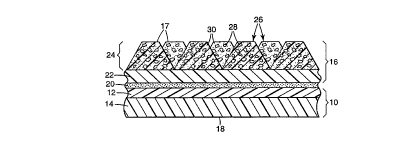
Brief De~ ,lion of the D. ,.~. i..~
Figure 1 is a cross-sectional view of a portion of the subpad of the present
invention attached to a three-dimensional, textured, fixed abrasive element.
S Detailed D~s~ Lion of Invention
The present invention provides an abrasive construction for modifying an
exposed surface of a workpiece such as a semiconductor wafer. The abrasive
construction inc.l~ldes a three-dimensional, textured, fixed abrasive element, aresilient element, and a rigid ~l~ment interposed be~weell the resilient elem~nt and
the fixed abrasive element. These elements are subst~nti~lly coextensive with each
other. The fixed abrasive element is l~eÇ~.ably a fixed abrasive article. Suitable
three-dimensional, textured, fixed abrasive articles, typically comprising a backing
on which is disposed an abrasive coating that includes a plurality of abrasive
particles and a binder in the form of a pre-determined pattern, and methods for
using them in semiconductor wafer processing are disclosed in U. S . Patent
Application Serial No. 081694,014, filed on August 8.
The abrasive constructions of the present invention include at least one
relatively high modulus rigid element and at least one lower modulus resilient
el~mPnt Typically, the modulus of the resilient element (i.e., Young's Modulus in
the thicl~ness direction of the material) is at least about 25% (preferab}y at least
about 50%) less than the modulus of the rigid element (i.e., Young's Modulus in the
plane of the material). Preferably, the rigid element has a Young's Modulus of at
least about 100 MPa, and the resilient element has a Young's Modulus of less than
about 100 MPa. More p~ ably, the Young's Modulus of the resilient element is
less than about 50 MPa.
The rigid and resilient elements provide a subpad for the abrasive Pi~.m~.nt
As shown in Figure 1, subpad 10 in~ des at least one rigid element 12 and at least
one resilient ~l~m~nt 14, which is attac.hed to a fixed abrasive article 16. The rigid
elem~nt 12 is interposed between the resilient element 14 and the fixed abrasivearticle 16, which has surfaces 17 that contact a workpiece. Thus, in the abrasive
constructions ofthe present invention, the rigid element 12 and the resilient rle."~
--4-
CA 02262~79 1999-01-2~
WO 98/06541 PCT/US97/13047
14 are generally cocontinuous with, and parallel to, the fixed abrasive article 16,
such that the three elements are substantially coextensive. Although not shown in
Figure 1, surface 18 ofthe resilient el~m~nt 14 is typically attached to a platen of a
machine for semiconductor wafer modification, and surfaces 17 of the fixed
abrasive article contacts the semiconductor wafer.
As shown in Figure 1, this embodiment of the fixed abrasive article 16
incl~ldes a backing 22 having a surface to which is bonded an abrasive coating 24,
which inc1~ld~s a pre-determined pattern of a plurality of precisely shaped abrasive
composites 26 comprising abrasive particles 28 dispersed in a binder 30. Abrasive
coating 24 may be continuous or discontinous on the backing. In certain
embodiments however, the fixed abrasive article does not require a backing.
~urtherrnore, the rigid element of the abrasive construction could be provided by
the backing of the fixed abrasive article, at least in part.
Although Figure 1 displays a textured, three-dimensional, fixed abrasive
elçmçnt having precisely shaped abrasive composites, the abrasive compositions of
the present invention are not limited to precisely shaped composites. That is, other
textured, three-dimensional, fixed abrasive elements are possible, such as thosedisclosed in U.S. Patent Application Serial No. 08/694,014, filed on August 8,
1996.
There may be intervening layers of adhesive or other att~hmçnt means
between the various components of the abrasive construction. For example, as
shown in Figure 1, adhesive layer 20 is interposed between the rigid elçment 12 and
the bacl~ing 22 of the fixed abrasive article 16. ~lthough not shown in Figure 1,
there may also be an adhesive layer interposed between the rigid element 12 and the
resilient elçm~n~ 14, and on the surface 18 ofthe resilient element 14.
During use, the surfaces 17 of the fixed abrasive article 16 contact the
workpiece, e.g., a semiconductor wafer, to modify the surface of the workpiece to
achieve a surface that is more planar and/or more uniform and/or less rough thanthe surface prior to lle~ The underlying co..ll~inalion of the rigid and resilient
~ 30 ~lem~nt.~ of the subpad provides an abrasive construction that subst~nti~lly
conrol..~s to the global topography of the surface of the workpiece (e.g., the overall
-5 -
CA 02262~79 1999-01-2~
WO 98/06541 PCT/US97113047
surface of a semiconductor wafer) while not subst~l-ti~lly conl~rll,ing to the local
topography of the surface of the workpiece (e.g., the spacing between ~ cent
f~aLules on the surface of a semiconductor wafer) during surface modification. As a
result, the abrasive construction of the present invention will modify the surface of
5 the workpiece in order to achieve the desired level of planarity, ulfirolll,ily, and/or
ro~1~hness. The particular degree of planarity, unirollniLy, and/or rol1~hn~c.c desired
will vary depending upon the individual wafer and the application for which it is
intenderl, as well as the nature of any subsequent proces~in~ steps to which thewafer may be subjected.
Although the abrasive constructions of the present invention are particularly
suitable for use with processed semicondllc.tor wafers (i.e., patterned semiconductor
wafers with circuitry thereon, or blanket, nonpatterned wafers), they can be used
with unprocessed or blank (e.g., silicon) wafers as well. Thus, the abrasive
constructions of the present invention can be used to polish or planarize a
15 semiconductor wafer.
The primary purpose of the resilient element is to allow the abrasive
construction to subst~nti~lly co~ . to the global topography of the surface of the
workpiece while I~AintAil-ing a uniforrn pressule on the workpiece. For exarnple, a
semiconductor wafer may have an overall shape with relatively large und~ tions or
20 variations in thickness, which the abrasive construction should substantially match.
It is desirable to provide substantial conformance of the abrasive construction to the
global topography of the workpiece so as to achieve the desired level of U~ o~",ily
after modification of the workpiece surface. ~ecause the resilient element
undergoes colnp~is~;on during a surface modification process, its resiliency when
25 compressPd in the l~ L~p~ss direction is an i,.lpo,la"l characteristic for achieving
this purpose. The resiliency (i.e., the stiffness in compres~ion and elastic rebound)
of the resilient el~m~nt is related to the modulus of the material in the thickness
di, ~clion, and is also affected by its thickness.
The primary purpose of the rigid element is to limit the ability of the
30 abrasive construction to ~Ub~ lly COl~llll to the local features of the surface of
the wolklJiece. For example, a semiconductor wafer typically has adjacent features
-6-
CA 02262~79 l999-0l-2~
WO 98/06541 PCT/USg7/13047
of the same or dirreren~ heights with valleys between, the topography to which the
abrasive construction should not substantially conform. It is desirable to ~tten~l~te
co,~,l.,ance of the abrasive construction to the local topography of the workpiece
so as to achieve the desired level of planarity of the wolk~;ece (e.g., avoid dishing).
5 The bel~dh~g stiffnPsc (i.e., rçsict~nce to deformation by bending) of the rigid
element is an i"-po-lanl characteristic for achieving this purpose. .The bendingstiffness of the rigid element is directly related to the in-plane modulus of the
material and is affected by its thickness. For example, for a homogeneous material,
the bending ~ .P.s.c is directly proportional to its Young's Modulus times the
10 thiçl~ne-ss ofthe material raised to the third power.
The rigid and resilient elements of the abrasive constructions are typically
separate layers of di~lGnl materials. Each portion is typically one layer of a
material; however, each ~lPm~nt can include more than one layer of the same or
di~e~.~ materials provided that the mechanical behavior of the layered element is
15 acceptable for the desired application. For example, a rigid PlennPnt can include
layers of rigid and resilient materials arranged so as to give the required bending
stiffnçss Similarly, a resilient Plçment can include layers of resilient and rigid
materials as long as the overall l~min~te has sl-fficient resiliency.
It is also envisioned that the rigid and resilient elements can be made from
20 materials having a gradation of modulus. For example, the role of the resilient
element could be played by a foam with a gradient in the pore structure or crosslink
density that provides lessPning levels of rigidity throughout the thickness of the
foam. Another ~Y~mrle is a sheet of rigid material that has a gradient of fillerthroughout its th~ ness to vary its s~ es~ Finally, a material desi~ned to have a
25 gradient in modnlllc throughout its thicl~n~$c could be used to effectively perform
the roles of both the rigid and the resilient elem~nt~ In this way, the rigid and
resilient elements are integral within one layer of material.
The materials for use in the rigid and resilient elem~ntC are pler~ bly
selected such that the abrasive construction provides ul~iroJIll material removal
30 across the WOI~ ) ece surface (i.e., uniformity), and good planarity on patterned
wafers, which includes flatness (measured in terms of the Total Indic?ted Runout
-7-
CA 02262~79 1999-01-2~
WO 98/06~41 PCT/US97113047
(TIR)), and dishing (measured in terms of the planarization ratio). The particular
planarity values depend on the individual wafer and the application for which it is
intended. as well as the nature of subsequent proce~sing steps to which the wafer
may be subjected.
S The flatness quantity TIR is a well known term in the semiconductor wafer
industry. It is a measure of the flatness of the wafer in a specified region of the
wafer. The TIR value is typically measured along a line in a specified area of the
semiconductor wafer using an instrument such as a TENCOR P-2 Long Scan
Profilometer, available from Tencor of Mountain View, CA. It is the dict~nce
between two im~gin~ry parallel planes, one that intersects or touches the highest
point of the surface of a semiconductor wafer and the other that intersects or
tollc.hes the lowest point of the surface of the semiconductor wafer in the area of
consideration. Prior to plana~ lion, this distance (average of ten TIR readings) is
typically greater than about 0.5 mm, sometimes greater than about 0.8 mm or evengreater than about 1-2 mm. As a result of planarization, it is ple~ d that this
distance be less than about 5000 Angstroms, preferably no more than about 1500
~ IIIS.
As is well-known in the art, the amount of dishing is in.1ic~ted by the
planarization ratio, which co~llpares the amount of material removed from the high
regions, which are typically the desired regions of removal, to the amount of
material removed from the low regions, where removal is typically not desired.
Two instruments are used to measure the planalizalion ratio. A profilometer is
used to measure TIR before and after planarization. An optical
intelrt;lellce/absorption instrument is used to measure the thickness of the oxide
layer in areas b~;lween metal il"~rcom~ecls, for example, before and after
planarization. The amount of material removed from each area is determined and
the planali~.alion ratio c~lc~ ted The planarization ratio is the ratio of the amount
of material removed from the high regions (typically the desired regions of removal)
plus the amount of the material removed from the low regions (typically the regions
where removal is not desired) divided by the amount of material removed from thehigh regions. In general, this planarization ratio should be less than 2. A
--8-
CA 02262~79 1999-01-2~
WO 98/06541 PCT/US97/13047
planarization ratio of 1 is typically p~ere"ed because this indicates that there is
effectively no dishing.
Ul~-ro.l"~ly of material removal across a workpiece surface, which is often
reported along with removal or cut rate, is calculated by the following formula:
- % ul.lfo~ ily = [(si2 + sf2)~'/(hi - hf)] x 100
wherein: sj is the standard deviation of the initial material thickness; Sf iS the
standard deviation of the final material thickness; hi is the initial material thic~ness;
10 hf is the final material thickness. Ul~ro~ ies are preferably less than about 15%,
more preferably less than about 10%, and most preferably less than about 5%.
The average cut rate depends upon the composition and topography of the
particular wafer surface being treated with the abrasive construction. In the case of
metal oxide-co.~ surfaces (e.g., silicon dioxide-cont~ining surfaces), the cut
15 rate should typically be at least about 100 Angstroms/minute, preferably at least
about 500 Angstroms/minute, more preferably at least about 1000
Angstroms/minute, and most preferably at least about lS00 Angstroms/minute. In
some in~t~nççc it may be desirable for this cut rate to be as high as at least about
2000 Angstroms/minute, and even 3000 or 4000 Angstroms/minute. While it is
20 generally desirable to have a high cut rate, the cut rate is selected such that it does
not co"-p~u~nlse the desired topography of the wafer surface.
The choice of materials for the rigid and resilient elements will vary
depending on the compositions of the workpiece surface and fixed abrasive element,
the shape and initial flatness of the workpiece surface, the type of appa,~ s used
25 for modifying the surface (e.g., planarizing the surface), the press~l~es used in the
modificatiûn process, etc. As long as there is at least one rigid element and at least
one resilient element~ with at least one rigid element subst~nti~lly coextensive with
and interposed between the fixed abrasive element and the resilient element, theabrasive construction of the present invention can be used for a wide variety of30 semiconductor wafer modification applications.
The materials suitable for use in the subpad can be characterized using
dar~ test methods proposed by ASTM, for example. Static tension testing of
g
CA 02262S79 1999-01-2S
wo 98/06541 Pcr/uss7/13047
rigid materials can be used to measure the Young's Modulus (often referred to asthe elastic mo~ lu~) in the plane of the material. For measuring the Young's
Modulus of a metal, ASTM E345-93 (Standard Test Methods of Tension Testing
of Metallic Foil) can be used. For measuring the Young's Modulus of an organic
5 polymer (e.g., plastics or reil~olced plastics), ASTM D638-84 (Standard Test
Methods for Tensile Plopc,lies of Plastics) and ASTM D882-88 (Standard Tensile
Flopc~ Iies of Thin Plastic Sheet) can be used. For l~minstted e~ .e~ that include
multiple layers of materials, the Young's Modulus of the overall element (i.e., the
Iztmin~te modulus) can be measured using the test for the highest modulus material.
10 Preferably, rigid materials (or the overall rigid element itself) have a Young's
Modulus value of at least about 100 MPa. Herein, the Young's Modulus of the
rigid element is determined by the apprup,iate ASTM test in the plane defined bythe two major surfaces of the material at room temperature (20-25~C).
Dynamic cor"plessi~re testing of resilient materials can be used to measure
15 the Young's Modulus (often referred to as the storage or elastic modulus) in the
thickness direction of the material. Herein, for resilient materials ASTM D5024-94
(Standard Test Methods for Measuring the Dynamic Mechanical Properties of
Plastics in Compression) is used, whether the resilient elçm~nt is one layer or a
lztmirtstted ele.m~nt that in~ des multiple layers of materials. Plcrel~ly, resilient
20 materials (or the overall resilient ele.llel-~ itself) have a Young's Modulus value of
less than about 100 MPa, and more plcft;l~bly less than about 50 MPa. Herein, the
Young's Modulus of the resilient element is determined by ASTM D5024-94 in the
thickness direction of the materia} at 20~C and 0.1 Hz with a preload of 34.5 kPa.
Suitable resilient materials can also be chosen by additionally ev~ ting
25 their stress relaxation. Stress relaxation is evaluated by deforming a material and
holding it in the deformed state while the force or stress needed to mztintztin
d~ro,.,laIion is measured. Suitable resilient materials (or the overall resilient
el~.m~nt) prefelably retain at least about 60% (more preferably at least about 70%)
ofthe initially applied stress a~er 120 seconds. This is ,ere"ed to herein, int~.lurling
30 the claims, as the "te... t;t~ g stress" and is determined by first co",pres~ing a
sample of material no less than 0.5 mm thick at a rate of 25.4 mm/minute until an
-10-
, . . .
CA 02262S79 1999-01-2S
WO 98/06541 PCT/US97113047
initial stress of 83 kPa is achieved at room telllpel~ re (20-25~C), and measuring
the rPn~ining stress after 2 minlltes
The rigid and resilient elem~nts of the abrasive constructions can be of a
variety of thirl~neesec, depending on the Young's ~odulus of the material. The
S thickness of each portion is chosen such that the desired planarity, ul~iro~miLy, and
rou~hness are a~'~ie~ed. For example, a suitable thickness for a rigid elemçnt with a
modulus of 100 MPa is about 1.5 mm. Typically, however, the rigid ~lem~nt can beabout 0.075-1.5 mm thick, depen~1ing on its modulus. Typically, as the Young's
Modulus for a material incl~,ases, the required thirl~ness of the material decreases.
10 A suitable thickness for a resilient element with a modulus of less than about 100
MPa is typically about 0.5-5 mm preferably about 1.25-3 mm.
The rigid elemP-nt is typically selected such that the abrasive construction is
capable of not substantially conforming to the workpiece surface local topography
over a gap width between features of at least about 1.2 mm, preferably at least
15 about 1.5 mm, more preferably at least about 1.7 mm, and most prererably at least
about 2.0 mm, when subjected to an applied pressure of about 80 kPa. This means
that with gap widths smaller than the specified value, there ~,vill be no substantial
conformance to local topography at this particular pressure. Generally, higher and
lower pressures can be used without subslal,lial conrollllallce, as for example, the
20 pressures typically experienced in wafer planarization. A si~nific~nt advantage of
the present invention is the ability to bridge larger gap widths, which is typically
more difflcult to achieve.
Rigid materials for use in the abrasive constructions can be selected from a
wide variety of materials, such as organic polymers, inorganic polymers, ceramics,
25 metals, composites of organic polymers, and combinations thereof. Suitable
organic polymers can be thermoplastic or thermoset. Suitable thermoplastic
materials in~ de~ but are not limited to, polycarbonates, polyesters, polyurethAnes,
polystyrenes, polyolefins, polyperfluoroolefins, polyvinyl chlorides, and copolymers
thereo~ Suitable thermosetting polymers in~lude, but are not limited to, epoxies,
30 polyimides, polyesters, and copolymers thereof. As used herein, copolymers
CA 02262~79 1999-01-2~
WO 98/06541 PCT/US97/13W7
include polymers cot-lA;~ g two or more di~rel.l monomers (e.g., terpolymers,
tetrapolymers, etc.).
The organic polymers may or may not be lei"ro.ced. The rei~rorce.l.el.l can
be in the form of fibers or particulate material. Suitable materials for use as
5 . t;inrol ce..~enl in~ d~ but are not limited to, organic or inorganic fibers (continuous
or staple~, silicates such as mica or talc, silica-based materials such as sand and
quartz, metal par~ic~ t~ glass, metAllic oxides, and calci~lm carbonate.
Metal sheets can also be used as the rigid element. Typically, because
metals have a relatively high Young's Modulus (e.g., greater than about 50 GPa),very thin sheets are used (typically about 0.075-0.25 mm). Suitable metals include,
but are not limited to, ~l~lminllm, stainless steel, and copper.
Specific materials that are useful in the abrasive constructions of the present
invention inçhlde, but are not limited to, poly(ethylene terephthAl~te),
polycarbonate, glass fiber le"~orced epoxy boards ~e.g., FR4, available from
Minnesota Plastics, Minneapolis, MN), Alumim-m, stainless steel, and IClO00
(available from Rodel, Inc., Newark, DE).
Resilient materials for use in the abrasive constructions can be selected from
a wide variety of materials. Typically, the resilient material is an organic polymer,
which can be thermoplastic or thermoset and may or may not be inherently
elastomeric. The materials generally found to be useful resilient materials are
organic polymers that are foamed or blown to produce porous organic structures,
which are typically referred to as foams. Such foams may be prepaled from natural
or synthetic rubber or other thermoplastic elastomers such as polyolefins,
polyesters, polyamides, polyule1l-Anes, and copolymers thereof, for example.
2~ Suitable synthetic thermoplastic elastomers inchlde7 but are not limited to,chlo,uprele rubbers, ethylene/propylene rubbers, butyl rubbers, polybutadienes,
polyisoprenes, EPDM polymers, polyvinyl chlorides, polychlor~p, t;nes, or
~lyl~n~/butadiene copolymers. A particular example of a useful resilient material is
a copolymer of polyethylene and ethyl vinyl acetate in the form of a foam.
~ 30 Resilient materials may also be of other constructions if the app~ul~liale
meçh~nical plope~ies (e.g., Young's Modulus and lC:lllA;llin~ stress in compression)
-12-
.... ~ ~ .. ..
CA 02262~79 1999-01-2~
WO 98106541 PCT/US97/~3047
are attained. Polyurethane i.,.,~e~.~ated felt-based materials such as are used in
conventional polishing pads can be used, for example. The resilient material mayalso be a nonwoven or woven fiber mat of, for example, polyolefin, polyester, orpolyamide fibers, which has been h..~.~..~tecl by a resin (e.g. polyllr~tllane). The
5 fibers may be of finite length (i.e., staple) or subst~nti~lly continuous in the fiber
mat.
Specific resilient materials that are useful in the abrasive constructions of the
present invention in~ de, but are not limited to, poly(ethylene-co-vinyl acetate)
foams available under the trade deci~n~tions CELLFLEX 1200, CELLFLEX 1800,
CELLFI,EX 2200, CELLFLEX 2200 XF (Dertex Corp., Lawrence, MA), 3M
SCOTCH brand CUSHION-MOUNT Plate Mounting Tape 949 (a double-coated
high density elastomeric foam tape available from 3M Company, St. Paul, MN),
EMR 1025 polyethylene foam (available from Sentinel Products, Hyannis, NJ),
HD200 polyurethane foam (available from Illbruck, Inc., Minneapolis, M:N),
MC8000 and MC8000EVA foams (available from Sentinel Products), SUBA IV
Il.,prc~ ed Nonwoven (available from Rodel, Inc., Newark, DE).
Suprisingly, it has been discovered that commercially available pads, or
portions thereof, which have both rigid and resilient el~m~nt~ used in slurry
polishing operations may also be useful as the subpads of the present invention.This discovery is surprising in that the slurry pads are designed to convey loose
abrasive particles to the wafer surface and would not have been expected to
function as an effective subpad for a fixed abrasive el~m~nt Examples of such pads
include those available under the trade design~tions IC1400, IC2000, or IC1000-
SUBA IV pad stacks (available from Rodel, Inc., Newark, DE).
The abrasive constructions of the present invention can further include
means of ~tt~hm~nt between the various components, such as between the rigid
and resilient e~ P ~S and between the rigid ele.ment and the abrasive elçrn~nt For
~Y~mple, the construction shown in Figure 1 is p~epared by l~ e a sheet of
rigid material to a sheet of resilient material. ~ ~min~tion of these two elements can
be achieved by any of a variety of commonly known bonding methods, such as hot
melt adhesive, pressure sensitive adhesive, glue, tie layers, bonding agents,
-13-
CA 02262~79 1999-01-2~
WO 98/06541 PCT/US97113047
mech~nical f~.~te.li~ devices, ultrasonic welding, thermal bonding, microwave-
activated bonding, or the like. Alternatively, the rigid portion and the resilient
portion of the subpad could be brought together by coextrusion.
Typically, l~min~tion of the rigid and resilient el~ment~ is readily achieved byuse of an adhesive, of the pressure sensitive or hot melt type. Suitable pressure
sensitive adhesives can be a wide variety of the conlll,ollly used pressure sensitive
adhesives, inclu-~ing, but not limited to, those based on natural rubber,
(meth)acry}ate polymers and copolymers, AB or ABA block copolymers of
thermoplastic rubbers such as styrene/but~diçne or styrene/isoprene block
copolymers available under the trade design~tion KRATON (Shell Chemical Co.,
Houston, TX), or polyolefins. Suitable hot melt adhesives incl~ldç, but are not
limited to, a wide variety of the commonly used hot melt adhesives, such as those
based on polyester, ethylene vinyl acetate (EVA), polyamides, epoxies, and the like.
The principle requi~e~el~ls of the adhesive are that it has sufficient cohesive
strength and peel resict~nce for the rigid and resilient elements to remain in place
during use, that it is les,sla~l to shear under the conditions of use, and that it is
res;s~ant to chemical degradation under conditions of use.
The fixed abrasive element can be ~tt~ched to the rigid portion of the
construction by the same means outlirled immç~ tely above -- adhesives,
coextrusion, thermal bonding, mechanical f~ctening devices, etc. However, it need
not be attached to the rigid portion of the construction, but l~ e~l in a position
;""~lçdi,~ely ~ cçnt to it and coeAIens;~e with it. In this case some mechanicalmeans of holding the fixed abrasive in place during use will be required, such as
pl~cement pins, .el~;l.;ng ring, tension, vacuum, etc.
The abrasive construction described here is placed onto a m~chine platen for
use in modifying the surface of a silicon wafer, for example. It may be attached by
an adhesive or mech~nical means, such as placement pins, ret~ining ring, tension,
vacuum, etc.
The abrasive constructions of the present invention can be used on many
types of m~f.hines for plana,-~,,n~, semiconductor wafers, as are well known in the
art for use with poiishing pads and loose abrasive slurries. An example of a suitable
-14-
, . . . .... ...
CA 02262S79 1999-01-2S
WO 98106S41 PCT/US97/13047
commercially available m~çlline is a Chemical Mechanical Plana,i~ion (CMP)
m~r.lline available from IPEC/WESTECH of Phoenix, AZ.
Typically, such m~chine~ include a head unit with a wafer holder, which may
consist of both a ret~ining ring and a wafer support pad for holding the
5 semiconductor wafer. Typically, both the semiconductor wafer and the abrasive
construction rotate, preferably in the same direction. The wafer holder rotates
either in a circular fashion, spiral fashion, elliptical f~hion a nonuniform manner, or
a random motion fashion. The speed at which the wafer holder rotates will dependon the particular apparat-ls, planarization conditions, abrasive article, and the
10 desired planali~lion criteria. In general, however, the wafer holder rotates at a rate
of about 2-1000 revolutions per minute (rpm).
The abrasive construction of the present invention will typically have a
~i~meter of about 10-200 cm, preferably about 20-150 cm, more preferably about
25-100 cm. It may rotate as well, typically at a rate of about 5-10,000 rpm,
preferably at a rate of about 10-1000 rpm, and more preferably about 10-250 rpm.Surface modification procedures which utilize the abrasive constructions of
the present inventions typically involve pressures of about 6.9-138 kPa.
Various mor1ifieatiQns and alterations of this invention will become apparent
to those skilled in the art without departing from the scope and spirit of this
20 invention, and it should be understood that this invention is not to be unduly limited
to the illustrative embodiments set forth herein.
E~am~les
Test Procedures
25 Young's Modulus (Tensile Modulus) - Test A
The Young's Moduli of the rigid plastic component materials used in the
present invention were determined using a static tension test according to ASTM
D638-84 (Standard Test Methods for Tensile Properties of Plastics) and
ASTMD-882-88 (Standard Tensile P~opellies of Thin Plastic Sheeting). The
30 Young's Modulus of metals was deterrnined subst~nti~lly according to ASTM
CA 02262~79 1999-01-2~
WO 98106541 PCT/US97/13047
E345-93 (Standard Test Methods of Tension Testing of Metallic Foil) except that
the gage length was 10.2 cm instead ofthe specfied 12.7 cm.
Dynamic Compression - Test B
The Young's Moduli of the resilient component materials used in the
present invention were deterrnined by dynamic me~ nical testing subst~nti~lly
according to ASTM D 5024-94 (Standard Test Method for Measuring the Dynamic
Mechanical Plopellies of Plastics In Compres~ion). The instrument used was a
~heometrics Solids Analyzer (RSA) made by Rheol~,eL,ics, Inc., Piscataway, NJ. Anominal mean compressive stress of 34.5 kPa was applied to the specimen, then
small cyclic loads were superimposed on the static load to determine the dynamicresponse. Isothermal frequency sweeps were run at 20~C and 40~C, sweeping
between 0.015 Hz and 15 Hz.
Con,pl essi~/e Stress Relaxation Test - Test C
Stress relaxation measurements were determined according to ASTM
E 328-86 ~Method for Stress Relaxation Tests for Materials or Structures).
Circular test sa",ples (20.32 mm in ~ o.ter) were placed between two 25.4 mrn
meter flat plates as specified in ASTM E 328-86, and the plates preloaded with
25 grams to assure that the upper plate contacted the sample. The upper plate was
then rli.cpl~ce(l toward the fixed lower plate at a rate of 25.4 mm/minute until the
load on the sample increased to 2730 grams. On reaching the specified load the
~lisp!~c.o-m~n~ of the upper plate was stopped and the relaxation of the stress of the
sample recorded during the subsequent 120 seconds.
Materials
The following materials were used in the examples below.
CA 02262579 1999-01-25
WO 98/06541 Pcrluss7ll3o47
Table 1
Rigid Components
Tl ~r~c of
Sample E(MPa)
Material Supplier Tested (mm)Test A
Polycarbonate Minnesota
Plastics
Minneapolis,
MN or
Cadill~cPlastics Minne~rolis 0.51
Minneapolis, MN
MN
Reinforced Minnesota 0.51 16,000
Epoxy FR4 Plastics
Minneapolis,
MN
rnin~lm All Foils, Inc. N.S. 72,000
Brooklyn
Heights, OH
IC1000 Rodel,Inc. 1.26 315
Newark, DE
302 Stainless Teledyne N.S. 193,000
Steel Rodney
Earth City, MO
*Literature Value
N.S. = not specified
-17-
CA 02262579 1999-01-25
WO 98106541 PCTIUS97/13047
Table 2
Resilient Compone,lls
E' (MPa)
T} ' ~ ~
of Sample 0.1Hztl0 % Stress
Tested H~ Remaining
Materi~l Description .~ ~p! u- (mm) Test B Test C
CELLFLEX Poly(ethylene co- Dertex 3.602.3/3.4 74.52
1200 vinyl acetate) foam Corporation
Lawrence, MA
CELLFLEX " " 3.605.0/6.0 80.40
1~00
CELLFLEX " " 3.68 8.0/12 87.10
2200 XF
HD200 Polyurethane foam Illbnqck, Inc. 2.30 1.814.5 83.74
Minneapolis,
MN
SUBA IV I~ ,ndted Rodel, Inc., 1.323.9/6.4 70.55
No..~.~)v~-. Newark, DE
Adhesives useful in prepa.;llg the abrasive constructions of the present
invention include 442 PC (available as SCOTCH brand Double Coated Tape), 9482
PC (available as SCOTCH brand Adhesive Transfer Tape), and 7961 PC (available
as SCOTCH brand Double Coated Membrane Switch Spacer). All of the above
adhesives are available from 3M Company, St. Paul, MN.
ExamPle 1
A polypropylene production tool was made by casting polypropylene resin
on a metal master tool having a casting surface comprised of a collection of
~.ljacto.nt trlmr~ted 4-sided pyramids. The res.-lting production tool containedcavities that were in the shape of truncated pyramids. The height of each trlmc~ted
pyramid was about 80 mm, the base was about 178 mm per side and the top was
about 51 mm per side. The cavities were arrayed in a square planar arrangement
with a spacin~ of about 50 cavities per c~ eler
The poly~ropylene production tool was unwound from a winder and an
abrasive slurry (described below) was coated at room temperature into the cavities
-18-
. , ~, . .
CA 02262~79 1999-01-2~
WO 98/06541 PCTIUS97/13047
of the production tool using a vacuum slot die coater. A 76 mm thick poly(ethylene
terephth~l~te) film backing (PPF) primed on one face with an ethylene/acrylic acid
copolymer was brought into contact with the abrasive slurrry coated production
tool such that the abrasive slurly wetted the primed surface of the b~c~ing The
5 abrasive slurry was cured by tr~n.cmittin~ ultraviolet light through the PPF b~L ing
into the abrasive slurry. Two dirrer~..l ultraviolet lamps were used in series to
effect the cure. The first W lamp was a Fusion System ultraviolet light fitted with
a "V" bulb and operated at 236.2 Wattsfcm. The second was an ATEK ultraviolet
lamp equipped with a medillm pressure mercury bulb and operated at 157.5 Watts
10 cm. The production tool was removed from the cured abrasive compositelbacking.
This process was a continuous process that operated at between about 3.0-7.6
meters/minute.
The abrasive slurry consisted of trimethanolpropane triacrylate (10 parts,
TMPTA, available from Sartomer Co., Inc., Exton, PA under the designation
"Sartomer 351"), ll~Y~nerliol diacrylate (30 parts, HDDA, available from Sartomer
Co., Inc. under the design~tion "Sartomer 238"), alkyl benzyl phthalate plasticizer
(60 parts, PP, available from Monsanto Co., St. Louis, MO, under the design~tion"SA~TICIZER 278"), isopropyl triisostearoyl titanate coupling agent ~6.6 parts,
CA3, available from Kenrich Petrochemicals Inc., Bayonne NJ, under the
20 desi~ tion "KR-TTS"), 2,4,6-trimethylbenzoyl-diphenyl-phosphine oxide
photoinitiator (93.2 parts, PH7, available from BASF, Charlotte, NC, under the
desi~n~tion "Lucirin TPO"), cerium oxide (165.9 parts, CEO1, average particle size
0.5 mm, treated with an isopropyl triisostearoyl titanate coupling agent, available
from Rhone Poulenc, Shelton, CT), calcium carbonate (80.93 parts, CACO3,
25 average particle size 4.6 mm, available from Pfizer Speciality Minerals, New York,
NY under the design~tion "USP-EX-HEAVY"), calcium carbonate (7.44 parts,
CACO2, average particle size 2.6 mm, available from Pfizer Speciality Minerals
under the desi&n~tion "USP-MEDIUM'), and calcium carbonate (1.85 parts,
CACO4, average particle size 0.07 mm, available from Pfizer Speciality Minerals
30 under the de~ tion "MUI,TIFLEX-MM"). A mixture of TMPTA, HDDA, PP,
CA3, PH7 and PHl was mixed to obtain a homogeneous blend. CEO1 was
-19-
CA 02262~79 1999-01-2~
WO 98/06S41 PCTIUS97113047
gradually added to the blend followed by the gradual addition of the CACO2,
CACO3 and CACO4, the resulting mixture stirred until a homogeneous blend was
obtained.
The fixed abrasive article described above was l~ Ated to a double coated
p~ es~ul e sensitive adhesive tape (442 PC) having a release liner using 20 passes of a
steel hand roller (2.05 kg, 8.2 cm tli~met~r). The release liner was removed and the
fixed abrasive article subsequently l~min~ted to an IC1000-SUBA IV slurry
polishing pad (available from Rodel Inc.) using 20 passes of the steel hand roller.
The l~minqte was then converted into a wafer polishing pad, for example, by die
cutting a 50.8 cm ~ mçter disc.
ExamPle 2
A fixed abrasive was prepared substantially according to the procedure of
Example 1 except that poly(ethylene terephth~l~te) backing was 127mm thick. A
pressure sensitive adhesive double coated tape (442 PC) was l~min~ted to both
sides of a piece of polycarbonate sheeting of 0.51 mm thickness using 30 passes of
the hand roller described in Example 1. The release liner was removed from one
surface of the tape/polycarbonate/tape construction and the fixed abrasive article
described above was l~min~ted to the exposed adhesive surface using 20 passes ofthe hand roller. CELLFL~;X 1800 foam (2.3 mm thickness) was l~min~ted to the
opposite face of the tape/polycarbonate/tape construction after removal of the
release liner using 20 passes of a hand roller. The l~min~te was then converted into
a wafer polishing pad, for example, by die cutting a 50.8 cm diameter disc.
Examples 3-1~
All of the following examples of fixed abrasive constructions were prepared
in a manner similar to Example 2 where the poly(ethylene terephth~l~te) backingswere either 76 mm or 127 mm thick, except that the resilient and rigid components
were rh~np;ed as indicated in Table 3.
-20-
. .
CA 02262579 1999-01-25
Wo 98tO6S41 PCT/US97/13047
Table 3
Subpad Constructions
E~ampleResilientComponent Rigid Component
3 1.0 mm CELLFLEX 18000.51 mm Polycarbonate
4 2.3 mmCELLFLEX 12000.51 mmPolycarbonate
2.3 mm HD 200 0.51 mm Polyca,bollale
6 2.3 mm HD 200 0.76 mm Polycarbonate
7 2.3 mm CELLFLEX 18000.76 mm Polyca.bollale
8 2.3 mm CELLFLEX 12000.76 mm Polycarbonate
9 2.3 mm HD 200 0.38 mm Polycarbonate
2.3 mm CELLFLEX O.S 1 mm FR4
2200XF
11 2.3 mm CELLFLEX 1800 0.51 mm FR4
12 2.3 mm CELLFLEX 0.254 mm FR4
2200XF
13 2.3 mmHD 200 0.20 mm .Al~lminllm
14 2.3 mm HD 200 0.13 mm Stainless Steel
2.3 mm CELLFLEX 18000.13 mm Stainless Steel
All of the abrasive constructions described in Examples 1-15 were used to
5 modify blanket and patterned wafers and were observed to produce polished wafers
having planarity and uniformity values within industry accepted standards when
evaluated as polishing pads for blanket and patterned silicon wafers.
All patents, patent docunlentc, and publications cited herein are
incorporated by reference as if individually incorporated. The foregoing det~iled
10 description has been given for clarity of underst~n~ling only. No ~Innecess~ylimitations are to be understood there~ um. The invention is not limited to the exact
details shown and described, for variations obvious to one skilled in the art will be
inç1~-decl within the invention defined by the claims.