Note: Descriptions are shown in the official language in which they were submitted.
CA 02263055 1999-02-26
WIDEBAND SLOT-LOOP ANTENNAS FOR WIRELESS COMMUNICATION
SYSTEMS
The present invention relates to wideband slot antennas, and more
particularly, to
slotted loop antennas.
BACKGROUND OF THE INVENTION
Antennas are used for various communication systems, such as television (TV),
cellular phone, wireless data and local area network (LAN), personal
communication
1o service (PCS), etc., which are the rapidly developing areas. A clear and
strong signal
and wide coverage of sending and receiving information are very critical for
the wireless
communication systems. Therefore, good antennas are required.
Existing antennas in the market are proven to have various problems, such as
narrow bandwidth , low gain, larger size and high cost. The narrow bandwidth
particularly limits the range of applications. For example, if an antenna
designed for
person communication network (PCN) frequency band may not cover PCS frequency
band. The low gain results in poor coverage in communication systems; vice-
versa
requiring high receiving sensitivity, or high transmission power. Most users
prefer
smaller size antenna to create open space. Lastly, the high cost is due to the
complexity of
2o structures of antennas available today.
Back to the early 1990's, a reflector-backed slot-loop antenna was proposed by
M.
Cai and M. Ito in an article "New Type of Printed Polygonal Loop Antenna; IEE
Proceedings-H, Vol. 138 , No. S, Oct. 1991, pp 389-396". The antenna was
designed
based on the idea of combining a simple polygonal loop antenna and a
rectangular slot
1
CA 02263055 1999-02-26
antenna. Therefore, the antenna as proposed possesses the advantages of
polygonal loop
and rectangular slot antennas, such as high directivity as well as high
tolerance in
production. In addition, this antenna is described as having a 24% impedance
bandwidth.
However, because a rectangular slot is used as a main radiation portion, the
radiation is
not very efficient. This antenna is not suitable for wider bandwidth
applications (such as
television) due to its limited bandwidth. Moreover, this type of antenna is
limited in the
various radiation patterns it provides. In addition, the back feed introduces
problems in
the manufacturing process.
In view of the various drawbacks associated with current antennas, it would be
to advantageous to provide an antenna, which mitigates some of these problems
to provide a
more reliable and efficient antenna design. Therefore, there is a need for an
antenna with
some of the following characteristics: high gain in order to improve the
performance of
the existing communication systems such as sensitivity and effective radiation
power;
increased bandwidth for wider frequency coverage and multiple system
applications;
configurable for multiple radiation patterns to accommodate different
environmental
scenarios; a simplified layout for easy manufacture at a high yield and at low
cost; and
easy installation.
SUMMARY OF THE INVENTION
2o In the present invention, novel top loaded antenna structures are applied
to
provide higher radiation efficiency and wide bandwidth potential. In
conjunction with the
top loaded structure, matching circuits are investigated to give extra
wideband
performance. The antennas thus invented also provide both uni-directional and
bi-
CA 02263055 1999-02-26
directional radiation patterns. To overcome the inefficiency of feeding an RF
signal to an
antenna, simple feed structures are used to make the antenna easily
manufactured, cost
effective, and suitable to different kinds of applications.
Antennas according to an embodiment of the present invention, preferably
include
unique simple antenna structures with top loaded shapes and distributed
matching circuits
to provide wide bandwidth potential, high gain, smaller size and desired
radiation pattern.
BRIEF DESCRIPTION OF THE DRAWINGS
These and other features of the preferred embodiments of the invention will
1o become more apparent in the following detailed description in which
reference is made to
the appended drawings wherein:
Figure 1 is a top view of a planar antenna configuration and the associated
matching
circuits according to an embodiment of the present invention;
Figure 2 is a top view of an antenna configuration with top-loaded U-shaped
slot and
15 matching circuits according to a further embodiment of the present
invention;
Figure 3 is a graph showing the frequency response of the antenna shown in
Figure 1;
Figures 3(a) and 3(b) show respective E-plane and H-plane radiation patterns;
Figure 4 bi-directional radiation patterns of the antenna shown in Figure 1;
Figure 5 is a schematic diagram of an antenna having a sheet metal reflector,
2o according to an embodiment of the invention;
Figures 6(a) and 6(b) show respective E-plane and H-plane uni-directional
radiation
patterns of the antenna shown in Figure 5;
CA 02263055 1999-02-26
Figure 7 is a schematic diagram of a 2-element antenna array configuration
coplanar
line feed structure according to an embodiment of the present invention;
Figure 8 is a schematic diagram of a 4-element antenna array configuration
having a
series feed structure according to the present invention;
Figure 9 is a schematic diagram of a 2-element antenna array configuration
having a
side feed structure according to an embodiment of the present invention;
Figure 10 is a schematic diagram of a single element antenna configuration
having a
bottom side feed microstrip line structure according to an embodiment of the
present
invention; and
1 o Figure 11 is a schematic diagram of an 8-element antenna array
configuration using
the 4-element antenna array shown in Figure 8.
DETAILED DESCRIPTION OF A PREFERRED EMBODIIVViENT
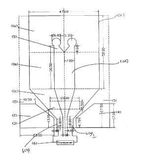
Referring to figure 1, a general geometry of an end driven antenna and its
15 matching circuits, according to an embodiment of the present invention, is
indicated
generally by numeral 1. In this diagram all dimensions are indicated in
millimeters. The
antenna comprises a planar loop element having a generally rectangular outer
perimeter
1 (e) and a slot 1 (d) defining an inner perimeter, the mid portion 1 (b) of
the slot-loop
structure providing a major radiation portion of the antenna; a loading
structure 1(a)
2o having a double ring configuration extending from one end of the slot 1
(d), the loading
structure for top loading the radiation portion; and an impedance matching
portion 1 (c)
for coupling a feed 6 to the major radiation portion 1(b). The antenna is
preferably
etched on a copper clad planar dielectric member, such as an FR4 printed
circuit board
4
CA 02263055 1999-02-26
(5). The FR4 material is only for supporting the antenna. The antenna may be
coupled to
a coaxial connector at the feed end of the antenna.
The double ring top loaded configuration ( 1 a), provides an inductive top
load that
shrinks the overall antenna size, provides wideband potential, and improves
radiation
efficiency. The double rings have a diameter of approximately 3mm to 15 mm,
but are
not limited to this size as shown in Fig.l. The middle part (lb), which is the
major
radiation portion, comprises a central slot structure with its longitudinal
axis aligned
along the longitudinal axis of the antenna such that an electromagnetic field
is developed
between the slot and the E-field normal to the metal edge and separates the
radiation
1o portion into the arms of the loop. The impedance transformation section
1(c) is
comprised of a pair of tapered elements each coupling a feed 6(a) and 6(b) to
a respective
arm of the loop element. The impedance transformation section also behaves
like a
radiation portion. Note that sections ( 1 a), ( 1 b), and ( 1 c) are
distinguished from each other
by dashed lines as shown in Fig.l .
First and second patch elements (2) and (4) are formed proximate the
respective
outer edges of the impedance transformation element. The patch elements (2)
and (4) are
closely coupled to the impedance transformation portion (lc) and are employed
as
distributed matching components. They provide wide bandwidth performance in
conjunction with the top-loaded structure. The patches (2) and (4) are formed
on the same
2o side of the printed board as the matching components. Either patch (2) or
(4) can be, but
are not limited to the shape and size as shown in Fig.l, as long as a proper
matching is
achieved through the coupling effect.
5
CA 02263055 1999-02-26
A third patch element (3) is used to provide a capacitive coupling between
both
portions of the part (lc), which cancels the inductive part of the impedance
looking into
the part ( 1 c) towards the radiation portion over a wide frequency range.
Therefore, even
wider bandwidth is achieved. This patch, being considered as a distributed
matching
component as well, it can be, but is not limited to the other side of the
printed circuit
board. Also, it can be, but not limited to the shape, size, and position as
shown in Fig.l.
In use an RF signal from a transceiver or the like is coupled to the
respective feed points
thereby inducing a current in the antenna, alternatively a current induced in
the antenna
from a received signal is supplied to the transceiver (6).
1 o Referring to Fig. 2 a filrther embodiment of a top loaded structure is
shown. The
top loading structure in this embodiment comprises a U-shaped narrow slot, the
arms of
the U extending into the respective dipoles sections 7(b) and the base of the
U extending
across the end of the slot in the section 7(a). The narrow slot has a length
of
approximately half a wavelength at the center frequency of antenna. The U-
shaped
narrow slot provides an inductive top loading for the antenna. Thus, the
antenna size is
reduced but its radiation efficiency is increased. In addition, the antenna
with such top
loaded configuration has a wide bandwidth potential. 'The other parts are the
same as
those in Fig. 1. The top loading structure may be a single ring as indicated
by numeral
(25) in figure 2 or a double ring configuration as indicated in figure 1.
2o Figure 3 shows the frequency response of the antenna configuration
described
with respect to Figurel, with approximately 85% of the bandwidth covering
1.7GHz to
4.3 GHz.
6
CA 02263055 1999-02-26
Figure 4(a) shows the radiation pattern of the bi-directional antenna as
described
in Figure 1 with a 70° beam width in both a forward and rear direction.
Figure 4(b) shows
the corresponding H-plane radiation pattern. These patterns are very suitable
for PCS
systems, on street scenarios or corndor applications.
As shown in Figure 5, an end driven antenna according to a further embodiment
of the invention includes a ground plane (20) spaced from the radiation
portion of the
antenna described in figure 1. The ground plane causes the antenna to have a
unidirectional radiation pattern as shown in Figures 6(a) and 6(b). It may be
noted that
the rigid dielectric shown in figure 1 may be replaced by for example air if
the copper
1o sections are sufficiently rigid.
Figure 7 shows a balanced 2-element antenna array structure which is comprised
of two end driven antennas connected at their driving points to form a center
fed antenna.
The driving point of the array is fed by coplanar transmission lines
comprising a pair of
outer transmission lines 9(b) and an inner transmission line 9(a), both
extending from an
edge of the substrate to the driving point. The inner conductor 9(a) is
connected to a
common feed point (A) of the radiation elements ( 10) and ( 11 ) which are
electrically
connected in parallel to form a balanced array. The outer conductors 9(b) are
connected to
respective center feed points (B) and (C) o f the radiation elements ( 10) and
( 11 ). In this
configuration, a ground plane is also used to direct the radiation. The
radiation portion
2o can be any configuration but is not limited to the ones described in Figure
1 or Figure 2.
Figure 8 shows a 4-element antenna array having a balanced structure according
to an embodiment of the invention. In this configuration, the antenna is also
end-fed,
however the RF signal is applied along a coplanar transmission line (12) to
the radiators.
7
CA 02263055 1999-02-26
Radiators ( 13) and ( 14) are electrically connected in parallel to form a
balanced sub-array.
Then, this sub-array is cascaded with about 0.65 wavelength coplanar
transmission line
(15). The other sub-array consisting of radiators (16) and (17) is terminated
at the other
end of the coplanar line (15). The radiation elements (13), (14), (16), and
(17) can be any
configuration, but are not limited to the ones described in Figure 1 or Figure
2.
Figure 9 shows a 2-element antenna array with a side feed configuration
according to another embodiment of the invention. The RF signal is fed along a
microstrip transmission line (18), with the ground of the microstrip line
(18b) connected
to the center of the top load edge (D). The microstrip line is formed by the
conductor part
to (18a) and part of the radiation element (19). The transmission line is
terminated at the
point (E) through a via. The radiation element (19) can be any slot-loop
configuration, but
is not limited to the ones described in Fig.l and Fig.2.
Figure 10 shows a single element antenna with a bottom side-feed configuration
according to a further embodiment of the invention. The feed structure (21 a)
and (21b)
15 act as a low loss-matching network to provide wide bandwidth performance. A
patch (22)
distinguished from (21b) by a dashed line is used as a distributed matching
component. It
provides a capacitive coupling and cancels the inductive part of the impedance
looking
into the radiation portion. Note that this patch is different firm the patch
(3) as shown in
Fig.l, since it is not an isolated patch. The RF signal is fed through the
matching network
20 (21) and through a via (23) to a radiation element (24), which can be any
configuration,
but is not limited to the ones described in Fig.l and Fig.2.
Figure 11 shows an 8-element antenna array with back-feed configuration,
according to a still fiu-ther embodiment of the invention. In this, embodiment
two 4-
CA 02263055 1999-02-26
elemet arrays as described in figure 8 are combined. For convenience, the
arrays shall be
referred to as top and bottom arrays, with both arrays formed on one of the
surfaces of a
dielectric member, referred to as the top layer. The arrays are connected by a
micro-strip
line extending between the feed points of the two arrays. The top and bottom
copper
~ layer of the dielectric member constitute the microstrip line. To properly
feed the top 4-
element antenna array and the bottom 4-element antenna array, transitions from
coplanar
transmission lines to microstrip lines are made by vias (27) and (32). The
microstrip
lines are constituted by a narrow copper strip (33) connecting the two arrays
on the top
layer and a wide copper strip (26) on the bottom layer (indicated by dashed
lines) of the
l0 60 mils FR-4 dielectric material. The narrow copper strip on the upper
surface is
comprised of three parts indicated by numerals 28, 29 and 31. Each of these
part has a
different width, thus each constituting a different microstrip line impedance.
A small
patch 30 is arranged at approximately a little more than a half a wavelength
from the top
array, to which a feed is applied.
The first microstrip (28)/(26) is a 70.7-Ohm quarter wavelength line that
transforms the 50-Ohm impedance looking into the top 4-element antenna array
to 100
Ohm. This 100 Ohm impedance is transformed fiuther to the same impedance
(i.e., 100
Ohm) by the middle microstrip (29)/(26), which is half wavelength long and
provides 180
degrees phase shift. This 100 Ohm is then shunted with another 100 Ohm
impedance
2o transformed by the bottom microstrip (31 )/(26) from the 50 Ohm impedance
looking into
the bottom 4-element antenna array to provide a 50 Ohm at the center of the
small patch
(30).
CA 02263055 1999-02-26
The patch (30) is also used to provide slight impedance tuning. A short cable
is
used to feed and/or pick-up an RF signal to and/or from the 8-element antenna
array,
respectively by connecting its center conductor to the top copper patch (30)
via a hole and
its outer shielding conductor to the bottom copper strip (26).
Thus, it may be seen that this invention provides a significant improvement of
the
prior art for the following reasons.
The double ring top loaded structure (la), as shown in Fig. 1, provides wide
bandwidth potential, smaller size, and highly efficient radiation capability.
The half wavelength U-shaped top-loaded structure, as shown in Fig.2, provides
1o wide bandwidth potential, smaller size, and highly efficient radiation
capability.
Matching patches (2), (3), and (4) as shown in Fig. l and Fig.2 are employed
to
provide extra wideband performance.
The simple and novel feed structure (9), by making use of a coplanar
transmission
line and electrically parallel connected radiation components as shown in Fig.
7, is used
15 to minimize the insertion loss of the RF signal due to the feed structure,
simplify the
manufacturing, and provide flexibility in various applications.
A series feed structure with coplanar transmission lines (12) and (15) as
shown in
Fig.8 is applied to the antenna array to achieve less insertion loss of the RF
signal,
simplify the manufacturing, and provide flexibility in various applications.
2o A side feed structure (18), by making use of a microstrip line and the
radiation
component as shown in Fig.9, is employed to provide flexibility of feeding the
RF signal
to the radiation elements for the applications of large antenna array.
CA 02263055 1999-02-26
The matching patch (22), as shown in Fig.lO, in conjunction with a feed
structure
(21 ) (being also considered as the matching network) provides wide bandwidth
performance and less insertion loss. The bottom side-feed configuration makes
the
antenna easily manufactured and the RF signal very conveniently fed into the
antenna
from the bottom.
The top and bottom microstrip (28)/(26) and (31)/(26) as shown in Fig.l l,
respectively are quarter wavelength impedance transformers to transform the 50
Ohm
impedances (looking into the top and bottom 4-element antenna arrays) to 100
Ohm. The
middle microstrip (29)/(26) provides 180 degrees phase shift. The patch (30)
is used to
to provide slight impedance tuning. A short cable is used to feed and/or pick-
up an RF
signal to and/or from the 8-element antenna array, respectively by connecting
its center
conductor to the top copper patch (30) via a hole and its outer shielding
conductor to the
bottom copper strip (26).
Although the invention has been described with reference to certain specific
embodiments, various modifications thereof will be apparent to those skilled
in the art
without departing from the spirit and scope of the invention as outlined in
the claims
appended hereto.
11