Note: Descriptions are shown in the official language in which they were submitted.
CA 02263061 1999-02-26
L
243P58CA
FTFT,I~ OF THE INVENTION
This invention relates to the field of delay
locked loops, and in particular to a novel delay
element.
BACKGROUND TO THE INVENTION
Delay locked loops are used to control the
timing of an internal clock signal, to match that of an
input or external clock signal. Typically an external
clock signal is passed through a delay line, where the
external clock signal is delayed for a controllable
time. The output signal of the delay line is applied to
a circuit to be clocked via a clock distribution tree.
One of the clock signals from the distribution tree (the
internal clock signal) is applied with the external
clock to a comparator, which determines any phase
difference. The difference is used to generate delay
line control signals, which are applied to the delay
line so as to cause the delay to vary and thus minimize
any phase difference between the external clock signal
and the internal clock signal.
Typically the delay line is formed of coarse
delay elements and one or more fine delay elements. One
or more coarse delay elements are connected in series
with a fine delay element. The fine delay element can
be adjusted to the maximum time delay of one coarse
delay element. A system which uses this structure is
described in U.S. patent application Serial No.
09/106,755 filed June 30, 1998, and entitled "Process,
Voltage and Temperature Independent Switched Delay
Compensation Scheme", invented by Gurpreet Bhullar et
CA 02263061 1999-02-26
al, which is incorporated herein by reference.
In delay lines of this type, plural inverters
are connected in series between an input for receiving
the input clock and an output. Switches controlled by
the delay line control are switched so as to bypass
various ones of the inverters, and thus control how many
inverters the external clock signal has to pass through.
However, it has been found that since even the
fine delay is controlled in steps, there is some fitter
remaining. This is because in attempting to maintain
the DLL setting about a lock point, the DLL control
circuitry may attempt to add and remove one fine delay
element continuously. If one fine control step does not
set the delay to cause the internal clock signal to be
exactly in phase with the external clock, there will be
fitter about the lock point.
It has also been found that the fine delay line
cannot always compensate for one coarse delay element
since the coarse element delay can have a longer delay
than the maximum that can be provided by the dynamic
range of the fine delay control due to temperature and
voltage conditions.
It has also been found that noise on the power
supply rails can cause fitter in the output signal of
the delay line, especially in the case of RC-based
inverter delay lines.
The digital delay line also takes up significant
integrated circuit area, due to the resistors and
capacitors required to provide the digital delay line.
3o It is also desirable to have as large a dynamic
range as possible. This dynamic range is limited in a
2
CA 02263061 1999-02-26
delay line having fixed coarse and fine delay elements.
Furthermore, each delay element of the delay line will
experience large variation of delay with variations in
temperature and voltage.
SUMMARY OF THE INVENTION
The present invention has several advantages
over the digital delay line described above. In a
comparison between the above described digital delay
line, in a prototype which had five delay elements to
provide a certain delay variation, only two elements
were required using the present invention to achieve
approximately the same dynamic range. Thus there is
substantial improvement in dynamic range of each
element.
The present invention also takes up smaller
integrated circuit chip area than the above-described
digital delay line, for approximately the same delay,
since plural resistors and capacitors are not required.
The dynamic range increases with decreasing
frequency in the present invention, which is the
opposite of that of the digital delay line, for which
more and more elements would be required to make up the
increased delay time that would be required in a low
frequency device and for test purposes.
The control voltages used in the present
invention can be made very accurate and immune to
temperature and voltage variations. The delay is thus
substantially immune to process variations.
The present invention uses analog delay
elements, instead of digital delay elements of the prior
art.
3
CA 02263061 1999-02-26
In accordance with an embodiment of the present
invention, a method of delaying an input clock signal
comprising:
(a) receiving a digital clock signal,
(b) applying the digital clock signal to an
analog delay element having both coarse and fine delay
control inputs,
(c) applying both coarse and fine delay control
signals to the respective coarse and fine delay control
l0 inputs for controlling an amount of fine and coarse
delay through the delay element,
(d) outputting a digital clock signal delayed
from the input clock signal by an amount equal to the
sum of the fine and coarse delays through the delay
element.
In accordance with another embodiment, a delay
element for simultaneous coarse and fine control of
delay of an input clock signal comprising:
(a) a ramp signal generator for generating a
ramp signal having repetitive ramps with slopes which
start substantially coincident with first edges of the
input clock signal,
(b) a circuit for varying the slopes of the
ramps of the ramp signal for controlling coarse delay
within the delay element,
(c) a circuit for receiving a controllable
threshold voltage for controlling fine delay within the
delay element, and
(d) a circuit for providing an output clock
signal having first edges which are substantially
coincident with the ramp signal attaining a value having
a predetermined relationship with the threshold voltage
and second edges which are substantially coincident with
4
CA 02263061 1999-02-26
the second edge of the input clock signal.
In accordance with another embodiment, a delay
line for receiving an input clock signal and internally
delaying the input clock signal to produce an output
clock signal, the delay line comprising:
(a) an analog delay element having an input for
receiving the input clock signal and an output for
providing the output clock signal, and having a first
delay adjustment input and a second delay adjustment
input,
(b) a first bias voltage generator for providing
a first bias voltage to the first delay adjustment input
of the analog delay element,
(c) a second bias voltage generator for
providing a second bias voltage to the second delay
adjustment input of the analog delay element, and
(d) a delay line control circuit for providing
first and second control signals to the first and second
voltage bias generators respectively.
In accordance with another embodiment, a delay
element having an input terminal for receiving an input
clock signal to be delayed and provided as an output
clock signal to an output terminal, the delay element
comprising:
(a) a first input node,
(b) a circuit for generating a ramp voltage on
the first input node,
(c) a second input node for receiving a
reference voltage,
(d) a circuit for comparing a ramp voltage level
at the first input node with the reference voltage at
the second input node, and for providing an output
signal, and
(e) an output stage for coupling the output
signal to the output terminal comprising a circuit for
5
CA 02263061 1999-02-26
receiving the input signal for selectively enabling and
disabling the output stage.
In accordance with another embodiment, a method
for delaying a clock signal through a delay line having
at least one delay element comprising the following
steps:
(a) receiving a digital input clock signal first
edge,
(b) generating a first ramp voltage at a first
node in response to the presence of the clock signal,
the ramp voltage having a slope which is dependent on a
current which is controlled by a bias voltage,
(c) generating an output voltage first edge at a
second node in response to a comparison between the
first ramp voltage and a predetermined threshold voltage
level,
(d) generating a digital output clock signal
first clock edge in response to the output voltage first
edge at the second node,
(e) receiving a second edge of the digital input
clock signal, and
(f) generating a digital output clock signal
second clock edge in response to second edge of the
digital input clock.
BRIEF DESCRIPTION OF THE DRAWINGS
A better understanding of the invention will be
obtained by a consideration of the detailed description
below, in conjunction with the following drawings, in
which:
Figure lA is a block diagram of a delay element
of the present invention in its most basic form,
Figure 1B illustrates waveforms that may be
observed in the circuit of Figure lA,
Figure 2 is a graph used to illustrate how the
circuit of Figure 1 controls delay,
6
CA 02263061 1999-02-26
Figure 3 is a block diagram of a delay line with
two analog delay elements constructed in accordance with
an embodiment of the present invention,
Figure 4 is a schematic diagram of a delay
element constructed in accordance with an embodiment of
the present invention,
Figure 5 is a schematic diagram of a coarse
delay control signal generating circuit in accordance
with an embodiment of the present invention,
Figure 6 is a schematic diagram of a fine delay
control signal generating circuit in accordance with an
embodiment of the present invention,
Figure 7 is a plot illustrating waveforms at
various locations of the circuit of Figure 4 for a
particular coarse and fine setting,
Figure 8 is a plot illustrating waveforms at
various locations of the circuit of Figure 4, showing
two different coarse delay settings, and
Figure 9 is a plot illustrating waveforms at
various locations of the circuit of Figure 4, for
different fine delay settings.
DETAILED DESCRIPTION OF PREFERRED EMBODIMENT
With reference to Figures lA and 1B, a capacitor
101 is connected in series with a constant current
source 103, node N1 forming their junction. Capacitor
101 can be implemented by using the intrinsic
capacitance of node N1 which includes the input
capacitance of a comparator 111 which is also connected
to node Nl. The source-drain circuit of a field effect
transistor (FET) 105 is connected in parallel with the
capacitor. An external clock signal IN is applied to
the gate of the field effect transistor (FET) 105, shown
in Figure 1B as the signal 107.
The capacitor will charge substantially linearly
as long as the FET 105 is nonconductive. For the n-
7
CA 02263061 1999-02-26
channel type FET shown, while the external clock signal
is at low logic level, the source-drain circuit of the
FET will be nonconductive. While the external clock
signal is at high logic level, the source-drain circuit
of FET 105 will be conductive, discharging capacitor
101. The result is that a continuous ramp signal is
generated on every clock cycle, shown in Figure 1B as
signal 109. The signal 109 is applied from node N1 to
one input of a comparator 111, which has a reference
voltage VT applied to its other input. As shown in
Figure 1B, the voltage at node N1 surpasses VT as the
ramp increases at a time td.
The value of the constant current controls
whether the capacitor will charge either faster or
slower thereby controlling the slope of the node N1
voltage vs time delay curve shown in Figure 2. The
current source therefore controls the coarse delay
characteristic of the delay element.
For example, assuming that the constant current
2o source 103 provides a certain value of current, the
capacitor will charge at a particular rate and establish
one of the charge rate (slope) curves shown in Figure 2.
When the capacitor discharges due to the input signal to
the gate of FET 105 going high and causing FET 105 to
conduct, the output to the comparator will go to high
logic level. After the input signal goes to low logic
level (time ta) the FET 105 switches off, and capacitor
101 will begin to charge. The ramp signal 109 is
applied to the noninverting input of the comparator.
The output of the comparator 111 remains at low logic
level until the ramp voltage reaches the voltage value
applied to its other input, VT, at which time its output
signal switches to high logic level. The difference in
time between the trailing edge of the signal at IN and
the time at which the comparator 111 generates a
8
CA 02263061 1999-02-26
trailing edge to its output signal on node N2 represents
the coarse delay time td.
It may be seen that by controlling the capacitor
101 charging current the time delay tdcan be controlled
to a desired coarse delay timing value.
The voltage VT applied to one of the inputs of
comparator 111 controls the operating point on the curve
in Figure 2, and therefore controls the fine delay
characteristic of the delay element.
Thus, for a fine delay increase, the voltage
causes the delay time to increase from tl to t2,
determined by a charge of the operation point on the
slope of the particular coarse delay curve. For a
coarse delay increase, the coarse delay curve slope
changes the time delay thus charging e.g. from t, to t3.
For both a coarse and fine time delay, both the coarse
delay curve slope changes and the operating point on the
curve changes the time delay charging from tl to t4.
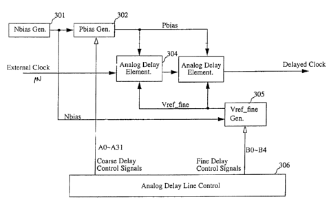
The basic concept of the analog delay element
which was described above can be embodied in a delay
circuit, the block diagram of which is shown in Figure
3. An analog delay element 304 (more than one can be
coupled together as shown in Figure 3) has an external
clock applied to it at IN, as well as a coarse delay
control signal Pbias generated by a Pbias generator 302,
and a fine delay control signal Vref_fine generated by a
Vref_fine generator 305. The Pbias signal is used to
control the constant current value described with
reference to Figures 1A, 1B and 2, and is thus a coarse
delay control signal. The Vref-fine control signal
corresponds to the VT signal applied to the comparator
of Figure lA, and thus is a fine delay control signal.
The delayed external clock signal is shown at the output
of the delay elements as Delayed Clock.
An Nbias signal generator 301 is used to provide
9
CA 02263061 1999-02-26
a bias signal for operation of certain FETs in the Pbias
generator 302 and in the Vref-fine generator 305, and
will be described in more detail later.
An analog delay line control circuit 306 outputs
coarse delay control signals AO - A31 for controlling
the Pbias generator, and also outputs fine delay control
signals BO - B4 for controlling the Vref_fine generator,
as will be described in more detail later.
The analog delay line control responds to
l0 externally supplied signals (not shown) which designate
e.g, a phase mismatch between an external clock and the
delay clock. The internal clock is typically derived
from the external clock. As a result the analog delay
line control outputs coarse delay control signals which
causes the Pbias generator to input a signal to the
coarse delay control input of the analog delay element
(or coarse delay control inputs of a series of analog
delay elements). This causes the delay time of the
delay element or elements to be changed as described
above .
When the time delay is close to the optimum, the
analog delay line control causes the fine delay control
signal to adjust to time delay further until the
external signal to the analog delay line control to
indicate that no further adjustments need be done. In
practice, in the event the coarse delay control controls
the delay too much, this is indicated by the external
signal to the analog delay line control, which backs off
the coarse delay to a point at which the fine delay
3o control is used to adjust the delay of the analog delay
element or series of elements to the optimum delay.
Figure 4 is a schematic diagram of a preferred
embodiment of the delay element 304. Capacitor 101 is
repeated from Figure 1, as is FET 105. The constant
current source 103 is provided by another FET 401. In
CA 02263061 1999-02-26
the preferred embodiment, FET 105 is an n-channel FET,
and FET 401 is a p-channel FET.
Node N1 is applied to the input of comparator
413. The comparator is shown specifically as a current
mirror amplifier of well known construction formed of
FETs 406, 407, 404, 405 and 410. The input to the
comparator is at the gate of an FET 404. The junction
of FETs 405 and 407 form the comparator output, and the
gate of FET 405 forms a second input for the comparator.
l0 A bias voltage Va is applied to the gate of FET 410.
The output signal of the comparator, at node N2,
is applied to the input of an inverter 408, the output
of which is applied to one input of NOR gate 409. The
gate of FET 105 receives the CLK_in signal, which signal
is also applied to the second input of NOR gate 409, as
well as to the gates of pulldown FETs 412 and 414, the
first of which has its source-drain circuit connected in
parallel to the source-drain circuit of FET 410 and the
second of which has its source-drain circuit connected
between node N2 and ground.
In operation, the voltage Pbias is applied to
FET 401, which causes FET 401 to operate in its
saturation region, thus operating effectively as a
constant current source with the value of the current
being controlled by the value of Pbias. Other
controlled current source implementations could be
envisaged by persons skilled in the art.
With reference also to the timing diagram shown
in Figure 7, for the high logic level portion of the
period of the signal CLK-in, the output signal CLK_out
is kept at low logic level due to the action of NOR gate
409. The high logic level of the signal CLK_in also
causes FET 105 to be conductive, thereby discharging
capacitor 101. Node N1 is thus maintained at a low
logic level, as shown in Figure 7. The amount of
CA 02263061 1999-02-26
constant current flowing through FETs 401 and 105 to
ground from the power supply is controlled by the
voltage Pbias. However, with CLK_in being at low logic
level, substantially no current flows through FET 105.
The high logic level voltage applied to FET 414
causes it to conduct, bringing the input of inverter 408
to ground, and the other input to NOR gate 409 to high
logic level. The output of the NOR gate is thus at low
logic level. The high logic level voltage applied to the
gate of FET 412 causes it to conduct, bringing the node
N3 to ground, and thereby disabling the comparator 413.
At the time t0 shown in Figure 7 the falling
edge of CLK_in is applied to the gate of FET 105. As a
result, FET 105 ceases conducting, and capacitor 101
begins charging. A ramp voltage will develop at node N1
as shown in Figure 7, which will surpass the threshold
voltage Vref_fine after a time delay td, where td=tl-to.
The ratio W/L of the gate width W of the FET 105 to the
channel length L of FET 105 should be considerably
larger than W/L of FET 401, so that the voltage between
the gate and the source of FET 105 is larger than that
of FET 401. It should be noted that although the system
is described above with respect to the falling edge of
CLK-in, a dual system could be implemented which
responds to the rising edge of CLK in.
With the CLK-in signal going to low logic level,
FET 412 is disabled, allowing FET 410, having reference
voltage Va applied to its gate, to become operative,
thereby activating the comparator. FET 414 is also
disabled, allowing the output signal on node N2 to
determine the input to inverter 408.
With the fine control voltage Vref-fine applied
to the gate of FET 405, when the voltage at the node N1
reaches and surpasses the Vref fine level, the
comparator 413 conducts more current through the FET
12
CA 02263061 1999-02-26
branch 406, 404, 410, thereby allowing the voltage at
the N2 node to change from low to high logic level, as
shown by curve N2 in Figure 7. This occurs at time tl.
Thus the falling edge of the CLK-in voltage is delayed
from time t0 to the time tl by the time td. This
voltage is inverted in inverter 408, so that the voltage
applied to the NOR gate 409 is the same polarity as that
of the CLK_in signal. Note that the output of inverter
408 does not switch until N2 reaches its switching point
at time tl. Effectively, inverter 408 transforms the
still analog signal at node N2 into a crisp digital
output of CLK out.
When the CLK-in signal again reverts to high
logic level, FETs 105, 412 and 414 are enabled,
IS discharging capacitor 101 (bringing node N1 to ground),
disabling the comparator 413, bringing node N2 to
ground, and causing the output of NOR gate 409 to go to
low logic level. As the CLK-in signal operates at its
particular given frequency, the generation of the ramp
2o voltages at under N1 and N2, resulting in the delayed
output CLK-out are repeated for every cycle. It is
important to note that the delay tdby which the output
signal CLK_out is delayed is determined by the two
control voltages Pbias, determining the coarse delay,
25 and by Vref_fine, determining the fine delay. The use
of the current mirror comparator allows for the accurate
customized control of the delay td based on the control
voltage levels Pbias and Vref fine.
Figure 5 is a schematic diagram of a preferred
3o form of a coarse delay control circuit and Pbias signal
generator. This is comprised of a current mirror
circuit 500, a current control circuit 501 and a
capacitor 510. The current mirror circuit is comprised
of a cascade of three current mirrors connected between
35 a positive power supply rail and ground, formed of PMOS
13
CA 02263061 1999-02-26
FETs 505 and 506, NMOS FETs 507 and 508, and PMOS FET
509. Capacitor 510 is connected between the output of
FET 509 and ground. The control voltage Pbias is
obtained from the output of FET 509.
The current control circuit 501 is comprised of
plural pulldown circuits connected in parallel, each
formed of two NMOS FETs 502A and 503A - 502N and 503N.
The source-drain circuits of each pair of FETs are
connected in series between the node N3 and ground, and
l0 node N3 is connected to the positive power rail through
a PMOS FET 505. Decoded select logic signals AO - AN
are applied to one or more of the gates of FETs 502A -
502N, and a bias voltage nbias is applied to the gates
of FETs 503A - 503N.
The sizes of FETs 503A - 503N are selectively
different from each other so that with a common nbias
voltage applied to their gates, the FETs provide
different resistances. The sizes of FETs 502A - 502N
should be such that they all provide minimal resistance,
and with an enabling voltage applied to their gates,
they act as switches. The overall sizes should be such
that the currents, passing from the positive voltage
rail (VDD) to ground via FET 505, the switches formed by
FETs 502A - 502N through respective FETs 503A - 503N,
should vary (increase) linearly through successive paths
through FETs 503A - 503N. In a preferred embodiment,
there were 32 pairs of FETs 502 and 503. The reference
voltage nbias was received from a conventional DC
reference voltage generator (not shown).
The signals AO - AN can be derived from a
decoder 512 which decodes a signal provided by a counter
(e. g. a 5 bit counter 514 for AN = 32). The counter
receives up and down (UP/DN) control signals from the
delay line control 306 (Figure 3) which compares the
phase of a feedback clock signal with the external
14
CA 02263061 1999-02-26
(clock) signal and generates the UP and DN signals in a
well known manner.
In operation, because the gate bias nbias is a
constant DC voltage, the gate biases of the NMOS FETs
503A - 503N are constant. The currents passing through
these FETs are determined by their sizes. The gates of
FETs 502A - 502N receive the coarse delay control signal
AO - AN referred to with reference to Figure 3. One (or
more, if necessary) of FETs 502A - 502N are switched on,
which causes one (or more) of FETs 503A - 503N to be
connected between the node N3 and ground. As an
example, if only one of the AO - AN control signals is
activated, then a constant current controlled by the
size of a corresponding one of FETs 503A - 503N passes
from the positive voltage rail, through PMOS 505 to node
N3 and through one of FETs 502A - 502N activated by the
AO - An control signal, and a corresponding one of FETs
503A - 503N to ground. Depending on the ratios of FETs
505, 506, 507, 508 and 509 in Figure 5 and FET 401 shown
in Figure 4, a constant current is supplied to the node
N1 of the circuit of Figure 4. As a result, the ramp
slope of the node N1 is determined. In effect, this
ramp slope is determined by the control signals AO -
AN.
The ramp slope at node Nl also affects the ramp
slope at the N2 node, as shown in Figure 8. Figure 8 is
similar to Figure 7 with more detail added, and in
particular illustrates the effect of varying the ramp
slope at node Nl with coarse control. In Figure 8, the
dotted line SL1 shows the steeper slope of the signal at
node N1 when the effective resistance of one of FETs
503A - 503N is smaller (a greater constant current), and
the shallower slope when the effective resistance of
one of FETs 503A - 503N is larger (a smaller constant
current ) .
CA 02263061 1999-02-26
The number of FETs 503A - 503N (and
corresponding FETs 502A - 502N and control signals AO -
AN) to be used in the circuit will be determined by the
required resolution and amount of coarse delay. More
than one FET 503A - 503N can be switched in parallel to
provide different resistances in order to cause a
particular slope which may be intermediate or steeper
than those that may be provided by switching only a
single current path (a single pair of FETs 502 and 503).
The fine delay control voltage Vref fine is
preferably generated in a circuit such as is shown in
Figure 6. A current control circuit 611 is formed
similarly to that of current control circuit 501 in
Figure 5, except as described below. In the present
case, the serially connected FET pairs are 605A and 605N
- 606A and 606N, the drains of FETs 606 being connected
to the sources of FETs 605. The sizes of FETs 606A -
606N are preferably binary weighted; in a preferred
embodiment 5 bits being used so as to provide 32 steps.
Thus the width to length ratio of these FETs (W/L) of
FET 606A was l, the next was 2W/L, the next was 4W/L,
the next was 8W/L and the last of the 5 was 16W/L. The
bias voltage nbias is applied to the gates of FETs 606A
- 606N.
Fine delay control voltages BO - BN are applied
to one or more of the gates of switch FETs 605A - 605N.
Current mirror 613 is comprised of PMOS FETs 601
and 602 and has a pulldown path through resistor 603 and
NMOS FET 604. The output of the current mirror provides
the output signal Vref-fine. The level of Vref_fine is
controlled by the bias current control circuitry 611,
which sets the current flowing from the output of the
current mirror to ground. The bias current control
circuit 611 is formed of a plurality of series connected
to FETs 605A and 606A - 606A and 606N, each series pair
16
CA 02263061 1999-02-26
being connected in parallel between the output carrying
the signal Vref and ground, as shown in Figure 6. A
resistor 612 is also connected in parallel with the
series pairs to provide a load to the output of the
current mirror when none of the FETs in 611 are enabled.
In operation, a constant current passes from the
positive voltage rail, through FET 601, resistor 603 and
FET 604. Due to the current mirror action, a
proportional constant current flows from the positive
voltage rail, through FET 602 and the control circuit
611 according to the size ratio between FETs 601 and
602. The FETs 606A - 606N function as binary-weighted
resistors. Upon enabling of one or more FETs 605A -
605N by the control signals BO - BN, the constant
current flowing through FET 602 is conducted through one
or more corresponding FETs 606A - 606N from the positive
voltage rail. The voltage Vref-fine at the output is
determined by the ratio of the resistances of FET 602
and the single or parallel resistances of FETs 606A -
606N, times the voltage at the positive voltage rail,
e.g. VDD.
Thus in the 5-bit example shown in Figure 6, the
voltage Vref-fine can have 32 different levels by the 5
bit binary combination of the BO - B4 control signals.
The control signals BO - B4 (or BN) can be generated in
a manner similar to control signals AO - AN, using a
counter and decoder in delay line control 306, the
counter being driven by UP/DN signals from a comparison
of the phase of the feedback clock with that of the
external (input) signal.
Figure 9 illustrates the enlarged voltage curves
of Figures 7 and 8, with the effect of variation of the
fine delay control voltage Vref-fine. As previously
noted, at node N1, a particular ramp slope is determined
by a particular coarse control signal AO - AN. To
17
CA 02263061 1999-02-26
illustrate the effects of varying the fine delay,
superimposed on this curve are three values of
Vref_fine, VF1, VF2 and VF3. The intersections of VF3,
VF2 and VF1 with the ramp constitutes delay operating
points t3, t2 and tl of the circuit (shown on the
CLK out curve), which provide delays td3, td2 and tdl
respectively.
The corresponding timing of the signal at node
N2 is also shown, with the rising edges at LEl, LE2 and
l0 LE3 respectively. The respective rising edges of
different time delayed output clock signals are also
shown as LE1, LE2 and LE3 in the curve CLK_out.
Thus the coarse delay signal Pbias applied to
FET 401 of the delay element or series of elements
(Figures 3 and 4), which varies the slope of the ramp at
the node N1 (Figure 4), is controlled by the signals AO
- AN, and the fine delay signal Vref_fine applied to FET
405 in comparator 413 (Figure 4) which varies the
operating point on the slope of the ramp, combine to
vary the time delay in the analog delay element or
elements to a wide degree, avoiding the problems
encountered with the prior art structures described
earlier.
The above has thus described a system which
controls a digital clock signal by means of variable
analog delay elements, to produce a digital output clock
signal with controllable delay.
While the description of the preferred
embodiment described above has indicated the use of
particular conductivity types of FETs for various
purposes and a power supply having the positive polarity
and ground, it will be recognized that opposite
conductivity FETs can be used instead, with a
corresponding change in the polarity of the power
supply, within the scope of the invention.
18
CA 02263061 1999-02-26
A person understanding this invention may now
conceive of alternate embodiments and enhancements using
the principles described herein. All such embodiments
and enhancements are considered to be within the spirit
and scope of this invention as defined in the claims
appended hereto.
19