Note: Descriptions are shown in the official language in which they were submitted.
CA 02263352 1999-02-10
- 1 -
DESCRIPTION
SINGLE CRYSTAL SIC AND A METHOD OF PRODUCING THE SAME
Technical Field
The present invention relates to single crystal SiC and
a method of producing the same, and more particularly to sin-
gle crystal SiC which is used as a substrate wafer for a high
temperature semiconductor electronic element such as a light-
emitting diode, a ULSI (Ultra Large-Scale Integrated circuit,
a rectifying element, a switching element, an amplifying ele-
ment, and an optical sensor, and also to a method of producing
the same.
Background Art
SiC (silicon carbide) is superior in heat resistance and
mechanical strength than existing semiconductor materials such
as Si (silicon) and GaAs (gallium arsenide), and also in high-
temperature property, high-frequency property, dielectric
property, and resistance to environments. In addition, it is
easy to perform the valence control of electrons and holes by
doping an impurity. Moreover, SiC has a wide band gap (for
example, single crystal 6H-SiC has a band gap of about 3.0 eV,
and single crystal 4H-SiC has a band gap of 3.26 eV). For
these reasons, SiC receives attention and is expected as a
CA 02263352 1999-02-10
- 2 -
semiconductor material for a next-generation power device.
As a method of growing (producing) single crystal SiC of
this type, known are a method in which single crystal SiC is
grown by the sublimation and recrystallization method using
a seed crystal, and that in which, in the case of a high tem-
perature, epitaxial growth is conducted on a silicon substrate
by using the chemical vapor deposition method (CVD method),
thereby growing single crystal cubic SiC ((3-SiC).
In the above-described conventional production methods,
however, the crystal growth rate is as low as 1 ~un/hr. Fur-
thermore, the sublimation and recrystallization method has a
problem in that pin holes which have a diameter of several
microns and which pass through the crystal in the growing
direction remain at about 100 to 1,000/csn2 in a growing crys-
tal. Such pin holes are called micropipe defects and cause a
leakage current when a semiconductor device is fabricated.
These problems block a practical use of single crystal SiC
which has superior characteristics as compared with other
existing semiconductor materials such as Si and GaAs as de-
scribed above.
In the case of the high-temperature CVD method, the sub-
strate temperature is as high as 1,700 to 1,900°C, and it is
required to produce a high-purity reducing atmosphere. There-
fore, the method has a problem in that it is difficult to
conduct the method from the view point of installation. Fur-
i
CA 02263352 2002-06-17
-3-
thermore, the method has another problem in that, because
of epitaxial growth, the growth rate is naturally
limited.
Disclosure of Invention
The invention has been conducted in view of the
above-mentioned circumstances of the prior art. Certain
specific embodiments of the invention provide single
crystal SiC of high quality which is little affected by
lattice defects and micropipe defects, and a method of
producing single crystal SiC which can produce such
single crystal SiC easily and efficiently in the view
points of installation and workability, and which can
expedite the practical use of the single crystal as a
semiconductor material.
The single crystal SiC may be characterized in that
a complex in which a polycrystalline plate consisting of
Si and C atoms and having a thickness of 10 um or more is
stacked on the surface of a single crystal SiC base
material is subjected to a heat treatment, whereby
polycrystals of the polycrystalline plate are transformed
into a single crystal.
Polycrystals of the polycrystalline plate may be
phase-transformed by only applying means which thermally
processes a complex consisting of a single crystal SiC
base material and a polycrystalline plate stacked on the
surface of the base material, and which is simple in the
view points of installation and workability, so that a
single crystal which is oriented in the same direction as
the crystal axis of the single crystal SiC base material
is efficiently grown. Furthermore, the thickness of the
i
CA 02263352 2002-06-17
-4-
polycrystalline plate of the complex is set to be 10 um
or more. Even when micropipe defects which impede
transformation of polycrystals of the polycrystalline
plate into a single crystal exist in the vicinity of the
surface of the single crystal SiC base material,
therefore, a single crystal can be grown to a large size
in a range where the single crystal is not affected by
the defects. Consequently, it is possible to obtain
single crystal SiC of high quality which is substantially
free from micropipe defects and defects affected by the
micropipe defects. As a result, it is possible to attain
the effect of expediting the practical use of single
crystal SiC which is superior in high-temperature
property, high-frequency property, dielectric property,
and a high resistance to environments to existing
semiconductor materials such as Si (silicon) and GaAs
(gallium arsenide), and which is expected as a
semiconductor material for a power device.
The method of producing single crystal SiC of the
invention may be characterized in that a polycrystalline
plate consisting of Si and C atoms and having a thickness
of 10 um or more is stacked on the surface of a single
crystal SiC base material, the complex is then subjected
to a heat treatment to transform polycrystals of the
polycrystalline plate into a
CA 02263352 1999-02-10
- 5 -
single crystal and grow the single crystal.
Also the thus configured production method can attain
the effect that single crystal SiC of high quality which is
substantially free from micropipe defects and defects affected
by the micropipe defects is grown easily and efficiently so
that single crystal SiC which is available as a semiconductor
material having a very high performance can be stably produced
and supplied on an industrial scale.
In the single crystal SiC and the method of producing
single crystal SiC of the invention, when the polycrystalline
plate constituting the complex is a polycrystalline (3-SiC
plate grown on the surface of a single crystal SiC base mate-
rial by the physical vapor deposition or the thermochemical
vapor deposition and the thermochemical vapor deposition tem-
perature of the polycrystalline (3-SiC plate is set to be in
the range of 1,300 to 1,600°C, the invention attains an effect
that single crystal SiC of high purity and high quality and
having lattice defects and micropipe defects which are smaller
in number than those of the single crystal SiC base material
can be obtained while entering of impurities between the sin-
gle crystal SiC base material and the polycrystalline plate
on the surface thereof, and diffusion of the impurities are
suppressed.
i I
CA 02263352 2002-06-17
-5A-
In accordance with another aspect of the invention,
there is provided a single crystal SiC including: a
single crystal SiC base material formed into a complex in
which a polycrystalline plate consisting of Si and C
atoms and having a thickness of 10 ~m or more was stacked
on a surface of the single crystal SiC base material, and
the complex was subjected to a heat treatment, whereby
polycrystals of the polycrystalline plate were
transformed into a single crystal.
The single crystal SiC base material constituting
the complex may be single crystal a-SiC.
The polycrystalline plate constituting the complex
may be a polycrystalline a-SiC plate which was grown on
the surface of the single crystal SiC base material by
one of: a physical vapor deposition, and a thermochemical
vapor deposition method. If so, the polycrystalline ~-SiC
plate may be a plate which was grown on the surface of
the single crystal SiC base material by a thermochemical
vapor deposition in a range of 1,300 to 1,600° C.
In accordance with another aspect of the invention,
there is provided a method for producing single crystal
SiC, including the steps of: stacking a polycrystalline
plate consisting of Si and C atoms and having a thickness
of 10 um or more on a surface of a single crystal SiC
base material, forming thereby a complex; and subjecting
the complex to a heat treatment to transform polycrystals
of the polycrystalline plate into a single crystal,
whereby polycrystals of the polycrystalline plate are
transformed and grown into a single crystal.
Single crystal a-SiC may be used as the single
crystal SiC base material constituting the complex.
j
CA 02263352 2002-06-17
-5B-
The polycrystalline plate may include a
polycrystalline ~-SiC plate which is grown on the surface
of the single crystal SiC base material by one of a
physical vapor deposition, and a thermochemical vapor
deposition method. If so, the polycrystalline ~-SiC
plate may be grown on the surface of the single crystal
SiC base material by a thermochemical vapor deposition in
a range of 1,300 to 1,600° C.
A temperature of the heat treatment of the complex
may be conducted at a temperature which is higher than a
thermochemical vapor deposition temperature in a
formation of the polycrystalline ~-SiC plate, and in a
saturated SiC vapor pressure. In this regard, the
temperature of the heat treatment of the complex may be
1,650 to 2,400°C. More particularly, the temperature of
the heat treatment of the complex may be 2,000 to
2,200° C.
Other aspects and features of the present invention
will become apparent to those ordinarily skilled in the
art upon review of the following description of specific
embodiments of the invention in conjunction with the
accompanying figures.
CA 02263352 1999-02-10
- 6 -
Brief Description of Drawings
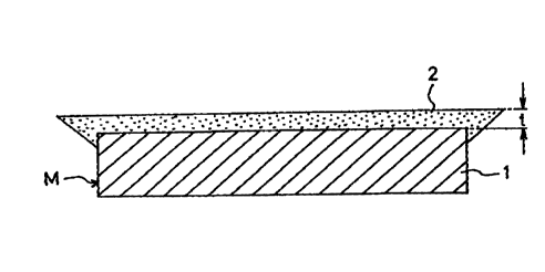
Fig. 1 is a diagram showing a complex before the single
crystal SiC of the invention is heat-treated, Fig. 2 is an
enlarged view of a main portion before the single crystal SiC
of the invention is heat-treated, and Fig. 3 is an enlarged
view of a main portion after the single crystal SiC of the
invention is heat-treated.
Best Mode for Carrying Out the Invention
Hereinafter, an embodiment of the invention will be de-
scribed. Fig. 1 diagrammatically shows a complex M before
single crystal SiC is heat-treated. The complex M is formed
by growing a polycrystalline cubic (3-SiC plate 2 having a
thickness (t) of 10 Eun or more on the surface of a single
crystal hexagonal a-SiC base material 1 (6H type or 4H type)
by the radio frequency magnetron sputtering method (hereinaf-
ter, referred to as the PVD method) or the thermochemical
vapor deposition method (hereinafter, referred to as the ther-
mal CVD method) in the temperature range of 1,300 to 1,600°C.
As clearly shown in a microphotograph of an etched section
of Fig. 2, in the stage of growing the polycrystalline (3-SiC
plate 2, polycrystals 4 of the polycrystalline (3-SiC plate 2
are grown on the surface of the single crystal a-SiC base
material 1 where lattice defects and micropipe defects remain,
and the single crystal a-SiC base material 1 and the poly-
CA 02263352 1999-02-10
crystalline (3-SiC plate 2 are contacted with each other at
crystal faces of different crystal forms so as to show a clear
linear interface 3.
Thereafter, the whole of the complex M is heat-treated
in a saturated SiC vapor pressure and in a temperature range
of 1,600 to 2,400°C, preferably 2,000 to 2,200°C. Therefore,
crystal growth mainly consisting of solid-phase growth, such
as that lattice vibration occurs in the interface 3 to change
the atom arrangement is generated. As a result, as clearly
shown in a microphotograph of an etched section of Fig. 3,
polycrystals 4 of the polycrystalline (3-SiC plate 2 are phase-
converted into a-SiC, and a single crystal 5 which is ori-
ented in the same direction as the crystal axis of the single
crystal a-SiC base material 1 is grown on the polycrystalline
(3-SiC plate 2, with being integrated with the single crystal
of the single crystal a-SiC base material 1.
In the vicinity of the surface of the single crystal a-
SiC base material 1 constituting the interface 3 in the com-
plex M, pin hole-like micropipe defects are scattered. In a
place where such micropipe defects exist, the single crystal
5 which, as a result of the above-mentioned heat process, is
to be grown integrally with the single crystal of the base
material 1 while orienting the polycrystals 4 of the polycrys-
talline (3-SiC plate 2 in the same direction as the crystal
axis of the single crystal a-SiC base material 1 is not suf-
CA 02263352 1999-02-10
ficiently grown, or, even when the single crystal is grown,
micropipe defects and defects affected by the micropipe de-
facts remain in the vicinity of the interface 3, specifically,
in a range L of a thickness of 10 ~.un or less from the inter-
face 3. Single crystal SiC containing such defects has a very
low quality.
In consideration of this point, in the invention, the
polycrystalline ~i-SiC plate 2 is grown in the thickness (t)
of 10 N,m or more on the surface of a single crystal a-SiC
base material 1 of the complex M. According to this configura-
tion, it is possible to grow the single crystal 5 which is
completely free from micropipe defects and defects affected
by the micropipe defects, on the side of the polycrystalline
(3-SiC plate 2 in a range L1 other than the range L where the
above-mentioned defects remain. When the single crystal 5 in
the range L1 used, single crystal SiC of high quality can be
obtained.
The applicant conducted the following experiment on a
sample of single crystal SiC which was produced in the method
described below.
By using a radio frequency magnetron sputtering appara-
tus, a (3-SiC material is placed as a target on the surface of
the single crystal a-SiC base material 1, and a film is grown
for 20 hours in total under the conditions of an Argon (Ar)
atmosphere, 0.1 Torr, and a base material temperature of
CA 02263352 1999-02-10
- 9 -
600°C. Next, the base material is placed in a CVD-SiC lidded
crucible, and a heat treatment is conducted at 2,200°C for 5
hours while maintaining the saturated SiC vapor pressure. The
sputtered surface on the side of the polycrystalline ~i-SiC
plate is slightly polished, and the base material is boiled
in a mixed aqueous solution of calcium hydroxide (KOH) and red
prussiate of potash. Thereafter, the surface is etched. The
surface was observed by a Nomarski interference microscope
with magnifications of 400 times. As a result, no grain bound-
ary was observed.
E~rthermore, X-ray diffraction due to a crystal was con-
ducted on a sample of the single crystal SiC sample produced
as described above, by using an X-ray diffraction apparatus,
and a diffraction pattern in which the abscissa is 28 and the
ordinate is the diffraction strength was measured. As a re-
sult, sharp peaks of the diffraction strength were observed
at regular intervals, at the CuKa, line, and between 40 to 70°
of 28. Therefore, it was confirmed that the sample of the
single crystal SiC sample produced as described above is a
single crystal in which constituting atoms are regularly ar-
ranged.
In the embodiment, the single crystal a-SiC base mate-
rial 1 is used as the single crystal SiC base material. Alter-
natively, for example, an a-SiC sintered member or a single
crystal ~i-SiC member may be used. In the embodiment, the poly-
CA 02263352 1999-02-10
- 10 -
crystalline cubic ~3-SiC plate 2 which is grown on the surface
of the single crystal a-SiC base material 1 by the PVD method
or the thermal CVD is used as the polycrystalline plate. A1-
ternatively, for example, a polycrystalline a-SiC plate, an
SiC sintered member of high purity, or an amorphous plate of
high purity ~1O14atm~~3~ or less may be used, and it is possi-
ble to obtain single crystal SiC of high quality in the same
manner as the embodiment.
As the single crystal a-SiC base material 1 in the em-
bodiment, either of the 6H type or the 4H type may be used.
When the 6H type is used, a single crystal which is converted
from polycrystals of the polycrystalline (3-SiC plate 2 into
a-SiC as the progress of the heat treatment is easily grown
in the same form as that of a single crystal of the 6H type.
When the single crystal base material 1 of the 4H type is
used, a single crystal in the same form as that of a single
crystal of the 4H type is easily converted and grown.
Preferably, the temperature conditions of the heat treat-
ment of the complex M are set to be 1,650 to 2,400°C, and the
process time period is 1 to 3 hours. When the temperature of
the heat treatment is lower than 1,650°C, the kinetic energy
of atoms cannot be given to many SiC constituting the inter-
face. When the temperature is higher than 2,400°C, thermal
energy which is very higher than the decomposition energy of
SiC is supplied and crystals of SiC themselves are decomposed.
CA 02263352 1999-02-10
- 11 -
The entire disclosure of the present application is de-
scribed in the specification, the claims, the drawings, and
the summary of Japanese Patent Application No. 9-207039 filed
on June 25, 1997.
Industrial Applicability
As described above, the invention is a technique that a
complex in which a polycrystalline plate consisting of Si and
C atoms and 10 N.m or more is stacked on the surface of a sin-
gle crystal SiC base material is subjected to a heat treat-
ment, so that polycrystals of the polycrystalline plate are
transformed into a single crystal, and a single crystal ori-
anted in the same direction as the crystal axis of the single
crystal SiC base material is integrally grown to a large size,
whereby a single crystal of high quality which is superior in
heat resistance and mechanical strength and which is substan-
tially free from micropipe defects and defects affected by the
micropipe defects can be produced easily and efficiently.