Note: Descriptions are shown in the official language in which they were submitted.
CA 02263483 1999-02-15
WO 98/10386 PCT/US97/13785
DISC-LIKE DEVICE WITH EAS MATERIAL
Field of the Invention
This invention relates generally to a disc-like
device having electronic article surveillance ("EAS")
material, and pertains more particularly to a disc-like
device having a magnetic material layer detectable by an
EAS detection system.
Background of the Invention
It is well known to provide EAS systems in retail
establishments to prevent or deter theft of goods. In a
typical system, markers, which are secured to goods, are
designed to interact with an electromagnetic or magnetic
field placed at a store exit. If the marker is brought
into the field or "interrogation" zone, the presence of
the marker is detected by the EAS system and an alarm is
activated. Some markers of this type are intended to be
removed at the checkout counter upon payment for the
goods. Other types of markers are deactivated upon
checkout by a deactivation device which changes an
electromagnetic or magnetic characteristic of the marker
so that the marker will no longer be detectable at the
interrogation zone.
One type of magnetic EAS system is referred to as a
harmonic system because it is based on the principle that
a magnetic material passing through an electromagnetic
field having a selected frequency disturbs the field and
produces harmonic perturbations of the selected frequency.
The detection system is tuned to recognize certain
harmonic frequencies, and, if present, causes an alarm.
The harmonic frequencies generated are a function of the
degree of non-linearity of the hysteresis loop of the
magnetic material. Such EAS systems have proven to be
very effective and are in widespread use.
When using this type of system, it has been customary
for employees of a retail establishment to attach the
1
CA 02263483 1999-02-15
WO 98/10386 PCT/US97/13785
markers to the goods at the establishment. Generally,
employees of a store attach markers to goods by means of
a pressure sensitive adhesive layer provided on the
marker, or, when the marker is intended to be removable,
by a mechanical clamping device.
It has been proposed, however, that manufacturers
attach or incorporate the markers in their goods before
shipment to stores. This practice has been referred to as
"source tagging" which means that an EAS marker or "tag"
is applied to goods at the "source" or place of
manufacture of the goods.
This practice has been adopted to help prevent theft
of disc-like devices, such as compact discs ("CDs"). One
example of a surveillance device incorporated in a CD is
disclosed in German Patent No. 42 42 992 A1 ("Cosnard").
The Cosnard patent discloses EAS magnetic strips or
security foil embedded in the plastic portion surrounding
the aperture of the CD. Another example is disclosed in
U.S. Patent No. 5,347,508 ("Montbriand et al.") which
discloses an annular EAS magnetic marker concentrically
oriented and positioned in an annular groove located
around the aperture of the CD.
This placement of EAS strips, foil or markers in a CD
helps to alleviate attaching markers to CDs at the retail
establishment, but may result, however, in hindering the
functioning of the CD, the strip or marker or the CD drive
or player. In addition, if the strip or marker is not
precisely embedded in the CD, a misplacement can cause
interference 'with the functioning of the CD drive or
3 0 player . Further, the aluminum coating of the CD can cause
interference with the output signal level of the EAS strip
or marker thus reducing its signal output which may
prevent detection of the strip or marker by surveillance.
It is, therefore, an object of the present invention
to provide a disc-like device having a magnetic material
layer which provides detection by an EAS detection system.
It is an additional object of the present invention
to provide a disc-like. device having a magnetic material
2
CA 02263483 1999-02-15
WO 98/10386 PCTIUS97/13785
layer which is combineable or integrated with the disc-
like device.
It is a further object of the present invention to
provide a disc-like device having a magnetic material
layer which is not noticeable or removable from the
device.
It is another object of the present invention to
provide a disc-like device having a magnetic material
layer which can be incorporated in the device at the place
of manufacture .
Summary of the Invention
In accordance with the principles of the present
invention, the above and other objectives are realized in
a disc-like device comprising a disc-like substrate of a
light-transmissive material having an information signal
pattern formed on a surface thereof and a magnetic
material layer formed on the information signal pattern of
the substrate.
In a modified form of the device of the invention, a
reflective layer is formed on the information signal
pattern of the disc-like substrate and a magnetic material
layer is formed on the reflective layer.
In a further modification of the device of the
invention, a semi-hard material layer is deposited on the
magnetic material layer which allows for the magnetic
material layer on the device to be deactivatable as well
as reactivatable. This then permits the device to either
be non-detectable or detectable in an EAS detection
system.
In a further modification of the device of the
invention, the disc-like device comprises two disc-like
substrates with a magnetic material layer contained
therebetween.
Brief Description of the Drawings
The above and other features and aspects of the
present invention will become more apparent upon reading
3
CA 02263483 2004-06-23
77496-14
substrates with a magnetic material layer contained
therebetween.
One broad aspect provides a disc device
comprising: a substrate formed of a light transmissive
material and having an information signal pattern formed on
a surface thereof; a reflective magnetic material layer
formed on the information signal pattern on the surface of
said substrate; and a semi-hard material layer comprising a
semi-hard magnetic material formed on said magnetic material
layer, said semi-hard material layer activating and
deactivating the magnetic material layer through the
application of a magnetic field to demagnetize or magnetize
said semi-hard magnetic material to allow for detection and
non-detection, respectively, of the disc device by an
electronic article surveillance detection system.
Brief Description of the Drawings
The above and other features and aspects of the
present invention will become more apparent upon reading
3a
CA 02263483 1999-02-15
WO 98/I0386 PCT/US97/13785
the following detailed description in conjunction with the
accompanying drawings, in which:
FIG. 1 shows a fragmentary cross-sectional view of a
disc-like device in accordance with the principles of the
present invention;
FIG. 2 shows a fragmentary cross-sectional view of a
modified embodiment of the disc-like device of the present
invention;
FIG. 3 shows a fragmentary cross-sectional view of a
further modified embodiment of the disc-like device of the
present invention;
FIG. 4 shows a fragmentary cross-sectional view of
another modified embodiment of the disc-like device of the
present invention; and
FIGS. 5A and 5B show an EAS detection system and
activation/deactivation system for use with the disc-like
device of the present invention.
Detailed Description
FIGS. 1-4 show a disc-like device 10 for use in an
EAS detection system in accordance with the principles of
present invention. In the present illustrative case, it
is assumed that the disc-like device 10 is a compact disc
or "CD", which is a laser-read or optically read data
storing device on which coded information, audio, video or
textual information in digital form can be stored.
As shown in FIG. 1, the disc-like device 10 comprises
a disc-like substrate 12 of a light-transmissive material
or light transmissive synthetic resin such as
polycarbonate (PC), polymethyl methacrylate resin (PMMA),
etc. The substrate 12 is injection molded and has an
information signal pattern which has been formed as a
pattern of pits 18a and lands 18b on a surface thereof.
A magnetic material layer 20 is deposited on the
information signal pattern of the substrate 12, by way of
evaporation, sputtering, etc . The layer 20 is formed over
the surface of the pits 18a and lands 18b so as to cover
the signal pattern on the substrate 12 and has reflective
4
CA 02263483 1999-02-15
WO 98/10386 PCT/US97/13785
properties.
The layer 20, as illustrated in FIG. 1, in general,
is within a range of 1000 A to 5000 ~1 but can also be up
to a thickness of 10, 00.0 A. The thickness of the layer 20
is dependent upon having enough volume of magnetic
material so that a signal therefrom can be provided and
detected by an EAS detection system.
A protective layer 16 may be formed over the magnetic
material layer 20 by a spin coating process to protect the
surface of the disc-like device 10. In general, the
protective layer 16 has a thickness of several microns and
is formed of transparent resin such as ultraviolet ray
curing resin or lacquer.
The magnetic material layer 20 of the disc-like
device 10 of FIG. 1 permits detection of the device 10 in
an EAS detection system in the following manner: The
magnetic layer 20, when subjected to an alternating
magnetic field which exceeds a particular threshold value,
generates a unique harmonic signal. Thus if unauthorized
removal of the device 10 is attempted, the EAS detection
system can detect the unique harmonic signal of the layer
20 and can then generate an alarm.
With the magnetic material layer 20 incorporated in
the device 10 at its place of manufacture, this
incorporation helps to decrease the number of steps
required to provide EAS protection for the device. In
addition, the device 10 can then be immediately displayed
in a retail establishment. Further, with the layer 20
formed on the surface of the device 10, as illustrated in
FIG. 1, EAS surveillance of the device 10 is now possible
without detection of EAS means by a customer, employee,
etc. This prevents both customers and employees from
knowing how the device i0 is protected and further hinders
theft.
In a modified form of the device 10, as best shown in
FIG. 2, a reflective layer 14 is deposited on the
information signal pattern of the substrate 12, by way of
evaporation, sputtering, etc., and is formed over the
5
CA 02263483 1999-02-15
WO 98/10386 PCT/US97/I3785
surface of the pits 18a and lands 18b so as to cover the
signal pattern on the disc-like substrate 12.
The reflective layer 14, for example, can be made of
a metallic material, such as an alloy of aluminum or
silver and can have a thickness in the range of 600 A to
1500 fir.
A magnetic material layer 22 is then deposited on the
reflective layer 14 on the substrate 12. A protective
layer 16 is then formed over the magnetic material layer
22.
FIG. 3 illustrates a further modification of the
device 10 of the invention. In this modification, the
device 10 comprises a disc-like substrate 12, a reflective
layer 14, a magnetic material layer 24, a semi-hard
material layer 26 and a protective layer 16. The magnetic
material layer 24 with the semi-hard material layer 26
deposited thereon allows for the device 10 to be
detectable and non-detectable by an EAS detection system.
In order for the device 10 as shown in FIG. 3 to be
either detectable or non-detectable by an EAS detection
system, the magnetic material layer 24 must be in either
an activated or deactivated state.
To activate the layer 24, an AC degaussing field is
applied to demagnetize the semi-hard material layer 26.
Such demagnetization enables the magnetic layer 24 to
generate a unique harmonic signal. Thus when the layer 24
is subjected to an alternating magnetic field in the EAS
detection area, the EAS detection system will then detect
the presence of the device 10.
For the device 10 to be non-detectable by an EAS
detection system, the magnetic material layer 24 must be
deactivated. To deactivate the layer 24, the semi-hard
material layer 26 is subjected to a pulsed or DC
magnetizing field. Accordingly, if a pulsed or DC field
of an initial level of about 200 Oe or above is applied to
the device 10, the layer 26 is sufficiently magnetized so
that significantly reduced or no harmonic signals from the
layer 24 are detectable. Upon removing the DC field, the
6
CA 02263483 1999-02-15
WO 98/10386 PCT/US97/13785
layer 26 remains magnetized thereby rendering the device
nondetectable.
To reactivate the device 10, the semi-hard material
layer 26 is again demagnetized. This is accomplished by
5 applying an AC degaussing field to the layer 26. Thus,
when an AC degaussing field above about 200 Oe is applied,
the layer 26 becomes sufficiently demagnetized to allow
the magnetic. material layer 24 to generate a harmonic
signal thereby once again rendering the device 10
10 detectable.
Of course, the deactivatable layer 26 could also be
applied to the structure of Fig. 1 where the magnetic
layer 20 serves as both the reflective layer as well as
the EAS magnetic active component.
Where a double sided CD is used, Figures 1 to 3 may
be constructed or laminated back to back to provide the
ability to read both sides of the CD and provide EAS
protection as well as deactivation and reactivation
capability.
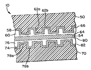
Another modified embodiment of the double sided CD
device 10 is illustrated in FIG. 4, with a first disc-like
substrate 50 and a second disc-like substrate 70 having a
magnetic layer 54 sandwiched between protective layers 60
and 76, respectively, of the two substrates. More
particularly, the protective layer 60, with first top and
bottom surfaces 64 and 66, and the protective layer 76
with second top and bottom surfaces 80 and 82 enclose the
magnetic layer 54 between the first top surface 64 of the
layer 60 and the second top surface 80 of the layer 76.
Similar to the other embodiments, the device 10 has
its first substrate 50 with a first signal pattern of pits
62a and lands 62b and a reflective layer 58 and its second
substrate 70 with a second signal pattern of pits 78a and
lands 78b and a reflective layer 74. Thus the device 10
of FIG. 4 permits information to be stored and read from
two combined substrates while also providing detection of
the device by an EAS detection system. Deactivation and
reactivation of the Figure 4 device may also be provided
7
CA 02263483 1999-02-15
WO 98110386 PCT/US97/13785
by including a semi-hard layer of magnetic material
adjacent the soft magnetic layer 54.
The magnetic layers 20, 22, 24 and 54 of the device
as illustrated in FIGS. 1-4 can comprise an EAS
5 material which can either be a non-magnetostrictive or
magnetostrictive material.
Examples of non-magnetostrictive materials which can
be used for the magnetic material layer are any number of
soft amorphous magnetic materials. For example, amorphous
10 transition metal-metalloid compositions containing Co, Fe,
Si and B with an atomic ratio of Co to Fe of 94:6 can be
used. Examples of such compositions include
CO~4.zsF~'-a.~aSlz.iBie.s arid CO~o.sFea.sSlisBio-
Other materials which may be used include a low
magnetostrictive CoNiFeB based amorphous material
composition such as Cos6Ni16Fe8Bzo and Co44Niz4FelzBzo
Other materials which may be used are amorphous
transition metal-metal compositions selected from the
group comprising Co, Zr and Nb such as Co9oZr5Nb5.
Crystalline material having a NiFe composition such
as Nie1Fe19 may also be used for the magnetic layer.
Magnetostrictive materials which can be used as the
magnetic material layer include amorphous materials
comprising compositions containing Co, Fe, Si and B with
examples including Co39.sFe39.sSi2.lBle.s and Co4.,.4Fe31.6Si2.~B~e.9~
Other examples include compositions containing Co,
Fe, Ni and B such as Co2oFe4oNi2oBzo and ColoFe6oNiloBza
Further magnetic materials can be selected from
compositions including Co, Zr and Nb with an example being
3 0 Co9aZrlo
Magnetostrictive material of a crystalline material
may also be used with compositions selected from the group
comprising Ni~ and Fe . An example includes Ni45Fe5s .
With respect to the magnetostrictive materials,
stress relief annealing may be required to enable the
material to respond to a field. The temperature range and
time for annealing is dependent upon the type of
magnetostrictive material being used, its desired
a
CA 02263483 1999-02-15
WO 98/10386 PCT/US97/13785
thickness and the temperature range of the other materials
comprising the disc-like device (e. g., the type of plastic
substrate, the type of material in the reflective material
layer, etc.).
For the semi-hard material layer 26, semi-hard
material compositions similar to those sold under the
trademarks "Vicalloy" or "Crovac" and available
commercially from Vacuumschmelze GmbH of Hanau, Germany,
may be used. Examples of such compositions include
CoeoNizo and Co48Fe41Vl~ . The layer 26 can have a thickness
in the range of about 0.5 microns to 25 microns and a
coercivity above about 20 Oe and below about 500 Oe.
The device 10 as illustrated in FIGS. 1-4, can be
used in an EAS detection system 100, as illustrated in
FIG. 5A, which detects the presence of the device 10 in a
particular surveillance area 118, e.g., an exit area of a
retail establishment, as indicated by broken lines.
The transmitter portion of the system 100 comprises
a frequency generator 102 with an output being fed to a
power amplifier 104 which in turn feeds a field generating
coil 106. The coil 106 establishes an alternating
magnetic field of a desired frequency in the surveillance
area 118. The amplitude of the field varies depending
upon the system parameters, such as the type of coil, the
size of the surveillance area 118, etc. The amplitude,
however, must exceed a minimum f field so that the device 10
in the surveillance area 118 will detect a field above the
device threshold.
The receiving portion of the system 100 includes a
field receiving coil 112, the output of which is applied
to a receiver 110. When the receiver 110 detects a
particular harmonic content in signals received from the
coil 112 in a prescribed range and resulting from the
device 10, the receiver 110 furnishes a triggering alarm
to an alarm unit 108. The unit 108 activates an alarm to
indicate that unauthorized removal of the device 10 is
being attempted through the surveillance area 118.
In addition, the device 10 as illustrated in FIG. 3
9
CA 02263483 1999-02-15
WO 98/10386 PCT/US97/13785
also has the ability to be detectable and non-detectable
by the EAS detection system 100 by means of an
activating/deactivating system 200. As illustrated in
FIG. 5B, an activating and/or deactivating area 210 is
established by an activating/deactivating unit 208. To
render the device 10 non-detectable, the deactivation
field generator 202 drives a generating coil 206 which
establishes a pulsed or DC magnetizing field through the
area 210. The initial amplitude of the pulsed or DC
magnetizing field must.exceed a minimum level so that the
device 10 in the area will be exposed to a magnetizing
field of a sufficient level to magnetize the semi-hard
material layer 26 of the device 10 to render the device 10
non-detectable. During the deactivation process, the
activation field generator 204 is inactive.
The device l0 as illustrated in FIG. 3 can then also
be rendered detectable by the EAS detection system 100.
An activation field generator 204 drives the generating
coil 206 to establish an AC degaussing field through the
area 210. The initial amplitude of the activation field
must exceed a minimum level so that the device 10 in the
area will be exposed to a decaying AC field of a
sufficient level to demagnetize the semi-hard material
layer 26 to render the device 10 detectable. During the
activation process, the deactivation field generator 202
is inactive.
The device 10 as illustrated in FIG. 3, however, is
not limited to the above deactivation and reactivation
processes but can be activated, deactivated and
reactivated in a variety of ways. For example, a multi-
pole magnet can be used to alter the magnetic state of the
semi-hard material layer 26.
As shown in the illustrated embodiments, the magnetic
material layer as well as the semi-hard material layer
extend over the surface of the disc-like device 10.
However, these layers can extend over only selected areas
of the disc-like substrate and can be formed in a variety
of patterns or designs, such as strips, circles, etc.
CA 02263483 1999-02-15
WO 98/10386 PCT/US97/13785
Further, the device 10 and application of the layers
thereof can also be made by any number of manufacturing
processes. Particularly, a variety of different types of
evaporation and sputtering methods can be used for
applying a magnetic material layer to the disc-like device
10. For example, a planar type sputtering apparatus can
be used. The sputtering method can also include a facing
target cathode type, an ion-beam sputtering type, a laser-
beam sputtering type or a magnetron sputtering apparatus.
The device 10 of the present invention can be any
type and/or size CD, such as CD-ROM, audio CD, mini-CDs,
CD-R, DVD, DVD-ROM, CD-~I, etc. The disc-like device 10 of
the present invention is also not limited to the present
illustrative case, but can also include a phonograph
record or any type of disc-shaped information medium.
In all cases it is understood that the above-
described arrangements are merely illustrative of the many
possible specific embodiments which represent applications
of the present invention. Numerous and varied other
configurations, can be readily devised in accordance with
the principles of the present invention without departing
from the spirit and scope of the invention.
11