Note: Descriptions are shown in the official language in which they were submitted.
i
. CA 02263626 1999-03-12
PIPELINED FAST FOURIER TRANSFORM PROCESSOR
The present invention relates to a pipelined Fast Fourier Transform
processor as is described in the non-characteristic part of claim 1.
Such a pipelined Fast Fourier Transform processor is already known in
the art, e.g. from the published European Patent Application "Pipelined Fast
Fourier Transform processor", publication number 0478128A2 . Therein, a
pipelined Fast Fourier Transform processor is described, including a cascade
of
four Butterfly Arithmetic Units, abbreviated with BAU in the prior art
document.
Each of these units processes data received at its input ports and generates a
pair
of output signals, which are consecutively applied to the input ports of the
next
stage, or in case of the final fourth stage, to memory locations via a
multiplexer.
Within each unit, the output signals , before being delivered to the next
unit, are
temporarily stored in four registers. Two of the cascaded units of the prior
art
document can thus be considered as corresponding to the first and second
arithmetic unit of the present invention, whereas the four registers included
in the
first stage of the prior art, can be considered as corresponding to the
scratch
memory of the pipelined Fast Fourier Transform processor of the invention. The
multiplexer together with the memory locations of the prior art thereby
constitute
the memory arrangement included within the Fast Fourier Transform processor of
the invention.
The units of the prior art processor all include the same building
blocks for performing a radix-two-operation Fast Fourier Transform, hereafter
abbreviated by FFT, operation on their respective input data, as is explained
in
the prior art document.
For some applications, such as for instance in Very High Speed
Digital Subscriber Line transmission and receiving modules, a 512 point real
FFT,
is to be performed in less than 1024 clock cycles, whereby during each cycle
one
data point is read from the memory arrangement into the first arithmetic unit.
As
is well known by a person skilled in the art, performing a 512 point real FFT
in
fact corresponds to performing a 256 point complex FFT, taken into account
some changes such as these explained for instance in the US Patent nr.
CA 02263626 1999-03-12
-2-
5,633,817 "Fast Fourier Transform Dedicated Processor" . However, when
performing a 256 point complex FFT using the architecture of the prior art
processor, too much multipliers are needed for obtaining the target timing
restrictions. Indeed, for performing a 256 point complex FFT, 8 of the prior
art
radix-2 type BAU's have to be passed. Using only two of these BAU's or stages
in cascade, while passing 4 times through the pipeline, already consumes more
than 4X256 clock cycles for reading input data from the memory arrangement to
the first BAU, definitely already exceeding the target timing restrictions.
Therefore,
for complying with the timing restrictions, minimum three of these BAU's are
required to be put in the cascade. Since each prior art BAU includes 4
multipliers,
as is clear from figure 2 of the prior art document, in total thus 12
multipliers
have to be included in the processor. Taken however into account the state of
the
art of the integrated circuit technology at the time of the invention, a total
of 12
multipliers would result in a too large integrated circuit area.
An object of the present invention is to provide a Fast Fourier
Transform processor of the above known type but which succeeds in
compromising both restrictive timing as well as integrated circuit area
requirements.
According to the invention, this object is achieved due to the fact that
said Fast Fourier Processor is further adapted as is described in the
characteristic
part of claim 1.
In this way, two dedicated arithmetic units are provided, a smaller
one, only adapted for performing at least one type of butterfly FFT
calculations,
and a larger one, adapted for performing, besides the aforementioned type, at
least one second type of butterfly FFT arithmetic calculations. In stead of
thus
using three stages in series, now only two of them are needed, a small and a
large one. This solution definitely requires less chip area with respect to
the prior
art solution. With respect to the timing, for performing a 512 point real FFT,
this
solution only requires 3 passes through the cascade or pipeline, as will be
explained more into detail in a further paragraph. The timing is thus within
the
timing specification.
CA 02263626 1999-03-12
-3-
The above mentioned object is also achieved as described in the
characteristic part of claim 2 which is a straightforward alternative of claim
1 and
wherein the first arithmetic unit in which the input data are first treated,
may as
well be the smaller one, whereby the second arithmetic unit which is to be
passed
in the pipelined structure, is the larger one.
Yet a further characteristic feature of the present invention is described
in claims 3 and 4.
For some applications, it may be desirable to first bypass the first
arithmetic unit, after which the second arithmetic unit in the pipeline will
execute
the first FFT related operation. For these applications a simpler control of
the
memory arrangement is obtained, especially when the number of butterfly FFT
operations to be performed by the arithmetic units is non-even, as will be
explained more into detail in the descriptive part of this document.
Still a further characteristic feature of the present invention is described
in claim 5.
If, after the first pass through the pipeline, the final FFT result is not yet
obtained, a second pass will be necessary. This claim indicates that the
pipeline
is always to be followed in the same direction, from the first arithmetic unit
to the
second, after which the memory arrangement is adapted to deliver the
intermediate FFT results back to the first arithmetic unit and so on. This is
the
direction which was also followed in the prior art FFT processor.
Another characteristic feature of the present invention is described in
claims b and 7.
This means that the direction of processing within the pipeline can be
reversed after each pass through the pipeline. The reversal of the direction
after
each pass results in a simpler memory arrangement. Indeed, since the memory
arrangement includes some dedicated locations for storing input data, to be
delivered to the first arithmetic unit, and dedicated locations for storing
intermediate results delivered by the second arithmetic unit, re-use of the
connection between the second arithmetic unit and the memory arrangement
through re-use of these intermediate FFT results by this second arithmetic
unit,
CA 02263626 1999-03-12
-4-
definitely results in a simpler arrangement compared to the case where
additional connections need to be established between the locations for
storing
these intermediate results and the first arithmetic unit.
Further characteristic features of the present invention are mentioned
in the appended claims 8 to 1 1.
The basic computational steps executable by both arithmetic units
thereby consist of a radix-4 type Fast Fourier Transform step, whereas the
extra
alternative steps, executable by the largest of both arithmetic units consist
of a
radix-2 type Fast Fourier Transform step, a radix-2 type Fast Fourier
Transform
step followed by an add/subtract step, and a radix-4 type Fast Fourier
Transform
step preceded by an add/subtract step. All real and complex Fast Fourier
Transform as well as all real and complex inverse Fast Fourier Transforms on
an
amount of points equal to a power of 2, can thereby be realised using a
combinations of these mentioned steps, as is well known from e.g. specialised
literature in the field. From the same literature it is also known that radix-
2 type
as well as radix-4 type arithmetic units both can be realised with merely 4
multipliers. Within the most complex arithmetic unit these four multipliers
may be
shared since only one of the 4 mentioned sets of butterfly Fast Fourier
Transform
arithmetic calculations is to be performed at a time. Therefore the total
amount
of multipliers needed within the subject pipelined Fast Fourier Transform
Processor is 8, being definitely lower than the prior art solution.
The above and other objects and features of the invention will become
more apparent and the invention itself will be best understood by referring to
the
following description of two embodiments taken in conjunction with the
accompanying drawings wherein
Fig. 1 represents a schematic of the pipelined Fast Fourier Transform
Processor FFTP according to the invention, and
Fig. 2 represents a schematic of a straightforward alternative of the
pipelined Fast Fourier Transform Processor FFTP' according to the invention.
CA 02263626 1999-03-12
-5-
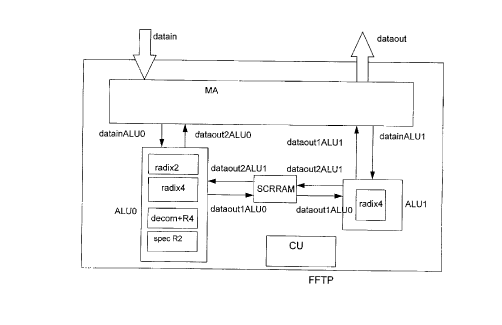
A Fast Fourier Transform Processor FFTP according to the present
invention is schematically depicted in the Fig. 1. This processor includes a
memory arrangement MA, adapted to receive successive samples of input data,
denoted datain, from an input terminal (not shown in Fig. 1 ), to temporarily
store
these successive samples of input data, before delivering them to a first
arithmetic
unit ALUO, to temporarily store intermediate or final Fast Fourier Transform
results, received from either this first arithmetic unit ALUO, or from a
second
arithmetic unit ALU 1, and to deliver the final Fast Fourier Transform results
as
successive output data, denoted dataout, to an output terminal (not shown in
Fig.
1 ).
This memory arrangement MA therefore not only includes the memory
locations as such, but also read/write circuitry and accompanying read/write
addressing encoding/decoding circuitry. Such memory arrangements are
commonly known to persons skilled in the art and will therefore not be
described
into detail in this document.
In the Fast Fourier Transform processor depicted in Fig. l, the first
arithmetic unit ALUO included within FFTP is bidirectionally coupled to the
memory arrangement MA. However other embodiments exist wherein ALUO is
only adapted to unidirectionally receive data from MA. In the embodiment of
Fig.
1, ALUO is adapted to receive from the memory arrangement MA a first set of
first arithmetic unit input data, denoted datainALUO, for performing thereon
one
of the following butterfly FFT arithmetic calculations : either a radix-2 type
calculation, a radix-4 type calculation, a radix-4 type calculation preceded
by an
add/subtract step, or a radix-2 type calculation followed by an add/subtract
step.
The radix-2 type calculation is performed by a block denoted radix2, the radix-
4
type calculation by a block denoted radix4, the radix4 preceded by an
add/subtract step by a block denoted decom+R4, and the radix-2 type followed
by an add/subtract step by a block denoted specR2. It is to be remarked that
all
these functional blocks need 4 multipliers, which may be shared since only one
function is used at a time for treating incoming data. The figure may in this
CA 02263626 1999-03-12
-6-
respect be misleading since some circuitry, for example 4 multipliers together
with some adders/subtracters, are shared by the 4 different blocks.
The result of either one of these 4 arithmetic calculations, performed
on the set of first arithmetic unit input data, datainALUO, is denoted
dataoutlALUO and is delivered by the first arithmetic unit ALUO to a scratch
memory denoted SCRRAM. In some embodiments ALUO is also adapted to
merely bypass its incoming data so that dataoutl ALUO in this case corresponds
to datainALUO.
The scratch memory is adapted to temporarily store these data
dataoutlALUO delivered by ALUO, for delivering them during a following time
step to the second arithmetic unit ALU1 of the Fast Fourier Transform
Processor
FFTP. ALUI is adapted to either bypass these incoming data to the memory
arrangement MA, or to perform a radix-4 type FFT calculation on its incoming
data. The result of either operation is denoted dataoutl ALU 1, and is
delivered by
ALU 1 to the memory arrangement MA.
It is important to mention that the Fast Fourier Transform processor
FFTP of the present invention further includes a control unit, in the figure
denoted
by CU, for controlling the synchronous behaviour of the diverse parts. In
order
not to overload the drawing, the different control signals from the control
unit CU
towards the different parts are however not shown. This control unit CU also
controls the operation of the memory arrangement MA itself, i.e. the timing of
reading data from the input terminal, writing data to the output terminal, the
addresses and locations within the memory where data is to be temporarily
stored, and to be retrieved from , as well as internal reallocation of data
towards
other memory locations within the memory itself. The control signals from the
control unit towards the memory arrangement further enable the memory
arrangement MA to determine whether data received from the arithmetic units
ALUO and ALU 1, consist of a final set of Fast Fourier Transform results, or
whether these are merely intermediate results, which need to pass through the
pipeline formed by the first arithmetic unit ALUO, the scratch memory SCRRAM
and the second arithmetic unit ALU 1, once more. The control signals from the
CA 02263626 1999-03-12
-7-
control unit towards both arithmetic units ALUO and ALU 1 determine which of
the
previously mentioned different operations are to be performed by these
arithmetic units during the consecutive time steps in order to perform a Fast
Fourier Transform on a predetermined number of points, known by the contro
unit.
The control unit CU further controls the operation of the scratch
memory in a similar way as for the memory arrangement. Since the scratch
memory is however much smaller, and only includes a limited number of
memory locations, in one embodiment for instance 32, compared to for instance
512 locations of the memory arrangement MA, the control logic from CU
towards the scratch memory is much less complicated.
For passing through this pipeline a second time, two variants are
possible. In a first variant the pipeline is again followed in the same
direction
from ALUO to ALU1, meaning that data output by ALUI to the memory
arrangement MA, are delivered back by the memory arrangement to ALUO for a
second pass through the pipeline. This may be repeated, until the final FFT
result
is obtained. This is the classical solution, used by most pipelined prior art
processors. Some embodiments of the pipelined processor of the invention such
as the one depicted in Fig. 1 are however adapted to use the pipeline in the
opposite direction after each first pass through it. The second arithmetic
unit
ALU 1 is thereby adapted to receive from the memory arrangement MA, a set of
second arithmetic unit input data, denoted datainALU 1. in case dataoutl ALU 1
is
an intermediate result, datainALUI thus contains the same data as
dataoutl ALU 1. ALU 1 then performs either the same radix-4 type FFT
calculations or a bypass operation on dataoutl ALU 1, thereby generating a
second set of second arithmetic unit output data, denoted dataout2ALU 1, and
delivers this set towards the scratch memory SCRRAM. The latter further
delivers
this data, during a further timestep, towards the first arithmetic unit ALUO,
which,
upon receipt of dataout2ALU 1 starts executing one of the already mentioned
FFT-related calculations, namely a radix-2 type, a radix-4 type, an
add/subtract
followed by a radix-4 type, or an add/subtract followed by a radix-2 type step
or
CA 02263626 1999-03-12
_ $ _
a bypass operation, depending on the control signals from the control unit CU.
The resulting set of data, denoted dataout2ALU0 is delivered again to the
memory arrangement MA. The latter is again adapted to determine, under
control of the control unit CU, whether this received set of data dataout2ALU0
are intermediate or final FFT data. In the former case, this data is again
delivered
either as a new set of datainALUO towards the first arithmetic unit ALUO, or
either
as a new set of datainALU 1 towards the second arithmetic unit ALU 1. In case
dataout2ALU0 are final FFT data, the memory arrangement delivers these data
as the following dataout set towards the output terminal.
Remark that in fact all combinations of passing through the pipeline
are possible, merely depending on the control by the control unit, although
not
all of them are practical. In this respect the "ping-pong" approach, of
continuously alternating directions offers the most advantages concerning
internal memory management of the memory arrangement. If, for instance the
initial data are stored in a first part of the memory arrangement MA, then for
executing a 256 point FFT, 3 passes are needed in order to get the result as
will
be explained in the next paragraph. If the sequence ALUO-ALU 1 /ALU 1-ALUO/
ALUO-ALU1 is chosen, the result is stored in a second part of the memory
arrangement directly coupled to ALU1, while the first part of the memory
arrangement, directly coupled to ALUO is at that moment already free for
receiving new incoming data. The logic for reading and writing data to and
from
the memory arrangement is in this case also less complex.
With this reduced set of FFT calculations, namely radix-4 type, radix-2
type, a radix-4 type preceded by an add/subtract step, and a radix-2 type
followed by an add/subtract step, all real and complex FFT and inverse Fast
Fourier Transform, abbreviated with IFFT, calculations on an amount of real
and
complex data constituting a power of 2 , can be realised. Indeed, for complex
FFT and IFFT operations on a number of N points, for which N constitutes a
power of 4, say4" , n times a radix 4-type step has to be performed for
obtaining
the final FFT or IFFT results on these 4" points. For N = 2.4'T', first a
radix-2 type
operation is to be performed, followed by m times a radix 4 step. The radix-4
CA 02263626 1999-03-12
-9-
and radix-2 types slightly differ between the FFT and the IFFT in this sense
that for
instance for decimation -in -time radix 4 or radix-2 steps, an addition is to
be
performed for the FFT, whereas a subtraction is to be performed for the IFFT
For real FFT's for which N constitutes a power of 4, say N = 4" , n-1
times a radix-4 type is to be calculated, followed by a final "special" radix-
4 type,
consisting of the radix-4 type preceded by the add/subtract step. For N= 2.4m,
first a radix-2 type operation is to be performed, followed by m-1 radix-4
type
operations, followed by the "special radix-4 type" operation.
For real IFFT's for which N constitutes a power of 4 say N = 4" , first
an initial "prescan" consisting of a radix-2 type butterfly followed by an
add/subtract step is to be executed, followed by a radix-2 type butterfly,
followed
by n-1 time a radix-4 type. For N= 2.4m ,first this "prescan" step is to be
performed, followed by n times a radix-4 type calculation. Remark that also
for
this "prescan" the radix-2 to be performed, slightly differs from the "basic"
radix-
2 to be performed, in this sense that again additions may be replaced by
subtractions.
A person skilled in the art is adapted to realise detailed embodiments
of all 4 different radix-2 type and radix-4 type blocks by means of
multipliers,
and adders/subtracters. When sharing different basic circuits for realising
these
four blocks, multiplexers have to be inserted. The control of the multipliers,
adders/subtracters and multiplexers included in these subblocks is again taken
care of by the control unit CU.
In Fig. 2 a straightforward alternative FFTP' of a Fast Fourier
Transform Processor according to the invention is depicted. The same basic
blocks as these that were present in the first embodiment are included, namely
a
memory arrangement MA', a scratch memory SCRRAM', a control unit CU', and
two arithmetic and logic units, ALUO' and ALU 1'. The only difference with
respect
to the first embodiment is that the incoming data, denoted with datain', is
now
first processed in the least powerful arithmetic unit, in Fig. 2 being ALUO'.
This
processing step may consist of the radix 4-type operation, performed by
building
block radix4', but may as well consist of a bypass operation as was also the
case
CA 02263626 1999-03-12
-10-
for the first alternative FFTP. First performing a bypass operation may have
certain advantages, with respect to the control of the memory arrangement, for
instance if a non-even amount of operations is to be performed on the incoming
data. In stead of bypassing the final result through the second arithmetic
unit
ALU 1' or ALU 1, it may be more advantageous to first bypass the first
arithmetic
unit ALUO' or ALUO, and to end at the second arithmetic unit ALU 1' or ALU 1
before delivering the dataout. This is depending on the different steps which
need
to be processed in a certain sequence. Which of both solutions will be
implemented in the controller depends on the amount of basic FFT steps to be
executed. This will become clear from the following example
In an embodiment used for very high speed digital subscriber line
transmission and receiving modules, wherein a 512 point real FFT and IFFT are
to be performed, both first and second alternatives FFTP and FFTP' of the Fast
Fourier Transform Processor are combined. FFTP is used for the Fast Fourier
Transform, whereas FFTP' is used for the inverse Fast Fourier Transform. This
means that, if Fig. 1 is taken as the reference figure for the dataflow, in
the FFT
direction, the incoming data enters ALUO, whereas for performing the IFFT, the
incoming data enters ALU 1. The following butterfly FFT calculations are
executed
as shown by the following tables , whereby DIT is the abbreviation for
decimation-in-time, and DIF stands for Decimation -in-frequency
ALUO ALU1 ALUI ALUO ALUO ALU1
DIT DIT DIT DIT add/subtr+bypass
radix-2 radix-4 radix-4 radix-4 DIT radix4
Table 1 : overview of the sequence of operations to be performed on
the incoming data, for performing a 512 real FFT, whereby the data are
processed from left to right through this table. Reference is to be made to
Fig. 1
for the IFFT following butterfly FFT calculations are executed
CA 02263626 1999-03-12
ALU1 ALUO ALUO ALU1 ALU1 ALUO
bypass DIF radix2DIT DIT DIT DIT
+add/sub radix-4 radix-4 radix4 radix4
Table 2 : overview of the sequence of operations to be performed on
incoming data, for performing a 512 real IFFT, whereby the sequence is from
left
to right through this table and reference is made to Fig. 1.
In the FFT transform direction the data thus enters ALUO, and the final
FFT result is delivered via ALU1, to the memory arrangement, whereas the
opposite direction is used for IFFT. Nevertheless a lot of other combinations
are
possible, whereby the control unit is to be adapted each time for realising
the
particular sequences.
A further remark which needs to be made is that for performing the
radix-2 type and radix-4 type of operations, the decimation-in-time steps may
be
replaced by the decimation-in-frequency steps and vice-versa.
Also for performing complex FFT's and IFFT's both DIT as well as DIF
building blocks may be used in the sequence mentioned in a previous
paragraph, whereby even the DIT and DIF blocks may be mixed. The latter
solution is however not practical and will therefore hardly be used.
As already mentioned, a person skilled in FFT transform algorithms is
further adapted to realise different embodiments for performing these radix-2,
radix-4 and special radix-2 and radix-4 building blocks, both for the DIT as
well
as for the DIF variants. Remark that for the DIT, first a multiplication step
is
executed, followed by add/subtraction steps, whereas this sequence is reversed
for the DIF variant. Since such realisations lie outside the scope of this
document
and can for instance be found in specialised literature, these will not be
further
discussed in this document.
While the principles of the invention have been described above in
connection with specific apparatus, it is to be clearly understood that this
description is made only by way of example and not as a limitation on the
scope
of the invention, as defined in the appended claims.