Note: Descriptions are shown in the official language in which they were submitted.
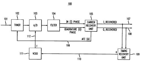
101520CA 02264470 2001-10-051TIMING RECOVERY SYSTEMRelated PatentsU. S. Patent No. 6,192,088, issued February 20, 2001; U. S. Patent No. 5,963,594,issued October 5, 1999; and U. S. Patent No. 5,870,442, issued February 9, 1999.Technical FieldThis invention relates to demodulator arrangements and, more particularly, to timingrecovery in such demodulator arrangements.Backgrognd of the InventionDemodulators are employed in vestigial side band (VSB) receivers to obtain in-phase (I-phase) and quadrature-phase (Q-phase) components of the received VSB signal.Prior known timing recovery systems, however, typically utilized only the I-phasecomponent in attempts at obtaining adequate timing recovery. Additionally prior knownsystems employed an analog synchronous detector in combination with a digital phase-locked loop to recover timing. Such prior systems had relatively limited acquisition rangeand had limited accuracy in determining the location on an incoming synchronization signalin order to recover the timing of the incoming VSB signal.Summary of the InventionThese and other problems of prior known timing recovery systems are overcome byemploying a digital timing recovery system which advantageously employs both thedemodulated I-phase and Q-phase components to more accurately locate thesynchronization signal of the incoming VSB signal. The Q-phase component isadvantageously employed to detect the phase error. The use of the Q-phase componentprovides a more accurate measure of the phase error and results in a larger (wider)acquisition range for timing frequency offset.10152025l i In t ,,,â,,CA 02264470 2001-10-052More speciï¬cally, the timing recovery system of this invention performs symbolclock recovery based on the VSB signal segment synchronization (sync) signal andgenerates a pulse density modulated (PDM) phase difference signal that controls a voltagecontrolled crystal oscillator (VCXO) in the phase-locked loop. This is realized, in oneembodiment of the invention, by correlating received sync segment data with the knownsync signal pattern and searching for "peaks" in the correlation values that are periodic atthe known sync segment data rate. Once the sync pattern is found, the correlation values foradjacent samples are advantageously employed to generate the necessary feedback controlsignal value for the VCXO.Technical advantages of applicantsâ unique invention are that the need for an analogsynchronous detector is eliminated, a more accurate measure than that obtained by priorknown systems is obtained and a wider acquisition range is obtained for timing frequencyoffset.In accordance with one aspect of the present invention there is provided a timingrecovery system for use in a demodulator comprising: correlator means supplied withversions of a recovered in phase component and a quadrature phase component of a receivedsignal for generating a correlation average for each of a plurality of se gments of the receivedsignal; peak detector means for detecting the segment of said plurality having a maximumvalue; means supplied with the quadrature phase component version for generating a phaseerror signal; means responsive to said phase error signal for generating a frequency offsetsignal; ï¬rst enable means being responsive to an output from said peak detector meansindicating that a maximum has been detected for enabling generation of a new value for saidfrequency offset signal; means responsive to said phase error signal and said frequencyoffset signal for generating a timing control -signal representative of phase; and secondenable means being responsive to an output from said peak detector means indicating thata maximum has been detected for enabling supplying as an output a new generated valueof said timing control signal.In accordance with another aspect of the present invention there is providedapparatus for receiving an incoming signal including at least a tuner, an analog to digital10152025CA 02264470 2001-10-053(A/D) converter, a voltage controlled crystal oscillator (VCXO) and a demodulator, thedemodulator including at least a carrier recovery system and a timing recovery system, anoutput from the VCXO being supplied to said A/D, the carrier recovery system generatinga recovered in phase component and a quadrature phase component of the incoming signal,the timing recovery system comprising: correlator means supplied with the recovered inphase component and quadrature phase component of a received signal for generating acorrelation average for each of a plurality of segments of the received signal; peak detectormeans for detecting the segment of said plurality having a maximum value; means suppliedwith the quadrature phase component version for generating a phase error signal; meansresponsive to said phase error signal for generating a frequency offset signal; ï¬rst enablemeans being responsive to an output from said peak detector means indicating that amaximum has been detected for enabling generation of a new value for said frequency offsetsignal; means responsive to said phase error signal and said frequency offset signal forgenerating a timing control signal representative of phase, the timing control signal beingsupplied to adjust the frequency of the VCXO; and second enable means being responsiveto an output from said peak detector means indicating that a maximum has been detectedfor enabling supplying as an output a new generated value of said timing control signal.Brief Description of the DrawingsFIG. 1 illustrates, in simpliï¬ed block diagram form, portions of a demodulatoremploying an embodiment of the invention;FIGS. 2, 3 and 4 illustrate, in simpliï¬ed block diagram form, details of the carrierrecovery unit of FIG. 1;FIG. 5 illustrates, in simpliï¬ed block diagram form, details of the timing recoveryunit of FIG. 1;FIG. 6 illustrates, in simpliï¬ed form, details of the I-Correlator of FIG. 5; andFIG. 7 illustrates, in simpliï¬ed form, details of the Q-Correlator of FIG. 5.1015202530in I amCA 02264470 2001-10-053aDetailed DescriptionFIG. 1 shows, in simpliï¬ed block diagram form details of a portion of ademodulator 100 that employs an embodiment of the invention. Demodulator 100includes, in this example, apparatus 101 for receiving an incoming signal, for example, adigital video signal which, in turn, is supplied to tuner 102 of a type known in the art. Alsosupplied to tuner 102 is an automatic frequency control (AFC) signal, namely, (I), forcontrolling tuner 102 to stay tuned to a desired incoming signal frequency. It should benoted that for completeness of exposition tuner 102 is shown as being adjusted by AFC((1)), however, in many applications adjustment of tuner 102 is not required. An intermediatefrequency signal output from tuner 102 is supplied to analog-to~digital (A/D) converter 103.Also supplied to A/D 103 is a timing signal fat a predetermined frequency. A digital versionof the intermediate frequency signal is supplied to ï¬lter 104. Filter 104 is a matched ï¬lter,of a type well known in the art, which performs matched ï¬ltering, decimation and a Hilberttransform of the digital samples from A/D 103 to yield separate In (I) phase (I-phase) andQuadrature (Q) phase (Q-phase) passband components. The I-phase and Q-phasecomponents are supplied to carrier recovery unit 105. As will be explained in detail below,carrier recovery unit 105 generates an In phase recovered (I-Recovered) component and aQuadrature phase recovered (Q-Recovered) component, as well as, the AFC signal. TheAFC signal is supplied via circuit path 106 to tuner 102, while I-Recovered and Q-Recovered are supplied via circuit paths 107 and 108, respectively, to additional portionsof the demodulator (not shown) and to timing recovery unit 109. In turn, timing recoveryunit 109 generates timing control signal, i.e., phase 3, which is supplied to voltagecontrolled crystal oscillator (VCXO) 1 1 1. VCXO l 1 1 is responsive to timing control signal9 to generate timing signal f, which is supplied via circuit path 112 to A/D 103.FIGS. 2, 3 and 4 show, in simpliï¬ed form, details of an embodiment of carrierrecovery unit 105. Referring to FIG. 2, shown is complex multiplier 201 to which the I-phase and Q-phase signal components are supplied. Complex multiplier 201 inconjunction with SIN/COS look up table 202 demodulates the I-phase and Q-phasesignal components to obtain signals representative of I_demod and Q_demod,respectively. The demodulation is realized by complex multiplication of the I-phase andQ-phase signal components with a complex exponential sequence. The exponentialsequence is supplied by SIN/COS look up table 202 in response to frequency controlsignal Such complex multiplier arrangements used for demodulation are well known1015202530CA 02264470 1999-03-054in the art. The value of I_demod is supplied to one input of combining unit 203 and thevalue of Q_demod is supplied to one input of combining unit 204. An output fromstandard delay (D) unit 205 is supplied to a negative input of combining unit 203 and toan input of combining unit 209. Similarly, an output from standard delay (D) unit 206 issupplied to a negative input of combining unit 208 and to an input of combining unit210. Standard delay units 205 and 206 are, for example, inï¬nite impulse response (IIR)ï¬lters of a type known in the art. Constant a = 2'Wis supplied to multipliers 207 and208 to realize exponential smoothing of outputs from combining units 203 and 204,respectively. It should be noted that W is as large as practical in the tracking mode ofoperation.In this example for carrier recovery, W has a range of 5-14 and for theacquisition mode (a1) W=l2 and for the tracking mode (ao) W=6. Combining unit 209combines the output of multiplier 207 and the output standard delay unit 205 to obtain P.P (ï¬rst average) is an average of I_demod. P is supplied to the 1 input of selector 210,to an input of combining unit 211 and an input of multiplier 212. Similarly, combiningunit 210 combines the output of multiplier 208 and the output standard delay unit 206 toobtain Q. Q (second average) is an average of Q_demod. Q is supplied to the 1 input ofselector 213, to an input of combining unit 214, an input of multiplier 215, to -sgn (sign)(Q) unit 219 and to sgn(Q) unit 218. ,B:2'X is supplied to an input of each ofmultipliers 212 and 215. In this example for carrier recovery, X has a range of 3-12 . Inthe acquisition mode X=4 ( ï¬o ), X=8 ( ,Q) or( I82) X=1O which provide a number of stepchanges in the phase during the acquisition mode of operation, as shown below. In FIG.2, when in the tracking mode [3 is not employed because the values of P and Q are notmodiï¬ed or adjusted. The output from multiplier 212 is an adjusted version of P that issupplied to an input of multiplier 216 and the output from multiplier 215 is an adjustedversion of Q that is supplied to an input of multiplier 217. A signal representative of -sgn (Q) is supplied from -sgn (Q) unit 219 to multiplier 216 and a signal representativeof sgn (Q) is supplied from sgn (Q) unit 218 to an input of multiplier 217. The resultingoutput from multiplier 217 is supplied to combing unit 211, where it is algebraicallyadded to adjust the value of P. The resulting output from combining unit 211 is suppliedto the 0 input of selector 210. The resulting output from multiplier 216 is supplied to2025CA 02264470 2001-11-235combining unit 214 where it is algebraically added to adjust the value of Q. The resultingoutput from combining unit 211 is supplied to the 0 input of selector 213. An output fromselector 210 is supplied to the input of standard delay unit 205 and an output from selector213 is supplied to the input of standard delay 206. The mode of operation, i.e., acquisitionor tracking, is controlled by a "locked" signal supplied to selectors 210 and 213 to select asan output the signal supplied to either the 0 input or the 1 input. Note that in the acquisitionmode (0) the adjusted values of P and Q are selected which enable locking to the carriermore rapidly. In the tracking mode (1) the non-adjusted values of P and Q are used that havebeen obtained by employing the smaller values of on and Again, the use of the non-adjusted values of P and Q provides significantly better tracking of phase in the presenceof phase noise. Generation of the locked signal and the adjustment of parameters cc and [3are described below in relationship to FIG. 3. It is noted that for the acquisition mode ofoperation that on is large in order to obtain the average of P and Q. The use of the largervalue of or is desirable to "lock" onto the carrier phase rapidly. However in the trackingmode on is smaller in value than that used in the acquisition mode. Otherwise, it is difficultto track the phase in the presence of phase noise. Thus it can be shown by employing therelatively large values of on and B relatively fast convergence is obtained initially during theacquisition mode and then relatively quiet operation of the vector tracking ï¬lter of FIG. 2is realized in the tracking mode by employing the smaller values of or and One suchvector tracking ï¬lter is disclosed in above mentioned U. S. Patent No. 5,963,594. Note thaton, [3 and locked are supplied from lock decision unit 303 (FIG. 3).Referring now to FIG. 3, it is shown that P is supplied to an input of combining unit301 while Q is supplied to one input of combining unit 302. Q is also supplied to lockdecision unit 303. An output of standard delay (D) unit 304, namely, Pâ, is supplied to anegative input of combining unit 301, where it is algebraically subtracted from P, toan input of combining unit 308, to an input of combining unit 310 and to lock decisionunit 303. Pâ (third average) is an average of P and is referred to as a second average of10152025CA 02264470 1999-03-056I_demod. An output of standard delay (D) unit 305, namely, Qâ, is supplied to anegative input of combining unit 302, where it is algebraically subtracted from Q, to aninput of combining unit 309 and to lock decision unit 303. Again, in this example,standard delay units 304 and 305 are IIR ï¬lters. Qâ (fourth average) is an average of Qand is referred to as a second average of Q_demod. An output from combining unit 301is supplied to multiplier 306 and an output from combining unit 302 is supplied tomultiplier 307. Also supplied to multipliers 306 and 307 is parameter 5 = 2'2 from lockdecision unit 303. In this example, Z has a range of 12-18 and typically is 16. Theoutputs of multipliers 306 and 307 are adjusted values of the outputs from combing units301 and 302, respectively, and are supplied to combining units 308 and 309,respectively. The adjusted values of P and Q from combining units 308 and 309 aresupplied to standard delay units 304 and 305, respectively, which yield the third andfourth average values Pâ and Qâ, respectively. Lock decision unit 303 is operative togenerate the âlockedâ signal for controlling carrier recovery unit 105 to be in theacquisition mode or the tracking mode and to provide parameters a, ï¬, y and 6.I_demod is supplied to one input of combining unit 310 and Pâ is supplied to anotherinput where it is algebraically subtracted from I_demod. This subtraction of Pâ removesthe direct current (D.C.) pilot signal to yield I_recovered. As indicated Q_demod is alsoQ_recovered. Q_recovered and I_recovered are supplied to other portions of thedemodulator and to timing recovery unit 109.The operational mode, i.e., acquisition or tracking, of carrier recovery system105 and the values of parameters 0t, ,6, 7/ and 5 are determined by lock decision unit303. In the following process y = 2", k = 2'â, S = 2'â and b = To. The lockingdecision is determined by:1r(1Q-l < (IP'| . 2-â )) then/2â= ï¬o, 7 = 70, c=c+1else if ([Q'| < (|P'| . 2"â)) thenCA 02264470 1999-03-057ï¬=ï¬, 7=7,,c=0else/>â=ï¬2, 7=72,c=0end if5 if (c 2 L) thenlocked = 1c=Lxi = Q - 2*âelse10 locked = 0end ifif (locked = 0) thena = a1else15 i a = a0end if6: 50 â aParameters a0,a1, ï¬o, A, /32, yo, 71, yz, éwk, S1, S2, andLare tunableparameters that depend on the particular characteristics of tuner 102 (FIG. 1) that is101520CA 02264470 1999-03-058being employed to receive the incoming signal. Values of these parameters are stored inlock decision unit 303.Note that programmable hysteresis is obtained in the locking decision process bythe selection of the value of L and the use of counter c. Through the selection of thevalue of L the duration of the interval before which a locking decision is made can beadjusted as desired. Additionally, counter c is incremented during a portion of theacquisition decision process and set to zero (0) during other portions of the acquisitionprocess, as indicated above. Once the mode is switched from acquisition to tracking, thevalue of counter c is set to c=L. Thus, the desired hysteresis is realized in switchingfrom the acquisition mode to the tracking mode and also from the tracking mode back tothe acquisition mode. During the acquisition mode the bandwidth is narrower thanduring the tracking mode. This is because a larger value for Ot is employed than in thetracking mode. Further, the phase during the tracking mode is linear because Q is linearand a ï¬xed shiï¬ is realized in the linear phase because k is a ï¬xed value, as shown above.In summary, the parameters in this example for carrier recovery unit 105 are byway of example only, as follows:0:0, (1,: rangeofW:5-14typical values: a0, W=6,a1,W=12;ï¬o, ï¬,,B2: rangeofX: 3 -12typical values: ï¬o, X=4,/1 , X=8,ï¬z , X=10;yo, }/1,}/2, rangeofY: 5- 141020A-ââ.â__........ ._._. . â>â\>CA 02264470 1999-03-059typical values: 70 , Y=6,71, Y=8,}/2 , Y=10;50 range ofZ: 12- 18typical Value: 50, Z=16;k range ofM: 2 - 8typical Value: k, M=4;S1, S3 range ofN: 2 -4typical values: S], N=4,S2, N=2;L range: 16384 - 65536typical value: L=3 2768;b range 0: 10 â 16typical value: O=14.Fig. 4 shows, in simpliï¬ed form, further details of carrier recovery unit 105.Shown is Q being supplied to -sgn (Q) unit 401. The obtained -sign value of Q issupplied to an input of multiplier 402. Parameter [3 is supplied from lock decision unit303 (FIG. 3) to an input of look table 403 and to a one (1) input of selector 404. Anoutput from look up table 403 is supplied to the zero (0) input of selector 404. Look uptable 403 in response to a supplied value of B, outputs a corresponding phase_errorvalue. To this end,101520CA 02264470 1999-03-05102âphase_error =32nwhere B is the bitwidth of frequency control signal (1) and, in this example, has a typicalvalue of B = 16. Typical values of the phase_error, for this example, are from an104302/, andapproximation of the above phase_error equation, namely, phase_error zare13 phase error0 104301 52152 26083 13044 652* ** ** *10 10.The state of the locked signal that is supplied to selector 404 depends on themode of operation of carrier recovery unit 105. As indicated above, locked is 0 for theacquisition mode and l for the tracking mode. The phase_error is multiplied by the -sgn(Q) via multiplier 402 and the result is supplied to multiplier 405 and an input ofcombining unit 406. Also supplied to multiplier 405 is the result of the division of b andy by divider 407. The parameter b = 2'0 and the parameter 7 = 2" . Typical values forb and 7 are shown above. An output from multiplier 405 in supplied to one input of10152025CA 02264470 1999-03-0511combing unit 409 and an output from standard delay (D) unit 410, which is a delayedversion of the output from combining unit 409, is supplied to another input of combiningunit 409, where it is algebraically added to the output from multiplier 405. An outputfrom combining unit 409 is representative of the accumulation of the carrier frequencyoffset and is supplied to an input of standard delay unit 410 and to an input of multiplier411. Standard delay unit 410 is also an IIR ï¬lter, in this example. Parameter b issupplied to another input of multiplier 411 to be multiplied with the output fromcombining unit 409. A resulting output from multiplier 411 is supplied to another inputof combining unit 406 where it is algebraically added to the output from multiplier 402.An output from combining unit 406 is supplied to an input of combining unit 412. Amodulation frequency value (fc) is supplied to a subtracting input of combining unit 412,while a delayed version of an output from combining unit 412 is supplied via standarddelay (D) unit 413 to another input of combining unit 412. Standard delay units 410 and412 are, in this example, also IIR filters. The supplied inputs are algebraically combinedvia combing unit 412 to yield frequency control signal :1). Frequency control signal (1) issupplied to other portions of the demodulator (not shown) and as automatic frequencycontrol signal 4) (AFC) to tuner 102 (FIG. 1). Note that the bitwidth of frequencycontrol signal 4) is typically B = 16.The bitwidth F employed in delay unit 410 (FIG. 4) is determined by:F = O + w,wheremax.carrier. freqoï¬set-23) +1 andsymbolfreq.w = log2(typical values for the max. carrier freq. oï¬set are: i 150 kHz, a typical symbol freq.value is 10.76 MHz and, as indicated above, a typical value for B is 16.FIG. 5 shows, in simpliï¬ed form, details of timing recovery unit 109 of FIG. 1.I_recovered from FIG. 3 is supplied to I-correlator 501, while Q_recovered is supplied10152025CA 02264470 2001-10-0512to Q-correlator 502 and delay unit 503. I-correlator 501 and Q-correlator 502 obtaincorrelated values of I and Q by searching for predetermined patterns in I_recovered andQ_recovered, respectively. Thus, I-correlator 501 yields I_correlated and Q-correlator 502yields Q_correlated. Details of I-correlator 501 and Q-correlator 502 are described belowin relationship to FIG. 6 and FIG. 7, respectively. I_correlated is supplied to multiplier 504where it is squared. Similarly, Q_correlated is supplied to multiplier 505 where it is squared.The squared values of I_corre1ated and Q_correlated are supplied to combining unit 506where they are summed. In turn, the summed values of I_correlated and Q_correlated aresupplied to an input of combining unit 507. An output from multiplier 511 is supplied toanother input of combining unit 507, where it is algebraically subtracted from the input fromcombining unit 506. An output from combining unit 507 is supplied to an input ofcombining unit 508 where it is algebraically summed with an output from registers unit 5 10.The output from registers unit 510 is also supplied to multiplier 511 where it is multipliedby out. In this example, at = 2_W' , where W, has a range of 2-10 and typically is 6. Anoutput from combining unit 508 is supplied to an input of registers unit 510 and to multiplier509. Registers unit 510 includes a plurality of registers in a sequence, in this example, 832registers. It is noted that combining units 507 and 508, registers unit 510 and multiplier 51 1form essentially an IIR ï¬lter. Then, starting with register zero (0) of registers unit 510 andclocking through register 831, the value in each of the 832 registers is IIR filtered insequence and supplied to multiplier 509, where the supplied value is multiplied by ac. Theresulting output from multiplier 509 is a correlation average, which is supplied to peakdetector 512. While cycling through the registers of registers unit 510, peak detector 512selects the maximum value and generates an enable signal only during the duration that thecorresponding register having the maximum value of all the registers during a currentcycle is being clocked. The enable signal is supplied to enable unit 513 and enable unit514. Enable unit 513 is operative to enable standard delay unit 515 to pass the currentvalue at its input to an input of combining unit 516 during the current clock interval,otherwise the last previous value is supplied as an output from delay unit 515. Similarly,10152025CA 02264470 1999-03-0513enable unit 514 is enabled to pass a current value supplied to its input when enabled andto pass the last previous value supplied to its input otherwise.An output from delay unit 503 is supplied to an input of combining unit 517 andto an input of delay unit 518. An output from delay unit 518 is supplied to another inputof combining unit 517, where it is algebraically summed with the output of delay unit503. Combining unit 517 yields at its output the sum two consecutive values ofQ_recovered, which is supplied to multiplier 519. Multiplier 519 multiplies the outputfrom combining unit 517 by ,6â, = 2âX' , where X , has a range of 2-10 and a typical valueof 3. The output from multiplier 519 is a smoothed, i.e., average, value S_in of thesummed values of Q_recovered, which is supplied to an input of limiter 520. The outputS_out of limiter 520 is determined as follows:S_out = S_in, if |s_ml s A, andS_out = sign (S_in) *. 4, if |S_m1 > A,,where A, has a range of 25 -28 and, in this example, is typically 27 and where 6, hasrange of 25 - 28 and, in this example, is typically 27.S_out from limiter 520 is supplied to an input of combining unit 516, where it isalgebraically subtracted from the output from delay unit 515, and to an input ofcombining unit 522. An output from combining unit 516 is supplied to an input of delayunit 515 and to multiplier 521, where it is multiplied by y,. y, = 21â where K has arange of 8-16 and, in this example, a typical value of 10. An output from multiplier 521is a frequency offset value and is also supplied to an input of combining unit 522.Combining unit 522 algebraically subtracts the S_out output from limiter 520 from theoutput from multiplier 521 to yield timing control signal 6. Again, enable unit 514 isenabled by the output from peak detector 512 to supply as an output the current value of6, otherwise the last previous value of timing control signal 9 is supplied as an output.Timing control signal 9 is supplied to VCXO 111 (FIG. 1) and to PDM (not shown).10152025CA 02264470 2001-10-0514Details of Iâcorre1ator 501 are shown, in simpliï¬ed form in FIG. 6. I-correlator 501 isemployed to correlate I_recovered by a predetermined pattern, in this example, 1, -1, 1, -1.When this pattern is found the output from Iâcorrelator 501 is a maximum. To this end,I_recovered is supplied to an input of delay unit 601 and to multiplier 602, where it ismultiplied by 1. An output from multiplier 602 is supplied to an input of combining unit608. An output from delay unit 601 is supplied to an input of delay unit 603 and tomultiplier 604, where it is multiplied by -1. An output from multiplier 604 is supplied to aninput of combining unit 608. An output from delay unit 603 is supplied to an input of delayunit 605 and to multiplier 606, where it is multiplied by -1. An output from multiplier 606is supplied to an input of combining unit 608. An output from delay unit 605 is supplied tomultiplier 607, where it is multiplied by 1. An output from multiplier 607 is supplied to aninput of combining unit 608. Combining unit 608 algebraically sums the outputs frommultipliers 602, 604, 606 and 607 to yield I_correlated.Details of Q-correlator 502 are shown, in simpliï¬ed form, in FIG. 7. Q-correlator502 is employed to correlate Q_ recovered by a predetermined pattern in this example, |J.,-V, pl, -V. When this pattern is found the output from Q-correlator 502 is a maximum. Tothis end, Q_recovered is supplied to an input of delay unit 701 and to multiplier 702, whereit is multiplied by p.. An output from multiplier 702 is supplied to an input of combiningunit 708. An output from delay unit 701 is supplied to an input of delay unit 703 and tomultiplier 704, where it is multiplied by -V. An output from multiplier 704 is supplied to aninput of combining unit 708. An output from delay unit 703 is supplied to an input of delayunit 705 and to multiplier 706, where it is multiplied by V. An output from multiplier 706is supplied to an input of combining unit 708. An output from delay unit 705 is supplied tomultiplier 707, where it is multiplied by ~p.. An output from multiplier 707 is supplied to aninput of combining unit 708. Combining unit 708 algebraically sums the outputs frommultipliers 702, 704, 706 and 707 to yield Q_correlated. In this example, typical values forp. and V are: p.=0.3-0.5 and vz 1.0-1.5.CA 02264470 1999-03-0515All the parameters that are supplied to multipliers in this embodiment are powersof two (2) so that all multiplies can be implemented by utilizing shiï¬s, thereby making iteasier to implement an embodiment of the invention on VLSI, an ASIC or a DSP, as willbe apparent to those skilled in the art.