Note: Descriptions are shown in the official language in which they were submitted.
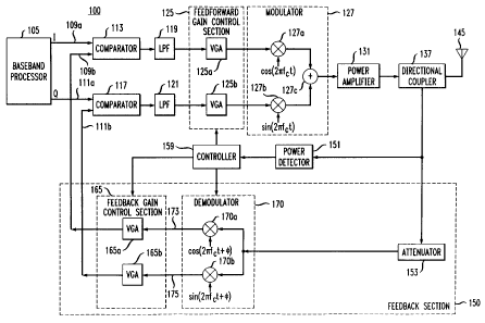
1015202530CA 02265143 1999-03-101TECHNIQUE FOR EFFECTIVELY RENDERING POWER AMPLIFICATION ANDCONTROL IN WIRELESS COMMUNICATIONSField of the InventionThe invention relates to communications systems andmethods, and more particularly to a system and method forrealizing high power efficiency in wireless transmissionand effective control of transmission power.Background of the InventionIt is well known that with no excitation applied to anamplifier, an operating point, known as a "quiescent point"or "DC operating point," is defined in an active region ofthe output characteristics of the amplifier. To providelinear amplification for a radioâfrequency (RF) inputsignal for example, a class A amplifier is normally used,which is typically biased to place the DC operating pointfar enough from both cutoff and saturation regions in itsoutput characteristics. As a result, the input signalexcursions to either side of the operating point do notcause the signal to be cut off or the amplifier to besaturated, thus avoiding introducing distortion into thesignal. However, a major drawback of the class A amplifieris its low power efficiency due to a relatively high DCinput power required by the amplifier, with respect to itsoutput signal power.A class B amplifier is typically biased to cut off ahalfâcycle of an input signal, with an output current flowonly during the positive halfâcycle of the signal. As aresult, the amplifier output is significantly distorted,with respect to the input signal. Thus, a class Bamplifier is unsuitable for a typical linear operation.However, with respect to a class A amplifier, a class Bamplifier affords higher power efficiency as the DC inputpower to the amplifier is relatively low.101520253035CA 02265143 1999-03-10A class AB amplifier, on2the other hand, is typicallybiased in such a way that the output current flows for morethan half of the cycle of the input signal. As a result, aclass AB amplifier behaves like a hybrid between the classA and class B amplifiers. Thus, a class AB amplifiercauses a lower distortion than a class B amplifier (but ahigher distortion than a class A amplifier) to an inputsignal at a high power level. At the same time, the classAB amplifier realizes higher power efficiency than a classA amplifier.A class C amplifier is typically biased in such a waythat the output current flows less than half of the cycleof the input signal. As a result, the class C amplifieraffords the highest power efficiency and, unfortunately,also distortion to an input signal of all of theaforementioned amplifiers.A power amplifier is typically used in a transmitterof a digital wireless communications system, e.g., personalcommunications service (PCS) system, to boost the powerlevel of a digitally modulated signal for transmissionthereof. In wireless communications, the power amplifieris required to afford linear amplification to the signal,without introducing significant distortion thereinto. Assuch, in the prior art, the power amplifier used in awireless transmitter typically operates in a class A and/orclass AB mode to satisfy the linear amplificationrequirement.However, for example, a transmitter in a wirelesstelephone handset is normally powered by a rechargeablebattery having a limited capacity. The usable transmissiontime allowed by the battery before recharging thereofincreases with the power efficiency afforded by the poweramplifier in the transmitter. Since a long allowabletransmission time, and accordingly high amplifier powerefficiency, is always desired, the prior art power1015202530CA 02265143 1999-03-103amplifier operating in a class A and/or class AB mode isdeficient in that it affords relatively low powerefficiency, compared with a class B or class C amplifier.Nevertheless, it is well known that where a class B orclass C amplifier is used, a feedback mechanism may beemployed to "linearize" the amplifier to affordsubstantially linear amplification.Sumary of the InventionIt appears that a class B or class C amplifier can beused as the power amplifier in the prior art wirelesscommunications system to increase the power efficiency, inconjunction with the aforementioned feedback mechanismwhich helps linearize the class B or class C amplifier.However, I have recognized that in such an arrangement,because of the feedback mechanism, a gain control in theprior art wireless communications system which is normallyused for controlling the transmission power level can noSuchineffective power control is particularly disadvantageouslonger be effectively used for that purpose.in wireless communications as the transmission powerrequirement frequently changes.In accordance with the invention, a second gaincontrol is incorporated in the above feedback mechanism toimpart a selected gain in a feedback version of atransmitted signal, thereby effectively control an overallgain, and thus the power level, of the transmitted signal.A difference between a phase of the transmitted signal andthat of the feedback version thereof is also reduced toincrease the linearity of the power amplifier and stabilizethe feedback mechanism.Brief Description of the Drawing1015202530CA 02265143 1999-03-104Fig. 1 is a block diagram of a wireless transmitter inaccordance with the invention;Fig. 2 illustrates an arrangement for detecting adifference between the phase of a signal and that of afeedback version thereof in the transmitter of Fig. 1; andFig. 3 is a flow chart depicting the steps of aroutine for detecting the phase difference and effecting aphase shift based on the detected difference in thetransmitter of Fig. 1.Throughout this disclosure, unless otherwise stated,like elements, components or sections in the figures aredenoted by the same numeral.Detailed DescriptionFig. 1 illustrates wireless transmitter 100 embodyingthe principles of the invention which may be used in awireless communications system, e.g , a wireless telephonehandset in this instance. In transmitter 100, basebandprocessor 105 of conventional design receives an analogsignal representing, e.g., voice information from thehandset. In response to the received signal, processor 105generates a bit stream representing the voice information,and processes k bits from the bit stream at a time, where kis an integer greater than one. Specifically, based oneach k bit ensemble, processor 105 selects one of 2kpredetermined symbols differing in their phases in a signalconstellation, in accordance with a well known quaternaryphase shift keying (QPSK) modulation scheme. The selectedsymbol corresponding to the k bits is represented by an in-phase (I) signal and a quadratureâphase (Q) signal, whichare provided by processor 105 onto leads 109a and llla,respectively.Comparator 113, e.g., a conventional differentialamplifier, is used to compare the amplitude of the I signal101520253035CA 02265143 1999-03-105on lead 109a with that of a feedback I signal on lead 109b.Similarly, comparator 117 is used to compare the amplitudeof the Q signal on lead 111a with that of a feedback Qsignal on lead 111b. The feedback I and Q signals comefrom feedback section 150 described below, which is notincluded in a prior art wireless transmitter using a classA or class AB amplifier as the power amplifier therein.Each of comparators 113 and 117 outputs a signal, known asan "error signal," representing a difference between theamplitudes of the respective input signals to thecomparator. It suffices to know for now that the resultingerror signals from comparators 113 and 117 constitutenegative feedback to power amplifier 131, which in thisinstance is a class B or class C amplifier, to affordrelatively high power efficiency, with respect to a class Aor class AB amplifier used in the prior art wirelesstransmitter.In a wireless communication system pursuant to, e g.,the North American cellular or personal communicationsservice (PCS) standards, power amplifier 131 is required toafford substantially linear amplification to a signal to betransmitted, without introducing significant distortionthereinto. Although power amplifier 131 which is a class Bor class C amplifier normally affording non-linearamplification, the aforementioned negative feedback in awell known manner causes amplifier 131 to be substantially"linearized," thereby effectively preventing anytransmitted signal distortion attributed to the non-linearamplification which would otherwise adversely affect thetransmitter 100wireless communications. As a result,fully meets the above standards.The error signals from comparators 113 and 117 arerespectively filtered by low pass filters (LPFS) 119 and121 to limit their respective basebands. For example, thecutoff frequency of LPFs 119 and 121 may be about 1 MHz,in accordance with the North American cellular or PCS IS-95l01520253035CA 02265143 1999-03-106standards. The filtered signals are then fed tofeedforward gain control section 125 comprising variable(VGAS) 125a and 125b.125a and l25b each impart a forward gain to the filteredgain amplifiers Accordingly, VGASsignals. The specific gains imparted by VGAS 125a and l25bare determined by controller 159, and are typically used inthe prior art wireless transmitter to adjust itstransmission power level to effect power control asrequired in the wireless communications.Thus,transmitter,like a controller in the prior art wirelesscontroller 159 from time to time receives froma remote base station serving transmitter 100 a signalcontaining information concerning, among other things, theamount of required transmission power level for currenttransmission. In a conventional manner, controller 159compares the required transmission power level with thepresent level detected by power detector 151 describedbelow. Knowing any difference between the required andpresent transmission power levels, controller 159 outputspower control signals to accordingly adjust the presentlevel to meet the required level.However, unlike the prior art controller, controller159 sends the power control signals not only to forwardgain control section 125, but also to feedback gain controlsection 165 which provides a selected feedback gain inaccordance with the invention. This stems from myrecognition that because of the aforementioned negativefeedback in transmitter 100, the forward gain alone can nolonger be used to effectively adjust the transmission poweras required. In fact, if transmitter 100 were devoid offeedback gain control section 165, i.e., by setting thefeedback gain therein to a constant, e.g., one, it can beshown that by virtue of the negative feedback, the powerlevel of the ultimate signal transmitted by transmitter 100could never exceed a given input power determined by thepower level of the I and Q signals, no matter what the1015202530CA 02265143 1999-03-107forward gain is, thus failing to effect any overall poweramplification.In accordance with the invention, section 165 isincluded to allow effective control of the transmissionpower. Thus,control signal from controller 159, VGA 165a and VGA 165bin section 165 impart a selected feedback gain to thein response to the aforementioned powerfeedback I and Q signals, respectively, which effectivelyaffects the overall gain of the ultimate, transmittedsignal. As a result, the power level of the transmittedsignal readily meets the transmission power requirementimposed by the base station.The above amplified signals from VGAs 125a and 125bare used to respectively modulate two orthogonal carriershaving a frequency fc in modulator 127. Illustratively,the signal from VGA 125a is multiplied by cos(2nfCt) usingmulitiplier 127a in modulator 127, where t denotes time.At the same time, the signal from VGA 125b is multiplied bysin(2nfCt) using multiplier 127b. The resulting modulatedsignals are summed at adder 127c, resulting in a doublesideband carrier signal. The power level of this signal isboosted by power amplifier 131 described above, with itsresulting power level meeting the current transmissionpower requirement. The powerâamplified signal is routed bydirectional coupler 137 to antenna 145 for transmissionthereof, thereby realizing wireless communication of thevoice information in the transmit direction.At the same time, coupler 137 feeds back an identicalversion of the transmitted signal to both power detector151 and attenuator 153 in feedback section 150. Powerdetector 151 of conventional design detects the power levelof the transmitted signal, and thus the currenttransmission power level in transmitter 100. Powerdetector 151 sends a signal representative of the detectedl0152025304.»CA 02265143 1999-03-10power level to controller 159? where the received signal isprocessed to control the transmission power as describedbefore. Attenuator 153 is used to reduce the power levelof the transmitted signal by a predetermined factor. Theattenuated signal is fed to demodulator 170.It should be noted at this point that in order toeffectively linearize power amplifier 131 and stabilize thefeedback loop in feedback section 150, the phase differencebetween the I signal on lead 109a and the feedback I signalon lead 109b,Q signal on lead 111a and the feedback Q signal on leadlllb,and an identical phase difference between theneed to be controlled. This phase difference,denoted ¢, arises from a time lag of each feedback signalbehind its counterpart due to the propagation delay (e.g.,(e.g.,imposed on the feedbackincurred by the feedback loop) and processing delayincurred by power amplifier 131)signal.Illustratively, the phase difference ¢ is corrected byshifting the phase of the demodulating carriers used indemodulator 170 by ¢, with respect to the modulatingAs fully described below,demodulator 170 is used to recover a version of the I and Qcarriers used in modulator 127.signals based on the attenuated, transmitted signal fromattenuator 153. Thus, in this instance, the demodulatingcarriers used in demodulator 170 are cos(2nfct + ¢) andsin(2nfct + ¢), respectively. The actual value of ¢ isprovided by controller 159 to demodulator 170. This valueneeds to be initialized when transmitter 100 is powered on,and revised when the required transmission power ischanged.In this particular illustrative embodiment, poweramplifier 131, and thus its processing delay which varieswith different transmission power required thereof, isfully characterized. Since other delays including the1015202530CA 02265143 1999-03-109propagation delay is virtually constant, the necessaryphase shifts, i e., ¢'s, corresponding to the differenttransmission power levels can be predetermined, and storedin a memory (not shown) in controller 159. Thus, when ¢needs to be initialized or changed, controller 159retrieves from the memory the ¢ value corresponding to thetransmission power level requirement from the base station.Controller 159 then sets the feedforward gain of VGAs 125aand 125b, which determines the input power level of poweramplifier 131. At the same time, controller 159 sends theretrieved ¢ information to demodulator 170 to effect thenecessary phase shift. Controller 159 thereafter sets thefeedback gain of VGAs 165a and 165b to achieve the requiredtransmission power level. A second embodiment involvinguse of a phase detector to determine in real time theamount of the necessary phase shift is described below.In any event, based on the ¢ value received fromcontroller 159, demodulator 170 uses multiplier 170a tomultiply the attenuated, transmitted signal from attenuator153 and cos(2nfCt + ¢) incorporating the received ¢ value,and multiplier 170b to multiply same and sin(2nfCt + ¢)also incorporating the received ¢ value. As mentionedbefore, the demodulated signal from multiplier 170arepresents a version of the I signal on lead 109a.Similarly, the demodulated signal from multiplier 170brepresents a version of the Q signal on lead 110a. Thedemodulated signals are fed to feedback gain controlsection 165 through leads 173 and 175, respectively. VGA165a and 165b in section 165 respectively impart a selectedfeedback gain to the demodulated signals, in response to apower control signal from controller 159 as describedbefore. The resulting signals from VGA 165a and 165bcomprise the aforementioned feedback I signal and feedback1015202530CA 02265143 1999-03-1010Q signal, which are provided onto leads 109b and 111b,respectively.The second embodiment involving use of a phasedetector for determining in real time the phase difference¢ between the Q (or I) signal and the feedback Q (or I)signal will now be described. Fig. 2 shows only therelevant components of transmitter 100 which are incooperation with the phase detector, denoted 205, to detectthe phase difference. Fig. 3 illustrates routine 300stored in the memory of controller 159 for detecting such aphase difference, thereby effecting the phase shift basedthereon.Referring to both Figs. 2 and 3, when transmitter 100is powered on or when the required transmission power needscontroller 159to be changed, instructed by routine 300,sets the ¢ value in demodulator 170 to zero, as indicatedAt step 305,gain of the VGAS in section 165 to zero,the feedback loop.at step 301. controller 159 sets the feedbackthereby openingUpon learning the current, requiredtransmission power level from the base station, controller159 at step 310 sets the feedforward gain of the VGAs insection 125 to a selected value, thereby causing poweramplifier 131 to deliver the required transmission powerlevel. At step 315, controller 159 causes phase detector205 to measure the phase difference between the Q signal onlead 111a and the demodulated signal on lead 175corresponding to the feedback Q signal. Upon learning thedetected phase difference from detector 205, controller 159at step 320 sets the ¢ value in demodulator 170 to thedetected phase difference value to effect the necessaryphase shift.The foregoing merely illustrates the principles of theinvention. It will thus be appreciated that a personskilled in the art will be able to devise numerous10CA 02265143 1999-03-1011arrangements which, although not explicitly shown ordescribed herein, embody the principles of the inventionand are thus within its spirit and scope.For example, transmitter 100 is disclosed herein in aform in which various transmitter functions are performedby discrete functional blocks. However, any one or more ofthese functions could equally well be embodied in anarrangement in which the functions of any one or more ofthose blocks or indeed, all of the functions thereof, arerealized, for example, by one or more appropriatelyprogrammed processors.