Note: Descriptions are shown in the official language in which they were submitted.
CA 02265346 1999-03-17
POS-PHY INTERFACE FOR INTERCONNECTION OF PHYSICAL LAYER
DEVICES AND LINK LAYER DEVICES
FIELD
The present invention relates to an interface for
interconnecting physical layer devices to Link Layer devices with
a Packet over SONET (POS) implementation for exchanging packets
within a communication system.
BACKGROUND
The development of protocols for interfaces between PHY
devices and Link Layer devices has resulted in a number of
Specifications such as ATM Forum Utopia Level 2 Specification, the
SCI-PHY Level 2 Specification, the SATURN POS-PHY Level 2
Specification and the ATM Forum proposals for Utopia Level 3.
However, there is a need for system designers to target a standard
POS Physical Layer Interface but one which also would provide a
versatile bus interface for exchanging packets within a
communication system and one which is simple in operation in order
to allow forward migration to more elaborate PHY and Link Lyaer
devices.
This document specifies PMC-Sierra's recommended
interface for the interconnection of Physical Layer (PHY) devices
to Link Layer devices implementing Packet over SONET (POS). POS-
PHY fulfills the need for system designers to target a standard
POS Physical Layer interface. Although targeted at implementing
POS, the POS-PHY specification is not restricted to this
application. It provides a versatile bus interface for exchanging
packets within a communication system.
POS-PHY Level 3 was developed with the cooperation of
the SATURN Development Group to cover all application bit rates up
to and including 2.4 Gbit/s. It defines the requirements for
interoperable single-PHY (one PHY layer device connects to one
Link Layer device) and multi-PHY (multi PHY layer devices connect
1
CA 02265346 1999-03-17
to one Link Layer device) applications. It stresses simplicity of
operation to allow forward migration to more elaborate PHY and
Link Layer devices.
The ATM Forum Utopia Level 2 Specification, the SCI-PHY
Level 2 Specification, the SATURN POS-PHY Level 2 Specification
and ATM Forum proposals for Utopia Level 3 were used in developing
this POS-PHY specification, with several adaptations to support
variable packet sizes. However, the POS-PHY specification does
not intend to be compatible with the above mentioned
specifications.
This specification defines, firstly, the physical
implementation of the POS-PHY bus, secondly, the signaling
protocol used to communicate data and, thirdly, the data structure
used to store the data into holding FIFO's.
This information is useful as a reference to independent
developers of integrated circuits or system-level circuits who
wish to interoperate with SATURN Compatible components. Going
forward, references to "POS-PHY" shall be taken to indicate "POS-
PHY Level 3" unless otherwise noted.
2 POS-PHY Interface Reference Definition
The POS-PHY interface defines the interface between
SONET/SDH Physical layer devices and Link Layer devices, which can
be used to implement several packet-based protocols like High
Level Data Link Control (HDLC) and PPP.
POS-PHY Level 3 specifies the PHY-LINK interface. The
Facility Interface (such as SONET OC-3) is defined by several
National and International standards organizations including
Bellcore and ITU.
2
CA 02265346 1999-03-17
3 Compatibility Options
The POS-PHY Level 3 specification does not attempt to be
compatible to any existing standard. There is no existing
equivalent standard. Specifically, POS-PHY does not intend to be
compatible with similar ATM specifications like Utopia and SCI-
PHY. Although this information is not critical to any
implementation, the following bullets highlight the differences
between the Utopia/SCI-PHY and POS-PHY interfaces.
Allowance for an 8-bit bus of a 32-bit bus interface running at
a maximum speed of 100 MHz. The bus interface is point-to-point
(one output driving only one input load).
~ Byte or double-word (4 bytes)data format that can accommodate
variable size packets.
Modification to the RSOC/TSOC start of cell signals to identify
the start of packets being transferred over the interface.
Renamed the signals to RSOP/TSOP.
Addition of the REOP/TEOP end of packet signals which delineate
the end of packets being transferred over the interface.
~ Addition of the RMOD[1:0]/TMOD[1:0] modulo signals which
indicate if the last double-word of the packet transfer contains
1, 2, 3 or 4 valid bytes of data.
Addition of the RERR/TERR error signals which, during the end of
the packet, indicates if the transferred packet must be
discarded/aborted.
Deletion of the RCA signal. Receive interface of the PHY pushes
packet data to the Layer device. Multi-port PHY devices are
3
CA 02265346 1999-03-17
responsible for performing round-robin servicing of their ports.
PHY address is inserted in-band with the packet data.
Transmit interface of the PHY is selected using an in-band
address that is provided on the same bus transferring the packet
data.
Addition of the RSX/TSX start of transfer signals which identify
when the in-band port address of the PHY is on the RDAT/TDAT
bus .
Modification of the TCA cell available signals to form the TPA
packet available signals. TPA logic values are defined based on
the FIFO fill level (in terms of bytes). In multi-port PHY
devices, PHY status indication can be provided either by a
polling or a direct status indication scheme. Polled PHY
address is provided by a separate address bus and has pipelined
timing.
~ Interface FIFO fill level granularity is byte-based. For the
Transmit Interface FIFO, the packet available status and start
of transmission FIFO fill levels are programmable. For the
Receive Interface, the maximum burst transfer size is
programmable .
3.1 Brief Descrir~tion of the Drawings
Further features and advantages will be apparent from
the following detailed description, given by way of example, of a
preferred embodiment taken in conjunction with the accompanying
drawings, wherein:
Fig. 2.1 is a block diagram of the location of the PHY-
Link Interface between a physical layer device and a Link Layer
device;
Fig. 4.1 is block diagram of a single multi-port PHY
device interfaced to a Link Layer device;
4
CA 02265346 1999-03-17
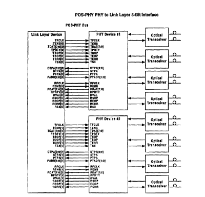
Fig. 4.2 is block diagram of two four-channel PHY
devices interfaced to a Link Layer device using 8 bit interfaces;
Fig. 5.1 shows the data structure for the 32-bit
interface;
Fig. 5.2 shows the 8-bit Interface data structure;
Fig. 6.1 are timing diagrams showing the transmit
logical timing;
Fig. 6.2 are timing diagram of the packet-level transmit
polling logical timing;
Fig. 6.3 are timing diagrams of the transmit physical
timing;
Fig. 7.1 are timing diagrams of the receive logical
timing;
Fig. 7.2 are timing diagrams of the receive logical
timing with pausing;
Fig. 7.4 are timing diagrams of the receive physical
timing;
4 StJecification Summary
4.1 Sianal Naminct Conventions
The interface where data flows from the Link Layer
device to the Physical layer device will be labeled the Transmit
Interface. The interface where data flows from the Physical Layer
device to the Link Layer device will be labeled to Receive
Interface. All signals are active high unless denoted by a
trailing "B".
SIGNAL Active high signaling.
SIGNAL B Active low signaling.
5
CA 02265346 1999-03-17
4.2 Bus Widths
POS-PHY compatible devices support an 8-bit and/or a 32-
bit data bus structure. The bus interface is point-to-point (one
output driving only one input load) and thus a 32-bit data bus
would support only one device. To support multiple lower rate
devices with point-to-point connections, an 8-bit data bus
structure is defined. Thus, each PHY device would use an 8-bit
interface reducing the total number of pins required.
To Support variable length packets, the
RMOD[1:0]/TMOD[1:0] signals are defined to specify valid bytes in
the 32-bit data bus structure. Each double-word must contain four
valid bytes of packet data until the last double-word of the
packet transfer which is marked with the end of packet REOP/TEOP
signal. This last double-word of the transfer will contain up to
four valid bytes specified by the RMOD[1:0]/TMOD[1:0] signals.
4.3 Clock Rates
POS-PHY compatible devices can support a transfer clock
rate up to 100 MHz. Some devices may support multiple rates.
Generally, devices targeted at single or multi-PHY applications,
where the aggregate PHY bit rate approached 622 Mbit/s will use
the 8-bit data bus structure with 100 MHz FIFO clock rate.
Devices targeted at applications where the aggregate PHY bit rate
approaches 2.4 Gbit/s will use the 32-bit data bus structure with
a 100 MHz FIFO clock rate.
4.4 Packet interface ~nchronization
The POS-PHY packet interface supports transmit and
receive data transfers at clock rates independent of the line bit
rate. As a result, PHY layer devices must support packet rate
decoupling using FIFOs.
6
CA 02265346 1999-03-17
To ease the interface between the Link Layer and PHY
layer devices and to support multiple PHY layer interfaces, FIFOs
are used. Control signals are provided to both the Link Layer and
PHY layer devices to allow either one to exercise flow control.
Since the bus interface is point-to-point connections, the receive
interface of the PHY device pushes data to the Link Layer device.
For the Transmit interface, the packet available status
granularity is byte-based.
In the receive direction, when the PHY layer device has
stored an end-of-packet (a complete small packet or the end of a
larger packet) or some predefined number of bytes in its receive
FIFO, it sends the in-band address followed by FIFO data to the
Link Layer device. The data on the interface bus is marked with
the valid signal (RVAL) asserted. A mufti-port PHY device with
multiple FIFOs would service each port in a round-robin fashion
when sufficient data is available in its FIFO. The Link Layer
device can pause the data flow by deasserting the enable signal
( RENB ) .
In the transmit direction, when the PHY layer device has
space for some predefined number of bytes in its transmit FIFO, it
informs the Link Layer device by asserting a transmit packet
available (TPA). The Link Layer device can then write the in-band
address followed by packet data to the PHY layer device using an
enable signal (TENB). The Link Layer device shall monitor TPA for
a high to low transition, which would indicate that the transmit
FIFO is near full (the number of bytes left in the FIFO can be
user selectable, but must be predefined), and suspend data
transfer to avoid an overflow. The Link Layer device can pause
the data flow by deasserting the enable signal (TENB).
POS-PHY defines both byte-level and packet-level
transfer control in the transmit direction. When using byte level
transfer, direct status indication must be used. In this case,
7
CA 02265346 1999-03-17
the PHY layer device provides the transmit packet available status
of the selected port (STPA) in the PHY device. As well, the PHY
layer device may provide direct access to the transmit packet
available status of all ports (DTPA[]) in the PHY device if the
number of ports is small. With packet level transfer, the Link
Layer device is able to do status polling on the transmit
direction. The Link Layer device can use the transmit port
address TADR[] to poll individual ports of the PHY device, which
all respond on a common polled (PTPA) signal.
Since the variable size nature of packets does not allow
any guarantee as to the number of bytes available, in both
transmit and receive directions, a selected PHY transmit packet
available is provided on signal STPA and a receive data valid on
signal RVAL. STPA and RVAL always reflect the status of the
selected PHY to or from which data is being transferred. RVAL
indicates if valid data is available on the receive data bus and
is defined such that data transfers can be aligned with packet
boundaries.
Physical layer port selection is performed using in-band
addressing. In the transmit direction, the Layer device selects a
PHY port by sending the address on the TDAT[] bus marked with the
TSX signal active and TENB signal inactive. All subsequent TDAT[]
bus operations marked with the TSX signal inactive and the TENB
active will be packet data for the specified port. In the receive
direction, the PHY device will specify the selected port by
sending the address on the RDAT[] bus marked with the RSX signal
active and RVAL signal inactive. All subsequent RDAT[] bus
operations marked with RSX inactive and RVAL active will be packet
data from the specified port.
Both byte-level and packet-level modes are specified in
this standard in order to support the current low density multi-
port physical layer devices and future higher density mufti-port
devices. V~hen the number of ports in the physical layer device is
8
CA 02265346 1999-03-17
limited, byte-level transfer using DTPA[] signals provides a
simpler implementation and reduces and need for addressing pins.
In this case, direct access will start to become unreasonable as
the number of ports increase. Packet-level transfer provides a
lower pin count solution using the TADR[] bus when the number of
ports is large. In-band addressing ensures the protocol remains
consistent between the two approaches. However, the final choice
left to the system designers and physical layer device and
manufacturers to select which approach best suits their desired
applications.
4.5 Application Line Rates
The numerous combinations of clock rates and bus widths
allow the Packet over SONET Interface for PHY layer devices (POS-
PHY) to support a wide range of line rates. Table 4.1 gives
examples of line rates supported by POS-PHY interfaces and the
maximum number of channels supported by the interface definitions.
Table 4.1: Interface Bit Rates
Standard Bit Rate Number of Number of
Reference (Mbit/s) PHYs PHYs
(800 Mbit/s (3.2 Gbit/s
bus) bus)
SONET STS-1 51.84 12 48
SONET STS-3
SDH STM-1 155.52 4 16
SONET STS-12
SDH STM-4 622.08 1 4
SONET STS-48
SDH STM-16 2488.32 N/A 1
4.6 PHY and Link Layer Interface Example
Figure 4.1 illustrates a conceptual example of how a
single multi-port PHY device may be interfaced to a Link Layer
device. In the example, the Link Layer device is connected to a
single package four channel PHY layer device using the 32-bit
9
CA 02265346 1999-03-17
interface. Figure 4.2 illustrates a conceptual example of how
multi-port PHY devices may be interfaced to a single Link Layer
device. The Link Layer device is connected to two four-channel
PHY layer devices using 8-bit interfaces.
In both examples, the PHY devices are using the direct
status indication signals DTPA[]. Optionally, the Link Layer
device can perform multiplexed status polling using the PTPA
signals.
5 Interface Data Structures
Packets shall be written into the transmit FIFO and read
from the receive FIFO using a defined data structure. Octets are
written in the same order they are to be transmitted or they were
received on the SONET line. Within an octet, the MSB (bit 7) is
the first bit to be transmitted. The POS-PHY specification does
not preclude the transfer of 1-byte packets. In this case, both
start of packet and end of packet signals shall be asserted
simultaneously.
For packets longer than the PHY device FIFO, the packet
must be transferred over the bus interface in sections. The
number of bytes of packet data in each section may be fixed or
variable depending on the application. In general, the Receive
Interface round-robin between receive FIFOs with fill levels
exceeding a programmable high water mark or with at least one end
of packet stored in the FIFO. The Receive Interface would end the
transfer of data when an end of a packet is transferred or when a
programmable number of bytes have been transferred. The Link
Layer device may send fixed size sections of packets on the
Transmit Interface or use the TPA signal to determine when the
FIFO reaches a full level.
Figure 5.1 illustrates the data structure for the 32-bit
bus interface. The double-word with the last byte of the packet
CA 02265346 1999-03-17
is marked with TEOP asserted and TMOD[1:0] specifying the number
of valid dates. Figure 5.2 illustrates the data structure for the
8-bit bus interface. The first byte of the packet is market with
TSOP asserted. The last byte of the packet is marked with TEOP
asserted. In all cases, the PHY address is marked with TSX
asserted.
In both illustrations, the in-band port address for
mufti-port PHY devices is not shown. The Transmit Interface would
sent the PHY port address, on the same bus as the data, marked
with the TSX signal active and the TENB signal inactive.
Subsequent data transfers on the Transmit Interface would use the
transmit FIFO selected by the in-band address. On the Receive
Interface, the PHY device reports the receive FIFO address in-band
with the RSX signal active and the RVAL signal inactive before
transferring packet data. For both cases, large packets which
exceed the FIFO size will be transferred over the POS-PHY
interface in sections with appropriate in-band addressing
prefixing each section.
The in-band address is specified in a single clock cycle
operation marked with the RSX/TSX signals. The port address is
specified by the TDAT[7:0]/RDAT[7:0] signals. The address is the
numeric value of the TDAT[7:0]/RDAT[7:0] signals where bit 0 is
the least significant bit and bit 7 is the most significant bit.
Thus, up to 256 ports may be supported by a single interface.
With a 32-bit interface, the upper 24 bits shall be ignored.
The POS-PHY specification does not define the usage of
any packet data. In particular, POS-PHY does not define any field
for error correction. Notice that if the Link Layer device uses
the PPP protocol, a Frame Check Sequence (FCS) must be processed.
If the Physical Layer device does not insert the FCS field before
transmission, these bytes should be included at the end of the
packet. If the Physical Layer device does not strip the FCS field
11
CA 02265346 1999-03-17
in the receive direction, these bytes will be included at the end
of the packet.
6 Transmit Packet Interface Description
The standard FIFO depth for POS-PHY interfaces in 256
octets. The transmit buffer shall have a programmable thresholds
defined in terms of the number of bytes available in the FIFO for
the assertion and deassertion of the transmit packet available
flags.
In this fashion, transmit latency can be managed, and
advance TPA lookahead can be achieved. This will allow a Link
Layer device to continue to burst data in, without overflowing the
transmit buffer, after TPA has been deasserted.
In the transmit direction, the PHY layer device shall
not initiate data transmission before a predefined number of bytes
or an end of packet flag has been stored in the transmit FIFO.
This capability does not affect the POS-PHY bus protocol, but is
required to avoid transmit FIFO underflow and frequent data
retransmission by the higher layers.
6.1 Transmit Signals
Table 6.1 lists the transmit side POS-PHY specification
signals. All signals are expected to be updated and sampled using
the rising edge of the transmit FIFO clock TFCLK. A fully
compatible POS-PHY Physical Layer device requires at least a 256
byte deep FIFO.
Table 6.1: Transmit Signal Descriptions
Signal Direction Function
Name
TFCLK LINK to Transmit FIFO Write Clock (TFCLK).
PHY
12
CA 02265346 1999-03-17
TFCLK is used to synchronize data
transfer transactions between the LINK
Layer device and the PHY layer device.
TFCLK may cycle at a rate up to 100
MHz.
TERR LINK to Transmit Error Indicator (TERR) signal.
PHY
TERR is used to indicate that the
current packet should be aborted. V~lhen
TERR is set high, the current packet
is
aborted. TERR should only be asserted
when TEOP is asserted.
TENB LINK to Transmit Write Enable (TENB) signal.
PHY
The TENB signal is used to control the
flow of data to the transmit FIFOs.
L~hen TENB is high, the TDAT, TMOD,
TSOP, TEOP and TERR signals are invalid
and are ignored by the PHY. The TSX
signal is valid and is processed by the
PHY when TENB is high.
V~hen TENB is low, the TDAT, TMOD, TSOP,
TEOP and TERR signals are valid and are
processed by the PHY. Also, the TSX
signal is ignored by the PHY when TENB
is low.
Signal Direction Function
Name
TDAT[31:0] LINK to Transmit Packet Data Bus (TDAT[]) bus.
PHY
The bus carries the packet octets that
are written to the selected transmit
13
CA 02265346 1999-03-17
FIFO and the in-band port address to
select and desired transmit FIFO. The
TDAT bus is considered valid only when
TENB is simultaneously asserted.
When a 32-bit interface is used, data
must be transmitted in big endian order
on TDAT[31:0]. Given the define data
structure, bit 31 is transmitted first
and bit 0 is transmitted last.
TDAT[31:0] LINK to When an 8-bit interface is used, the
Con't PHY PHY supports only TDAT[7:0].
TPRTY LINK to Transmit bus parity (TPRTY) signal.
PHY
The transmit parity (TPRTY) signal
indicates the parity calculated over
TPRTY the TDAT bus. When an 8-bit interface
LINK to is used, the PHY only supports TPRTY
PHY calculated over TDAT[7:0]. TPRTY is
considered valid only when TENB is
asserted.
When TPRTY is supported, the PHY layer
device is required to support both even
and odd parity. The PHY layer device
is required to report any parity error
to higher layers, but shall not
interfere with the transferred data.
TMOD[1:0] LINK to Transmit Word Modulo (TMOD[1:0])
PHY signal.
TMOD[1:0] indicates the number of valid
bytes of data in TDAT[31:0]. The TMOD
bus should always be all zero, except
during the last double-word transfer of
14
CA 02265346 1999-03-17
a packet on TDAT[31:0]. TnThen TEOP is
asserted, the number of valid packet
data bytes on TDAT[31:0] is specified
by TMOD [ 1 : 0 ] .
TMOD[1:0] - "00"
TDAT[31:0] valid
TMOD[1:0] - "01"
TDAT[31:8] valid
TMOD[1:0] - "10"
TDAT[31:16] valid
TMOD[1:0] - "11"
TDAT[31:24] valid
Tnlhen an 8-bit interface is used, the
TMOD[1:0] bus is not required.
TSX LINK to Transmit Start of Transfer (TSX)
PHY signal.
TSX indicates when the in-band port
address is present on the TDAT bus.
V~lhen TSX is high and TENB is high,
the
value of TDAT[7:0] is the address of
the transmit FIFO to be selected.
TSX LINK to Subsequent data transfers on the TDAT
Con't PHY bus will fill the FIFO specified by
this in-band address.
For single port PHY devices, the TSX
signal is optional as the PHY device
will ignore in-band addresses when TENB
is high.
TSX is considered valid only when TENB
is not asserted.
CA 02265346 1999-03-17
TSOP LINK to Transmit Start of Packet (TSOP) signal.
PHY
TSOP is used to delineate the packet
boundaries on the TDAT bus. When TSOP
is high, the start of the packet is
present on the TDAT bus.
TSOP is required to be present at the
beginning of every packet and is
considered valid only when TENB is
asserted.
TEOP LINK to Transmit End of Packet (TEOP) signal.
PHY
TEOP is used to delineate the packet
boundaries on the TDAT bus. When TEOP
is high, the end of the packet is
present on the TDAT bus.
When a 32-bit interface is used,
TMOD[1:0] indicates the number of valid
bytes the last double-word is composed
of when TEOP is asserted. When an 8-
bit interface is used, the last byte of
the packet is on TDAT[7:0] when TEOP is
asserted.
TEOP is required to be present at the
end of every packet and is considered
valid only when TENB is asserted.
TADR[] LINK to Transmit PHY Address (TADR[]) bus.
PHY
The TADR bus is used with the PTPA
Packet- signal to poll the transmit FIFOs
Level packet available status.
Mode
16
CA 02265346 1999-03-17
TADR[] LINK to When TADR is sampled on the rising edge
PHY of TFCLK by the PHY, the polled packet
available indication PTPA signal is
Packet- updated with the status of the port
Level specified by the TADR address on the
Mode following rising edge of TFCLK
DTPA[] PHY to Direct Transmit Packet Available
LINK (DTPA[]).
Byte-Level The DTPA bus provide direct status
Mode indication for the corresponding ports
in the PHY device.
DTPA transitions high when a predefined
(normally user programmable) minimum
number of bytes is available in its
transmit FIFO. Once high, the DTPA
signal indicates that its corresponding
transmit FIFO is not full. When DTPA
transitions low, it optionally
indicates that its transmit FIFO is
full or near full (normally user
programmable ) .
DTPA is required if byte-level transfer
mode is supported. DTPA is updated on
the rising edge of TFCLK.
STPA PHY to Selected-PHY Transmit Packet Available
LINK (STPA) Signal.
Byte-Level STPA transitions high when a
Mode predefined(normally user programmable)
minimum number of bytes are available
in the transmit FIFO specified by the
in-band address on TDAT. Once high,
17
CA 02265346 1999-03-17
STPA indicates the transmit FIFO is not
full. When STPA transitions low, it
indicates that the transmit FIFO is
full or near full (normally user
programmable).
STPA always provides status indication
for the selected port of PHY device in
order to avoid FIFO overflows while
polling is performed. The port which
STPA reports is updated on the
following rising edge of TFCLK after
the PHY address on TDAT is sampled by
the PHY device.
STPA is required if byte-level transfer
mode is supported.
STPA PHY to STPA is updated on the rising edge of
LINK TFCLK.
Byte-Level
Mode
PTPA PHY to Polled-PHY Transmit Packet Available
LINK (PTPA) signal.
Packet- PTPA transitions high when a predefined
Level (normally user programmable) minimum
Mode number of bytes are available in the
polled transmit FIFO. Once high, PTPA
indicates that the transmit FIFO is not
full. When PTPA transitions low, it
optionally indicates that the transmit
FIFO is full or near full (normally
user programmable).
18
CA 02265346 1999-03-17
PTPA allows the polling of the PHY
selected by TADR address bus. The port
which PTPA reports is updated on the
following rising edge of TFCLK after
the PHY address on TADR is sampled by
the PHY device.
PTPA is required if packet-level
transfer mode is supported. PTPA is
updated on the rising edge of TFCLK.
6.2 Examples
The following examples are not part of the requirements
definition of the POS-PHY compatibility specification. They are
only informative and provide an aid in the visualization of the
interface operation. The examples only present a limited set of
scenarios; they are not intended to imply restrictions beyond that
presented in the text of the specification. If any apparent
discrepancies exist between the examples and the text, the text
shall take precedence.
The POS-PHY transmit interface is controlled by the Link
Layer device using the TENB signal. All signals must be updated
and sampled using the rising edge of the transmit FIFO clock,
TFCLK. Figure 6.1 is an example of a multi-port PHY device with
two channels. The PHY layer device indicates that a FIFO is not
full by asserting the appropriate transmit packet available signal
DTPA. DTPA remains asserted until the transmit FIFO is almost
full. Almost full implies that the PHY layer device can accept at
most a predefined number of writes after the current write.
If DTPA is asserted and the Link Layer device is ready
to write a word, it should assert TSX, deassert TENB and present
the port address on the TDAT bus if required. Subsequent data
transfers with TENB low are treated as packet data which is
19
CA 02265346 1999-03-17
written to the selected FIFO. At any time, if the Link Layer does
not have data to write, it can deassert TENB. The TSOP and TEOP
signals must be appropriately marked at the start and end of
packets on the TDAT bus.
V~hen DTPA transitions low and it has been sampled, the
Link Layer device can write no more than a predefined number of
bytes to the selected FIFO. In this example, the predefined value
is two double-words or eight bytes. If the Link Layer device
writes more than that predefined number of words and DTPA remains
deasserted throughout, the PHY layer device should indicate an
error condition and ignore additional writes until it asserts DTPA
again.
Figure 6.2 is an example of the Link Layer device using
the polling feature of the Transmit Interface. For comparison
purposes, the direct transmit packet available signals for the
example ports are provided in the diagram. The status of a given
PHY port may be determined by setting the polling address TADR bus
to the port address. The polled transmit packet available signal
PTPA is updated with the transmit FIFO status in a pipelined
manner. The Link layer device is not restricted in its polling
order. The selected transmit packet available STPA signal allows
monitoring the selected PHY status and halting data transfer once
the FIFO is full. The PTPA signal allows polling other PHY's at
any time, including while a data transfer is in progress. The
system could be configured differently.
6.3 AC Timing
All AC Timing is from the perspective of the PHY layer
device in a PHY-LINK interface.
20
CA 02265346 1999-03-17
Table 6.2: Transmit Interface Timing
Symbol Description Min Max Units
TFCLK Frequency 100 MHz
TFCLK Duty Cycle 40 60
ts TENB Set-up time to TFCLK 3 ns
tenb
t TENB Hold time to TFCLK 0 ns
Htenb
ts TDAT[15:0] Set-up time to 3 ns
tdat
TFCLK
tH TDAT[15:0] Hold time to 0 ns
tdat
TFCLK
ts TPRTY Set-up time to TFCLK 3 ns
tprt
Y
tH TPRTY Hold time to TFCLK 0 ns
tprt
Y
ts TSOP Set-up time to TFCLK 3 ns
tsop
tH TSOP Hold time to TFCLK 0 ns
tsop
ts TEOP Set-up time to TFCLK 3 ns
teop
tH TEOP Hold time to TFCLK 0 ns
teop
ts Z'MOD Set-up time to TFCLK 3 ns
tmod
t TMOD Hold time to TFCLK 0 ns
Htmod
Symbol Description Min Max Units
ts TERR Set-up time to TFCLK 3 ns
terr
tH TERR Hold time to TFCLK 0 ns
terr
ts TSX Set-up time to TFCLK 3 ns
tsx
tH TSX Hold time to TFCLK 0 ns
tsx
TFCLK Frequency 100 MHz
TFCLK Duty Cycle 40 60
tStadr TADR[4:0] Set-up time to 3 ns
TFCLK
21
CA 02265346 1999-03-17
tH TAR[4:0] Hold time to 0 ns
tadr
TFCLK
tP TFCLK High to DTPA Valid 1 5 ns
dtpa
tP TFCLK High to STPA Valid 1 5 ns
stpa
tp TFCLK High to PTPA Valid 1 5 ns
ptpa
Notes on Transmit I/O Timing:
Note 1: When a set-up time is specified between an input and a
clock, the set-up time is the time in nanoseconds from
the 1.4 Volt point of the input to the 1.4 Volt point of
the clock.
Note 2: When a hold time is specified between an input and a
clock, the hold time is the time in nanoseconds from the
1.4 Volt point of the clock to the 1.4 Volt point of the
input.
Note 3: Output propagation delay time is the time in nanoseconds
from the 1.4 Volt point of the reference signal to the
1.4 Volt point of the output.
Note 4: Maximum output propagation delays are measured with a 30
pF load on the outputs.
7 Receive Packet Interface Description
The standard FIFO depth for POS-PHY interfaces is 256
octets. As the interface is point-to-point, the PHY device is
required to push receive packet data to the Link Layer device.
This arrangement simplifies the interface between the PHY device
and the Link Layer device. Traditional polling schemes for the
receive side are not required, saving a significant number of
pins.
The receive FIFO shall have a programmable threshold
defined in terms of the number of bytes of packet data stored in
22
CA 02265346 1999-03-17
the FIFO. A mufti-port PHY device must service each receive FIFO
with sufficient packet data to exceed the threshold or with an end
of packet. The PHY should service the required FIFOs in a round-
robin fashion. The type of round-robin algorithm will depend on
the various data rates supported by the PHY device and is outside
this specification.
The amount of packet data transferred, when servicing
the receive FIFO, is bounded by the FIFO's programmable threshold.
Thus, a transfer is limited to a maximum of 256 bytes of data (64
cycles for a 32-bit interface or 256 cycles for an 8-bit
interface) or until an end of packet is transferred to the Layer
device. At the end of a transfer, the PHY device will round-robin
to the next receive FIFO.
The PHY device should support a programmable minimum
pause of 0 or 2 clock cycles between transfers. A pause of 0
clock cycles maximizes the throughput of the interface. A pause
of 2 clock cycles allows the Layer device to cleanly pause between
transfers.
7.1 Receive Signals
Table 8.1 lists the receive side POS-PHY specification
signals. All signals are expected to be updated and sampled using
the rising edge of the receive FIFO clock, RFCLK. A fully
compatible POS-PHY Physical Layer device requires at least a 256-
byte receive FIFO.
Table 7.1: Receive Signal Descriptions
Signal Directio Function
Name n
RFCLK LINK to Receive FIFO Write Clock (RFCLK).
PHY
RFCLK is used to synchronize data
23
CA 02265346 1999-03-17
transfer transactions between the LINK
Layer device and the PHY layer device.
RFCLK may cycle at a rate up to 100
MHz.
RVAL PHY to Receive Data Valid (RVAL) signal.
LINK
RVAL indicates the validity of the
receive data signals. RVAL will
transition low when a receive FIFO is
empty or at the end of a packet.
When RVAL is high the RDAT[31:0],
RPRTY, RMOD[1:0], RSOP, REOP and RERR
signals are valid. When RVAL is low,
the RDAT[31:0], RPRTY, RMOD[1:0],
RESOP, REOP and RERR signals are
invalid and must be disregarded.
The RSX signal is valid when RVAL is
low.
RENB LINK to Receive Read Enable (RENB) signal.
PHY
The RENB signal is used to control the
flow of data from the receive FIFO's.
During data transfer, RVAL must be
monitored as it will indicate if the
RDAT[31:0], RPRTY, RMOD[1:OJ, RSOP,
REOP, RERR and RSX are valid. The
system may deassert RENB at anytime if
it is unable to accept data from the
PHY device.
V~lhen RENB is sampled low by the PHY
device, a read is performed from the
receive FIFO and the RDAT[31:0], RPRTY,
24
CA 02265346 1999-03-17
RMOD[1:0], RSOP, REOP, RERR, RSX and
RVAL signals are updated on the
following rising edge of RFCLK.
Signal Directio Function
Name n
RENB LINK to V~hen RENB is sampled low by the PHY
Con't PHY device, a read is not performed and the
RDAT[31:0], RPRTY, RMOD[1:0], RSOP,
REOP, RERR, RSX and RVAL signals will
not updated on the following rising
edge of RFCLK.
RDAT[31:0] PHY to Receive Packet Data Bus (RDAT[31:0]).
LINK
The RDAT[15:0] bus carries the packet
octets that are read from the receive
FIFO and the in-band port address of
the selected receive FIFO. RDAT[31:0]
is considered valid only when RVAL is
asserted
then a 32-bit interface is used, data
must be received in big endian order on
RDAT[31:0]. Given the defined data
structure, bit 31 is received first and
bit 0 is received last.
Tn~hen an 8-bit interface is used, the
PHY supports only RDAT[7:0].
RPRTY PHY to Receive Parity (RPRTY) signal.
LINK
The receive parity (RPRTY) signal
indicates the parity calculated over
the RDAT bus. V~hen an 8-bit interface
is used, the PHY only supports RPRTY
CA 02265346 1999-03-17
calculated over RDAT[7:0].
When RPRTY is supported, the PHY layer
device must support both odd and even
parity.
RMOD[1:0] PHY to Receive Word Modulo (RMOD) signal.
LINK
RMOD[1:0] indicates the number of valid
bytes of data in RDAT[31:0]. The RMOD
bus should always be all zero, except
during the last double-word transfer of
a packet on RDAT[31:0]. When REOP is
asserted, the number of valid packet
data bytes on RDAT[31:0] is specified
by RMOD[1:0]
RMOD[1:0] - "00"
RDAT[31:0] valid
Signal Direction Function
Name
RMOD[1:0] PHY to RMOD[1:0] ="01"
Con't LINK RDAT[31:8] valid
RMOD[1:0] ="10"
RDAT[31:16] valid
RMOD[1:0] - "11"
RDAT[31:24] valid
When an 8-bit interface is used, the
RMOD bus is not required. RMOD[1:0] is
considered valid only when RVAL is
asserted.
RSOP PHY to Receive Start of Packet (RSOP) signal.
LINK
RSOP is used to delineate the packet
boundaries on the RDAT bus. When RSOP
26
CA 02265346 1999-03-17
is high, the start of the packet is
present on the RDAT bus.
RSOP is required to be present at the
end of every packet and is considered
valid when RVAL is asserted.
REOP PHY to Receive End Of Packet (REOP) signal.
LINK
REOP is used to delineate the packet
boundaries on the RDAT bus. Tn~hen REOP
is high, the end o the packet is
present on the RDAT bus.
Tn~hen a 32-bit interface is used,
RMOD[1:0] indicates the number of valid
bytes the last double-word is composed
of when REOP is asserted. V~hen an 8-
bit interface is used, the last byte of
the packet is on RDAT[7:0] when REOP is
asserted.
REOP is required to be present at the
end of every packet and is considered
valid only when RVAL is asserted.
RERR PHY to Receive error indicator (RERR) signal.
LINK
RERR is used to indicate that the
current packet is aborted and should be
discarded. RERR shall only be asserted
when REOP is asserted.
Signal Direction Function
Name
RERR PHY to Conditions that can cause RERR to be
Con't LINK set may be, but are not limited to,
FIFO overflow, abort sequence detection
27
CA 02265346 1999-03-17
and FCS error.
RERR is considered valid only when RVAL
is asserted.
RSX PHY to Receive Start of Transfer (RSX) signal.
LINK
RSX indicates when the in-band port
address is present on the RDAT bus.
V~lhen RSX is high and RVAL is low, the
value of TDAT[7:0] is the address of
the receive FIFO to be selected by the
PHY. Subsequent data transfers on the
RDAT bus will be from the FIFO
specified by this in-band address.
For single port PHY devices, the RSX
signal is optional as the PHY device
will not need to generate in-band
addresses.
RSX is considered valid only when RVAL
is not asserted.
7.2 Examples
The following examples are not part of the requirement
definition of the POS-PHY compatibility specification. They are
only informative and provide an aid in the visualization of the
interface operation. The examples only present a limited set of
scenarios; they are not intended to imply restrictions beyond that
presented in the text of the specification. If any apparent
discrepancies exist between the examples and the text, the text
shall take precedence.
28
CA 02265346 1999-03-17
The POS-PHY Receive Interface is controlled by the Link
Layer device using the RENB signal. All signals must be updated
and sampled using the rising edge of the receive FIFO clock. The
RDAT bus, RPRTY, RMOD, RSOP, REOP and RERR signals are valid in
cycles for which RVAL is high and RENB was low in the previous
cycle. When transferring data, RVAL is asserted and remains high
until the internal FIFO of the PHY layer device is empty or an end
of packet is transferred. The RSX signal is valid in the cycle
for which RVAL is low and RENB was low in the previous cycle.
Figure 7.1 is an example of a multi-port PHY device with
at least two channels. The PHY informs the Link Layer device of
the port address of the selected FIFO by asserting RSX with the
port address on the RDAT bus. The Link Layer may pause the
Receive Interface at any time by deasserting the RENB signal.
When the selected FIFO is empty, RVAL is deasserted. In this
example, the RVAL is reasserted, without changing the selected
FIFO, transferring the last section of the packet. The end of the
packet is indicated with the REOP signal. Thus, the next
subsequent FIFO transfer for this port would be the start of the
next packet. If an error occurred during the reception of the
packet, the RERR would be asserted with REOP. Since another
port's FIFO has sufficient data to initial a bus transfer, RSX is
again asserted with the port address. In this case, an
intermediate section of the packet is being transferred.
Figure 7.2 is an example of a multi-port PHY configured
to gap transfers for two clock cycles. The first transfer is a
complete 3-byte packet and the second transfer is the end of a 36-
byte packet. The pause allows the Link Layer device to cleanly
halt the transfer of data between transfers. In order to handle
an unexpected end of packet, the Link Layer device may deassert
the RENB signal when its samples the REOP active. As shown in the
diagram, the Link Layer device pauses the PHY device on the in-
band address for two clock cycles.
29
CA 02265346 1999-03-17
7.3 AC Timina
All AC Timing is from the perspective of the PHY layer
device in a PHY-LINK interface.
Table 7.3: Receive Interface Timing
Symbol Description Min Max Unit
s
RFCLK Frequency 100 MHz
RFCLK Duty Cycle 40 60
tsrenb RENB set-up time to RFCLK 3 ns
tHrenb RENB hold time to RFCLK 0 ns
tPrdat RFCLK High to RDAT Valid 1 5 ns
tPrprt RFCLK High to RPRTY Valid 1 5 ns
Y
tPrsop RFCLK High to RSOP Valid 1 5 ns
tPreop RFCLK High to REOP Valid 1 5 ns
tPrmod RFCLK High to RMOD Valid 1 5 ns
tPrerr RFCLK High to RERR Valid 1 5 ns
tPrval RFCLK High to RVAL Valid 1 5 ns
tPrsx RFCLK High to RSX Valid 1 5 ns
Notes on Receive I/O Timing:
Note 1: V~hen a set-up time is specified between an input and a
clock, the set-up time is the time in nanoseconds from
the 1.4 Volt point of the input to the 1.4 Volt point of
the clock.
Note 2: V~hen a hold time is specified between an input and a
clock, the hold time is the time in nanoseconds from the
CA 02265346 1999-03-17
1.4 Volt point of the clock to the 1.4 Volt point of the
input.
Note 3: Output propagation delay time is the time in nanoseconds
from the 1.4 Volt point of the reference signal to the
1.4 Volt point of the output.
Note 4: Maximum output propagation delays are measured with a 30
pF load on the outputs.
Accordingly, while this invention has been described
with reference to illustrative embodiments, this description is
not intended to be construed in a limiting sense. Various
modifications of the illustrative embodiments, as well as other
embodiments of the invention, will be apparent to persons skilled
in the art upon reference to this description. It is therefore
contemplated that the appended claims will cover any such
modifications or embodiments as fall within the true scope of the
invention.
31