Note: Descriptions are shown in the official language in which they were submitted.
CA 02266119 1999-03-12
TITLE
Touch Screen Based Upon Topological Mapping
With Resistance Framing Design
INTRODUCTION
Since their introduction in the early 1970s, touch screens
have afforded attractive alternatives to keyboards for certain
computer applications. In many situations the keyboard and mouse are
eliminated, because the touch screen provides the user with a much
easier access to the computer. As a consequence, the market has
grown to a substantial size, and a continued rapid growth is
anticipated. However, current touch screens are difficult to
produce, which creates a price barrier limiting growth into many new
areas, such as education.
In this disclosure, a new concept is discussed that
virtually eliminates design constraints and provides more freedom for
the configuration of touch screens. Examples are given to illustrate
this new freedom in design parameters. These design concepts provide
a basis for producing touch screens at a much lower cost, without
sacrificing quality. Furthermore, the creation of new designs for
66'7282.1
::ODMA\PCDOCS\DpCg\667282\ I
CA 02266119 1999-03-12
special sensor size, shape, or elect:rical characteristics is greatly
simplified with the concept described herein and reduces research and
development costs.
BACKGROUND OF TIiE INVENTION
A substantial portion of the touch screens produced today
are based on the measurement of electrical potentials on substrates
that are made of a transparent medium such as glass, coated with an
electrically conductive material. Uniform electrical fields must be
maintained on the substrate, and these are applied sequentially in
the x- and y-directions.
In other words, equally spaced equipotential lines are
generated orthogonally in a timed sequence. A voltage (or
equivalently, a current related to the local potential of the touch
point) measured when the field is in the x-direction is directly
proportional to the distance a:Long the x coordinate and is
independent of the y coordinate. Conversely, a voltage measured when
the field is in the y-direction is directly proportional to the
distance along the y coordinate and. is independent of the value of
X.
According to present designs, resistive touch screens are
often mounted on LCD or CRT displays, but perhaps most commonly on
CRTs used as computer monitors to use as data input devices. As
shown in Figure 6 a typical monitor 10 will comprise a back case 11
into which is set the CRT. A glass panel 12 with a uniform resistive
656095.2 2
::ODMA\PCDOC S\DOCS\667282\ 1
CA 02266119 1999-03-12
coating 15 (shown in Figure 7) suc:h as ITO (indium tin oxide) is
placed over the face 14 CRT 13. A polyester cover sheet is tightly
suspended over the top of the glass panel, preferably separated from
it by small transparent insulating dots 16 as described in Hurst,
U.S. Patent No. 3,911,215.
The cover sheet 17 has a conductive coating on the inside and a hard
durable coating 18 on the outer side. A more detailed view of the
layers of the touch screen is shown in Figure 7, with a bezel 19.
A simple computer or controller 20 (shown in Figure 8) is
used to alternate a voltage across the resistive surface of the glass
in the X and Y directions. When a touch on the cover sheet causes
the inner conductive coating to make electrical contact with the
resistive coating on the glass, an electrical circuit connected to
the controller digitizes these voltages or equipotentials and
transmits them to the associated main computer 21 for processing. As
shown in Figures 8A and 8B, the controller 20 may be mounted internal
to the monitor 10 or in a slot within the associated main computer
21.
In practice, the implementation of these concepts, as
disclosed in the Paterit of Hurst (U.S. Patent 3,798,370, March, 1974)
leads to the production of touch screens of excellent quality. Yet
production costs are high, because of three factors:
656095.2 3
::ODMA\PCDOCS\D0CS\667282\ I
CA 02266119 1999-03-12
1) The substrate must have very uniform conductivity. Conductive
materials are applied to a substrate (usually glass) in
elaborate coating chambers. TAThen a large substrate is being
prepared, the chamber must be still larger, and even then,
several sources must be used to cover the substrate uniformly.
Some of these coated substrates do not meet specifications and
have to be rejected.
2) A resistor divider network must be added to maintain straight
equipotentials by eliminating edge effects associated with the
field switching matrix. This has independent quality demands
that further add to production costs and increase rejection
rates.
3) Finally, rigorous testing must be done on the substrate itself
and on each completed screen. T'hese statistical quality-control
tests are expensive and are directly associated with the problem
of maintaining accurate equipotentials.
Currently, design changes requires considerable retooling.
However, retooling costs and delays are considerably reduced by using
the new concepts in the present in=vention. These concepts, to be
explained, will reduce all of the cost factors and, at the same time,
provide much more flexibility in the design of sensors of the
required shape, size, and electrical specifications.
656095.2 4
::ODMA\PCDOCS\DOCS\667282\ i
CA 02266119 1999-03-12
SZTMMARY OF THE INVENTION
It is therefore a purpose of the invention to provide
improved touch screen production by enhancing screen yield through
an inherent tolerance for individual and lot variances. It is a
further object of the invention to permit simplified manufacture
requirements for touch screens including less-demanding conductive-
coating application; fewer and much simpler electrodes -- only four,
for example, or even a simple resistance framing design; with no
divider resistors required. It is yet another purpose of the
invention to provide compatibility with current manufacture of
analog-to-digital electronics, and calibration/testing procedures.
It is yet another object of the invention to permit manufacture at
low additional cost, more than offset by savings in screen
manufacture. It is another purpose of the invention to permit
liberated design of touch screens with changes readily implemented
to accommodate new screen configurations.
BRIEF DESCRIPTION OF THE DRAWINGS
Figure 1A shows a contour plot of theoretical
equipotentials in the y-direction on a touch screen sensor according
to the present invention with four electrodes and non-linear
equipotential lines;
Figure iB shows a contour plot of theoretical
equipotentials in the x-direction ori a touch screen sensor according
656095.2 5
:: O DMA\PCDOCS\DOCS\667282\ 1
CA 02266119 1999-03-12
to the present invention with four electrodes and non-linear
equipotential lines;
Figure 2 shows a three-di'mensional plot of the potential
distribution in the sensor with the configuration shown in Figures
lA and B;
Figure 3 shows a plot of current flow lines in a sensor
having four electrodes at the corners.
Figure 4 illustrates a contour plot of theoretical
equipotentials in a sensor with non-uniform conductivity to simulate
conditions that might result from vacuum evaporation and deposits of
the conductive substance.
Figure 5A illustrates the location of cells by the process
of border mapping in the usual case.
Figure 5B illustrates the special condition when the severe
bulging of an equipotential causes a given equipotential to intersect
a rectangular function box at four points;
Figure 6 illustrates a typical monitor with touch screen
input device;
Figure 7 illustrates a detailed view of the layers of a
resistive touch screen;
Figure 8A shows a representative touch screen monitor with
an internal controller;
Figure 8B shows a represer.Ltative touch screen monitor with
an external controller; and
656095.2 6
::ODMA\PCDOCS\DOCS\667282\ 1
CA 02266119 1999-03-12
Figure 9 illustrates a contour plot of theoretical
equipotentials in a rectangular se:nsor with an electrode in the
center of each side.
Figure 10A is a representation of a set of equipotentials
in a picture frame sensor configuration according to the present
invention. The width of the frame is taken to be one unit in a 20X28
sensor and its conductivity is 1000 times that of the central sensor
area. The electrodes at the four corners are L-shaped and each
segment of the L is taken to have unit length. The applied potential
of one unit is assumed between the top pair and the bottom pair of
electrodes.
Figure lOB is a depiction of the sensor counterpart of
figure 10A, however, equipotentials for unit potential applied
between the left pair and the right pair of electrodes.
Figure 11A shows equipotentials in the same sensor
configuration of Figure 10A except that the frame is taken to have
a thickness of only 0.1 units, its conductivity is taken as 10,000
times that of the central area, and the L-electrodes are chosen to
have length equal to that of the frame width.
Figure 11B is a depiction of the sensor configuration from
Figure 11A, however, the applied potential is taken in the x-
direction between the left and right pairs of electrodes.
Figure 12A shows equipotentials in the same sensor
configuration as in Figure 10A except that a circular region of 5
656095.2 7
::ODMA\PCDOCS\DOCS\667282\ l
CA 02266119 1999-03-12
units radius located in the center of the sensor is taken to have
conductivity of half that of the sensor. The potential is applied
in the y-direction between the top and bottom pairs of electrodes.
Figure 12B shows the same sensor as in 12A except that the
potential difference is applied in the x-direction between the left
and right pairs of electrodes.
Figure 13A shows equipotentials in the same sensor
configuration as in Figure lOB except that a circular region of 5
units radius located in the center of the sensor if taken to have
conductivity of twice that of the sensor. The potential is applied
in the x-direction between the left and right pairs of electrodes.
Figure 13B shows the same sensor as in 13A except that the
potential difference is applied in the y-direction between the top
and bottom pairs of electrodes.
Figure 14A is the same sensor configuration as figure 10A
except that the conductivity of the frame is taken to be only 10
times that of the sensor center with a one unit wide frame in the
standard 20X28 configuration. The electrodes are L-shaped with unit
length segments. With this lower conductivity there is some non-
uniformity.
Figure 14B shows equipoter.itials for the same configuration
as in 14A, but with circular electrodes. Note that with this
combination of frame thickness andl conductivity, there is little
656095.2 8
::ODMA\PCDOCS\DOCS\667282\ I
CA 02266119 1999-03-12
difference in the equipotentials whether the corner electrodes are
circular or L-shaped.
Figure 15A shows equipotentials in the original uniform
conductivity sensor of figure la with 12 flat, unit length electrodes
distributed uniformly around the perimeter. L-shaped electrodes are
at the corners, while electrodes on the sides are assumed to be held
at potentials depending linearly on the distance from the corner pair
that establish the potential difference.
Figure 15B shows equipotentials on the same sensor as in
figure 15A except that the applied potential is in the x-direction
between the left and right sets of: electrodes. In this case the
equipotentials are more nearly parallel except very near the
electrodes and are a definite improvement over the equipotentials of
Figure lA and iB.
Figure 16 shows equipoten'tials for the same configuration
as shown in Figure 14A, except that the conductivity of the frame is
100 times that of the sensor center. The equipotentials are more
nearly parallel, easily handled using electronic controllers and data
processing, as indicated in the text, but by increasing the
conductivity still further by a factor of 10, as in Figure 10,
excellent parallelism is achieved.
Figure 17 shows equipoter.itials for a 20X28 picture frame
screen with the perimeter frame regions 2 units wide, with L-
electrodes 2 units wide and for conductivity of the frame 500 times
656095.2 9
::O DMA\PC DOCS\DOCS\667282\ l
CA 02266119 1999-03-12
that of the sensor center, in accorci with the idea that the product
of conductivity and frame width should remain constant.
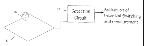
Figure 18 shows a simple schematic diagram of a touchdown
detector that may be advantageously employed to reduce power
consumption.
DETAILED DESCRIPTION OF THE INVENTION
For the purpose of describing the invention, it is best to
define a space in terms of electric equipotentials. In principle,
coordinate mapping can be obtained using any set of electrodes that
generates monotonic equipotentials. In terms of topology, this means
that the space must be defined with equipotentials that are
topologically equivalent to the Cartesian space to be mapped to. For
a surface, lines drawn at the same potential in the space between the
opposing sets of electrodes are called equipotential lines. Full
two-dimensional mapping on that suirface can be achieved using two
sets of monotonic equipotentials in two different directions. The
potential lines need not be straight. or uniform, but the key idea is
that any point on that surface must have a unique value for the pair
of potentials at that point. In topology, this uniqueness is
expressed in terms of "topological equivalence;" two surfaces are
topologically equivalent when all points on one surface can be mapped
to unique points on the other surface.
Consider, as diagramed in Figures 1A and 1B, a two-
dimensional surface 30 that is slightly conductive (or, if you
656095.2 10
::ODMA\PCDOCS\DOCS\667282\ 1
CA 02266119 1999-03-12
prefer, resistive). A very simple geometry with electrodes 31
attached at each of the four corner's can be used to illustrate the
basic idea. The exact solution for the potential distributions also
provided by Laplace's equation as described below. The usual
Cartesian space with x-y coordinates can be mapped by two sets of
equipotential lines. One of these sets is obtained when a source of
electrical potential such as a battery is applied so as to produce
an electrical field generally in the y-direction; equipotentials 32
will run generally in the x-direction (Figure lA). When the battery
is switched to produce a field generally in the x-direction,
equipotentials will run generally in the y-direction (Figure 1B).
The word "generally" is used to stress that nowhere are we assuming
uniform fields or equipotentials that run parallel to the x- or y-
axes. There is distortion (i.e., the equipotentials are not evenly
spaced nor are they parallel to the x-and y-axes), since the
electrodes are not at all designed to produce uniform fields, and
because the electrical conductivity need not be uniform. Obviously,
one set of equipotentials need not be orthogonal to a second set when
the voltage source is switched from one direction to another.
The notation V(X,y) is used to mean an equipotential when
the voltage supply is connected in the x-direction (Figure 1B), and
the lower-case y is shown to indicate that the equipotential also
depends on y, due to the distortion. Similarly, V(Y,x) is used for
656095.2 11
::ODMA\PCDOCS\DOCS\667282\ 1
CA 02266119 1999-03-12
the equipotentials when the voltage supply is connected in the y-
direction (Figure 1A). Near the center of the screen, there is
little or no distortion and it is possible to approximate V(X,y) with
V(X), i.e., the equipotential in x:is essentially independent of y.
Of course, a similar statement cou:Ld be made of the complementary
case, V(Y,x). Near the edges of the sensor there is appreciable
distortion, which is permitted here, but would be fatal to the
performance of conventional touch screens that require uniform
potential distributions.
Because of this interdependence of potential upon both x
and y, a single potential measurement cannot uniquely specify either
x or y. Consequently, it is no longer possible to measure x
independent of y, and y independent, of x. This must be given up in
the present considerations; however, the pair of potentials
[V (X, y) , V(Y, x) ] uniquely transforms to a point P(x,y) in the
Cartesian space, under certain conditions. It is this uniqueness
that is important to the invention. With this uniqueness, operations
can be found that will map the pair [V (X, y) , V(Y, x) ] to a unique point
P(x,y) in Cartesian space.
Certain conditions are required for this uniqueness. One
condition is that the field (i.e., potential gradient or change in
potential) be continuous over the entire area in each of the
directions of application. A related condition is that the field has
no singularities over an appreciable area of the substrate. These
656095.2 12
::ODMA\PCDOCS\DOCS\667282\ I
CA 02266119 1999-03-12
field conditions imply that the equipotentials must increase
continuously in the direction of the applied potential. These
conditions, in turn, impose some practical conditions on the
substrate, which is often prepared by vapor deposition. The coating
need not be uniform, but it must be continuous without isolated areas
of no conductivity. Further, the coating must not be so heavy in the
other areas so as to substantially "short" them. Both of these
conditions are much more easily Satisfied than is required for
present touch screens. There is another condition related to how
much variation in the field we can allow in practice. A weak-field
region presents a problem for precisely determining the sensed point.
Finally, in order to make precise determinations of the Cartesian
coordinates, the equipotentials must substantially intersect over all
of the working area of the screen.
Many designs with alternative electrode placement can be
conceived. However, one of the simplest designs is that shown in
Figures 1A and 1B. This configuration consists of four electrodes in
the form of quarter-circles located at the corners of a rectangular,
uniformly conducting sensor. Figure: 1A represents equipotentials in
a rectangular sensor when a unit potential difference is applied in
the y-direction between the top and bottom electrode pairs. Figure
1B shows corresponding data wher.L the potential difference is
maintained in the x-direction between the side pairs of electrodes.
656095.2 13
::O DMA\PCDOCS\DOC S\667282\ 1
CA 02266119 1999-03-12
It should be noted that although the potential near each
electrode departs from uniformity in both figures, a pair of
potential readings (corresponding to the two different directions of
applied potential) at an arbitrary point on the sensor will clearly
yield a unique answer, over most of the sensor area. The system of
electronic interpretation visualized.here allows mapping of these two
potential readings to the coordinates of the point at which the
measurements were made. Note that the equipotentials of one set need
not be orthogonal to those of a second set when the voltage source
is switched from one direction to ainother.
As discussed above, certain conditions are required for the
unique mapping of the pair [V(X,y), V(Y,x)] to a point in Cartesian
space. The most important condit_Lon is that there must be some
crossing of the complementary equipotentials, as discussed in the
introduction.
In practice, there is a finite precision given by the
electronic analog and digital noiLse. Therefore, the lines of
equipotential become bands within which the change in potential
measured cannot be discerned. For polarization in both directions,
the overlap area of bands gives ail uncertainty in the coordinate
mapping.
MAPPING OPTIONS
Some, but not all, applications of touch screens based on
the potential pairs will require mapping to a Cartesian coordinate
656095.2 14
::ODMA\PCDOCS\DOCS\667282\ 1
CA 02266119 1999-03-12
system. There are several possibilities to fit any number of
applications.
Direct address. In principle it is possible to communicate
with an attached computer or cash register without ever leaving the
potential-pair space. However, this would not appeal to users who
have been brought up in a Cartesian world, and as "Cartesianites"
would feel uncomfortable working with, for example, curved menu
boxes. This would be the least den:ianding, since little technology
would be required for implementation. This possibility is given
mainly to set the stage for more serious mapping options.
Complete mapping. This term applies to cases where it is
elected to store each point in a built-in table (i.e., memory for
each pixel required). This option would use an auxiliary mapping
device with enough memory to define the required number of pixels in
the x-y plane. The device would store a large array of pre-defined
x,y points corresponding to the field of points in the
[V(X,y),V(Y,x)] space, so that a"look-up" table (LUT) could be used
in the mapping. In this case, the LUT would be a device or process
whereby a potential pair, [V(X,y),V(Y,x)], in suitable digital form
would be used to locate in a two-dimiensional table the corresponding
real-space coordinate pair, (x,y), also in digital form. Resolutions
of 128x128 to 1024x1024 would require 32Kbytes to 4Mbytes of LUT
memory, respectively. This option is becoming increasingly
attractive as computer chips drop in price.
656095.2 15
::O DMA\PCDOCS\DOCS\667282\ 1
CA 02266119 1999-03-12
Interpolative mappincr. Iri practice, intermediate points
between two tabulated points can be determined by interpolation.
This option would store calibration points and fill in all
intermediate points by interpolation. In a sense, interpolative
mapping can be regarded as a processor-based method of achieving
complete mapping that uses less memory than a complete LUT. In this
connection, a mathematical solution of the boundary-value problem
would be very powerful, especially if the solution is able to adjust
to substrate irregularities. For instance, a math chip or programmed
processor could be used to solve a partial differential equation
known as Laplace's equation, and the interpolation between points
could be based on this solution. It is anticipated that the solution
to the partial differential equation would automatically take into
account non-uniformity in the substrate, and thus serve as an
accurate interpolation independent of substrate characteristics.
Even simpler would be a modest resolution LUT (say, 256 x
256 points) and a Iinear-interpolation algorithm. For example, a
pair of 12-bit (4096) potential readings could be trimmed to 8 bits
(256) before interpretation by the LUT. The 4-bit remainders would
then be used for linear interpolation between adjacent points in the
LUT. The resultant answer would yield complete mapping at 12-bit
(4096) resolution. The code required for this is very small, so that
even a modest-sized LUT with a simple programmed processor would be
used.
656095.2 16
::OD MA\P CDOCS\DOC,S\667282\ l
CA 02266119 1999-03-12
Boundary mapping. In this case, an active area, such as
a menu box, can be defined without complete, one-to-one mapping. For
instance, straight-sided boxes (or other shapes) could be defined by
their boundaries, stored as potential pairs. A simple logic could
be employed to locate the potential pair, [V(X,y),V(Y,x)], within or
outside the boxes. Typically a lim:i.ted number of boxes are used in
menu selection, so that the memory required would be greatly reduced
from complete mapping. Perhaps a small LUT could be used that define
areas where this boundary analysis is to be made.
BOUNDARY MAPPING OF MENU BOXES
A common end-use of the touch screen is the so-called menu
application. Choices are made by the user simply by touching menu
items typically enclosed by rectangiular boundaries. In this case it
is possible to map only around the perimeter (boundary) of the box.
Define the points around the perimeter of the rectangular box, in
terms of the pairs !V(x,y),V(Y,x)] and use an electronic test to
determine if the point in the measurement space is within the
rectangular box.
Expanding on the discussion of this option, Figures 5A and
SB illustrate the definition of a rectangular box 40 by means of the
measured coordinates based on equipotential pairs. This illustration
makes it clear that any pair of potentials measured within the box
656095.2 17
::ODMA\PCDOCS\DOCS\667282\ i
CA 02266119 1999-03-12
so defined can be assigned uniquely to the box defined by Cartesian
coordinates.
An electronic test determ:ines if the measurement space is
within the selection area. In the box illustration of Figure 5A,
note that its entire perimeter could.be defined with as few as eight
measurements of the potential pairs at the indicated Cartesian
points. From the three measurements on each edge, a polynomial of,
for example, three terms (e.g., a+bz+cz2) could be fitted to both of
the measured members for each of the potential pairs, giving two sets
of coefficients in the polynomial. Thus, for the four sides only
eight sets of these coefficients (a total of 24 coefficients) are
needed to completely specify (with good accuracy) the perimeter of
the box. Assuming that each coefficient is an eight-bit byte, only
192 bits, or 24 bytes, of storage space is required.
Having defined the box, where the measurement space is now
made to conform to the rectangular Cartesian space, a test can be
described to see if the measured poirit is within the Cartesian space.
Imagine, as in Figure 5A, that either of the two potentials measured
at a particular point, P, is on an i=_quipotential 32 that intersects
the box at two places. Neither of the two equipotentials 32 alone
will select a particular Cartesian box, as shown. However, the pair
of equipotentials 32 will intersect only at one point and therefore
in a particular box. Thus, a boundary analysis, by the procedure
656095.2 18
::ODMA\PC DOCS\DOCS\667282\ 1
CA 02266119 1999-03-12
that searches all boxes and finds the four points on the perimeter
of a box, will select that particular box. A box is selected by
finding just two potentials on its perimeter, provided that the two
potentials are complements; i.e., one value belongs to V(X,y) and one
to V(Y,x). With modern data processing, this search procedure is
routine. For instance, the two potentials measured could first be
stored in a register until the boundary analysis described above is
completed.
In the case of severe bulging of an equipotential 32 shown
in Figure 5B, it is possible that a given equipotential will
intersect a box at four places rather than two. This could produce
some ambiguity in assigning a pair af potentials to a box. However,
this can be avoided by applying a special test. In the above
paragraph, a regular test is described that will be by far more
common than the special test. In the special test a concept of
complementary potentials is employeci. At every point in the working
area, there is an intersection of two equipotentials. The discussion
will focus on just one of these, and the other will be considered its
complement. At each of the places where one equipotential 32 crosses
the boundary of a box 40 there will be a value for the corresponding
complement. The special test looks at the complement in potential
actually measured and tests to see that its magnitude lies
intermediate to the complements created at the boundary crossings.
656095.2 19
::O DMA\PC DOCS\DOCS\667282\ i
CA 02266119 1999-03-12
In the case where there are four crossings this test could be applied
and in three regions of the sensor, as illustrated in Figure 5B.
The special test just ciescribed removes any possible
ambiguity due to four crossings o:E one equipotential on the box
boundary. However, a more attractive alternative could be simply to
electronically abort any touch that results in four crossings. This
would create very small inactive areas, which would go unnoticed in
most applications. This test procedure is not restricted to
rectangles. For instance, the control "box" could be a circle or an
arbitrary enclosure. However, for complex figures, boundaries or
perimeters, definition becomes correspondingly more complex.
And, of course, the special test can be avoided altogether
by using the concept of "cells" that are small enough to eliminate
multiple crossings. An extra cell can be added wherever there are
multiple boundary crossings, guided by principles of symmetry. For
instance, in Figure 5B, the box containing Region 2 could be divided
into two cells by the addition of a horizontal boundary line. A menu
box would then be configured from any number of cells. Reasonable
sensor design to avoid excessive curvature of equipotential lines
would greatly reduce the number of cells needed, perhaps to one per
menu box.
MATHEMATICAL SOLUTIONS
The electrical potential distribution of a conducting
sheet is determined by the configuration of electrodes, the
656095.2 20
::ODMA\PCDOCS\DOCS\667282\ I
CA 02266119 1999-03-12
potentials applied to them, and the: conductivity, S, of the sheet.
In general S= S(x,y) is a function of position. We further assume
that the conductivity is isotropic (but not necessarily uniform).
Then if V(x,y) is the electric potential at (x,y), the resulting
current j(x,y) is given by:
j(x,y) = -8(x,Y,1PV(x.Y), (Al)
We assume that charge cannot accumulate at any point, hence:
V. j (x,y) = 0, (A2 )
and from substitution of Eq. (Al) into Eq. (A2) :
V. !8(x,y) PV(x,y)1 = 0 (A3)
This is the equation that is used to solve for V(x,y),
subject to a boundary condition for a given distribution of applied
electrical potential on the electrodes. The electrodes may be of any
shape, including circular spots 31 as shown in the illustrations of
Figure 1A and Figure iB. In that case, the sheet is 20 x 28 cm with
1-cm radius circular electrodes centered on the four corners of sheet
with uniform conductivity.
The method of images is often used to satisfy equation A3
for a given set of electrodes and :boundaries. It is based on the
fact that, away from actual sources, and for 8 equal to constant (k)
656095.2 21
::ODMA\PCDOCS\DOCS\667282\ I
CA 02266119 1999-03-12
in an infinite medium, equation A3 becomes Laplace's equation and is
exactly satisfied; thus one may be able to distribute sources outside
of the physical region in such a way that the boundary conditions are
satisfied and that requisite real currents are well-represented.
Many such solutions have been found in the mathematical theory of
electrostatics. In preliminary testing an infinite rectangular grid
of infinitely long current sources and sinks has been constructed to
approximate the potential in a rectangular sensor with circular
electrodes. The boundary conditions at the edges of the sensor,
viz., that electric lines of force shall be parallel with the
boundary, are well satisfied in this model.
Alternatively, equation A3 may be solved directly by
numerical means in order to represent real sensors with complicated
boundaries and electrodes. Various techniques for solving equation
A3 have been developed extensively over many years. For example, the
conformal transformation method is useful for problems in two
dimensions with boundaries that are fairly simple. A brief
discussion is given in "Mathematical Methods of Physics" by J.
Mathews and R. L. Walker, Benjamin, IJY, 1964. Relaxation methods are
more generally useful for complex creometries and have been applied
to the numerical solution of many different problems in physics and
engineering. A standard reference is "Relaxation Methods in
Theoretical Physics" by R.V. Southwe:ll, 1946, while more recent work
that is designed to take advantage of the capabilities of modern
656095.2 22
::ODMA\PCDOCS\DOCS\667282\ I
CA 02266119 1999-03-12
computers is described, e.g., in "The Finite Element Method" by O.C.
Zienkiewicz and R.L. Taylor, McGraw Hill, 1987, and in "The Finite
Element Method in Electromagnetics" by J.-M. Jin, Wiley, 1993.
Figures 2 and 3 show alternative ways of displaying the
configuration of Figure 1A: three-dimensional potential and current
distributions, respectively. These are useful to further understand
the distorted space of non-uniform potentials that occurs with the
simplified electrode configuration.
Experiments approximating this model were done by making
electrodes in the form of discs of 7-mm diameter (using highly
conductive nickel paint) applied to electrically conductive paper.
These intuitively designed experimerits gave excellent results. Even
for a line drawn less than 1 cm from the two electrodes (spaced about
cm apart) on the left of the figure, there was less than a factor
15 of two variation in the electrical potentials as read with a digital
voltmeter of high input impedance. At 2 cm from the electrodes this
factor was reduced to 1.5 and at a distance of 4 cm, this factor was
about 1.25. At the center of the 28-cm conductive paper this factor
was about 1Ø Thus, while the equipotentials are far from vertical
20 (along the y-axis) there is no region of the sensor that deviates
from norm by more than a factor of two. There were no "insensitive"
regions where a change in position would give essentially the same
potentials.
Another simple design was tested utilizing a single
656095.2 23
::O DMA\PCDOCS\DOC S\667282\ I
CA 02266119 1999-03-12
electrode at the center of the four edges of a rectangle. However,
as shown in Figure 9, actual potential measurements on this design
revealed regions near each of the corners that were "insensitive" and
therefore would not be a good touch screen design. This effect could
be anticipated simply by looking at the equipotentials in the
vicinity of the corners. In these regions the equipotentials spread
out indicating that the electrical fields are weak in these regions
in comparison with the central region.
In some designs the equipotential pair V(X,y) and V(Y,x)
may not cross sufficiently for the determination of the point P(x,y) .
This tends to become a problem in the vicinity of the electrodes as
Figures 1A and 1B show. Variation of electrode design can be used
to solve this problem.
The examples illustrate an important point: it is quite
easy to arrive at sensor designs where nearly all points on the
planar surface can be characterized. by a unique pair of potentials
(V(X,y),V(Y,x)] and where the fields vary by less than a factor of
two, so that all regions of the sensor can be regarded as responsive.
Of course, these examples are far from exhaustive; the designs could
be combined to have eight electrodes. The electrodes could be
rectangles instead of circles, etc. There is great flexibility
because we have liberated our desigr.ifrom the requirement of uniform
electrical fields. Non-uniformity in the electrical fields may be
due both to electrode designs and non-uniform coatings of the screen.
656095.2 24,
::O DMA\PCDOCS\DOCS \667282\ i
CA 02266119 1999-03-12
If the conducting material has a non-uniform thickness, the
potential will be affected by a non-constant S(x,y) in Eq. (A3). For
example, if 8(x,y) _ {1+0.01!(x-10)Z+(y-142)21)-', then the
conductivity at the center of the sheet is twice that on a circle of
radius 10 cm and centered at the center of the sheet. Such a
conductivity function might represent that generated in vacuum
deposition of conducting material from a single source located over
the center of the substrate. Figure 4 shows a contour plot of the
equipotentials for the same configuration as in Figure 1A, but with
the above spatially varying conductivity.
RESISTANCE FRAMING DESIGN
The electrode configurations disclosed in Figures 1-9 are
very simple (for example a portion of a small circle at the four
corners of a resistive sheet). These are generally satisfactory
sensor designs when used under the iumbrella of the topology mapping
concepts. Over almost the entire a:rea of the resistive surface, an
equipotential pair, generated by the switching action of the
controller, can be transformed to a unique Cartesian coordinate with
suitable accuracy. However, in the vicinity of these electrodes
there remains a problem of uniqueness; that is, equipotential pairs
cannot be transformed to unique Cartesian coordinates. This results
in regions around the electrodes that are not suitable as working
656095.2 25
::ODMA\PCDOCS\DOCS\667282\ I
CA 02266119 1999-03-12
area, an undesirable effect in today's highly competitive touch
screen market.
It is helpful to elaborate on the uniqueness problem for
the discussion that follows. If a circular electrode is polarized
in the x-direction, equipotentials near the circle are circular and
if polarized in the y-direction, these equipotentials are also
circular. This means that in this small region near the electrodes
each pair of equipotentials created. at a particular point will not
uniquely transform to a Cartesian coordinate. In other words, the
complementary equipotentials fail to cross with an angle that is
large enough to permit unique transformation in practice. This will
be referred to as the "no-crossing" problem, and the regions where
this occurs as the "no-crossing" region. Various electrode
configurations that are not circula:r, such as L configurations, can
be visualized to decrease the size of these "no-crossing" regions,
but still the problem persists. To overcome the problem in its
entirety and in a very general way independent of sensor geometry,
the present invention provides a novel approach that uses a band of
intermediate resistivity situated between the low resistivity of the
electrodes themselves and the high resistivity of the working area.
Interesting sets of equipotentials are obtained by assuming
that the sensor is surrounded by this frame of highly conducting
material in electrical contact with the electrodes and with the
sensor proper. The first example of this design used a picture frame
656095.2 26
:: ODMA\PCDOCS\DOCS W 67282\ 1
CA 02266119 1999-03-12
border with a width of one unit and a conductivity 1000 times that
of the rest of the sensor, where the overall dimensions of the entire
assembly were taken to be 20X28 units. The conducting electrodes
were taken to be flat and L-shaped and located at each of the four
corners of the assembly. Figures 10A and lOB show that the
equipotentials are remarkably parallel over the whole width of the
assembly, even in the frame itself, within the accuracy of this
calculation.
To investigate the effect of decreasing the width, w, of
the conducting picture frame border, calculations were made in which
the width was reduced by a factor of 10 and conductivity of the
border was increased so that the product of conductivity and frame
width was constant (to simulate pasting a potentiometer of low
resistance around the rest of the working area). These results are
shown in Figure lla and llb, and again show remarkably parallel
equipotentials. However, to avoid some edge distortion it is
desirable to shorten the L-shaped corner electrodes so that their
segment lengths are equal to w. Note that in some instances the
actual width of the picture frame border is not critical. For
example, if the thin, highly conducting frame material is
transparent, the entire area of the assembly can be used as the
sensor.
To see the effect of non-uniform conductivity in the body
of the sensor, equipotential distri:butions were plotted in the same
656095.2 27
::ODMA\PCDOCS\DOCS\667282\ 1
CA 02266119 1999-03-12
picture frame assembly used to obtain the results shown in Figures
10A and lOB, but with a circular region of radius 5 units having a
conductivity of only half of that of the central sensor region.
These results are depicted in Figure 12A where there is appreciable
distortion. Figure 12B shows the sanle configuration, except that the
electric field is along the x-axis.
Figures 13A and 13B show s:Lmilar distortions to Figures 12A
and 12B where a circular region in the central sensor region is
provided with a conductivity twice that of the remainder of the
central sensor region. A reciprocally similar distortion to that
shown in Figures 12A and 12B results.
Figures 14A and 14B show the results of the picture frame
design when the conductivity of the :Erame portion is taken to be only
10 times the conductivity of the central sensor region. With lower
conductivity some non-uniformity is obvious. In particular, Figure
14A and 14B contrasts the plot of equipotentials when the electrodes
are varied from a L shape to a circular shape. With this combination
of frame design and conductivity, the design of the corner electrodes
appears to make very little difference in the equipotential plots.
Figures 15A and 15B illustrate the equipotentials in a uniform
conductivity sensor with 12 flat unit length electrodes distributed
around the 96 unit perimeter of the sensor. This electrode design
is a vast improvement over the co:rner electrode configuration of
Figures 1A and 1B, however, there reniain substantial non-uniformities
656095.2 28
::ODMA\PCDOCS\DOCS\667282\ I
CA 02266119 1999-03-12
near the electrodes. Figure 16 shows equipotentials for the same
configurations as Figures 10A and 14A except that the conductivity
of the frame border is chosen to be 100 times that of this central
sensor region as contrasted to the 1,000 conductivity ratio of Figure
10A and the 10 times conductivity ratio of Figure 14A. As might be
expected, the equipotentials are more nearly parallel than those of
Figure 15A, but still show increased non-uniformity as compared to
the equipotentials of Figure 10A.
Throughout the design of these various sensor
configurations, it has been thought that the product of the width of
the picture frame border and the additional conductivity of that
border should remain constant. Accordingly, Figure 17 shows a
picture frame sensor with a perimeter frame region twice as wide as
the frame of Figure 10A, but with only half the conductivity. While
this produces lines of equipotential which are very nearly uniform,
the frame area itself is not as use:Eul as a sensor region. The use
of L-shaped corner electrodes with each leg of the L being
commensurate in size to the width of the picture frame border
achieves the most uniform electric field.
Overall, the resistance framed design for sensors has some
remarkable advantages, especially when used with the topological
mapping concept described above. Essentially all of the substrate
area, even very close to the electrodes, is useful working area. In
other words the uniqueness required in the topological mapping
656095.2 29
::ODMA\PCDOCS\DOCS\667282\ 1
CA 02266119 1999-03-12
concept is provided for the entire screen area. The picture frame
design solves the uniqueness problein in a very general way.
MANUFACTURE
Coatings. Returning now to the problem of achieving uniform
electrical coatings over large areas, the present invention provides
some interesting design considerations. Take the typical case where
a coating chamber is of limited size with interior dimensions that
are not much larger than the substrates themselves. In this case,
the corner regions of the substrates tend to receive a thinner
coating than the central portions. This certainly would be the case
if there were only a single source of the coating material located
at some distance away from the center of the substrate.
The design of Figure 1A and Figure 1B would give partial
compensation of this problem of irregular conductivity. That is, the
equipotentials could become straighter in the corners due to the
higher resistivity in these regions! (Conversely, designs with
electrodes in the middle of the sides would only exacerbate the
problem.) With the topological mapping concept of this invention,
it is entirely possible that coatings from small evaporators (that
are currently unusable) would even be preferable to those of more
uniformity. Additionally, less stringent requirements upon coating
uniformity could allow economical manufacture with simpler in-house
equipment rather than using specialized out-sourcing.
656095.2 30
::ODMA\PC DOCS\DOCS \667282\ l
CA 02266119 1999-03-12
With the used of the resistance framing design, it is
relatively simple to achieve a unique mapping to compensate for non-
uniformities in conductivity. Therefore use of the topological
mapping technique that incorporates, the resistance framing design
provides a powerful tool to simplify and relax the manufacturing
requirements for sensors, especially in the preparation of the
conductive coatings.
Hardware for complete mapping. A convenient scheme for complete
mapping is to use a decoding integrated circuit to convert
equipotential readings. Chips are already manufactured very
economically that provide this function for 256 x 256 and higher
screen resolutions. Such a chip can be combined with the existing
electronic sensing circuit to convert a pair of readings, one
corresponding to V(X,y) and the other to V(Y,x), to their
corresponding Cartesian space coordinates. Specific examples for
various screen resolutions follow.
For a screen with a resolution of 256 x 256, the raw data
in potential space will consist of two 8-bit measurements. To
convert these, a LUT memory componen't is needed which will accept two
8-bit addresses that point to two 8-bit values that have been
previously loaded during calibration. Chips are available as
programmable read-only memory (PROM) or erasable-PROM (EPROM).
The Am27C1024 is a 1-mega]oit (65,536 x 16-bit) CMOS EPROM
that meets the requirements for 256 x 256 resolution. This component
656095.2 31
.ODMA\PCDOCS\DOCS\667282\ 1
CA 02266119 1999-03-12
is readily available from its tnanufacturer, AMD, or from a
distributor such as Hamilton Hallmark. Typical power consumption is
only 125 milliwatts in active mode and only 100 microwatts in standby
mode. Only 8 seconds are needed to program the component while look-
ups can be performed in 55 nanosecorids.
For a screen with a resolution of 512 x 512, the raw data
in potential space will consist of two 9-bit measurements one
corresponding to V(X,y) and the other to V(Y,x). To convert these
into comparable Cartesian space, a L1:7T component is needed which will
accept two 9-bit addresses that point to two 9-bit values that have
been experimentally determined duriiag calibration.
The Am27C4096 is a 4-megabit (262,144 x 16-bit) CMOS EPROM
that meets the requirements for 512 x 512 resolution. This component
is readily available from its inanufacturer, AMD, or from a
distributor such as Hamilton Hallmark. Typical power consumption is
only 125 milliwatts in active mode and only 125 microwatts in standby
mode. Only 32 seconds are needed to program the component while
look-ups can be performed in 90 nanoseconds.
Both of the components cited above can be purchased in
either a package with a ceramic window permitting erasure via
ultraviolet light (and thus reprogramming) or in a sealed package for
one-time programming. The one-time programmable part has the
advantage of being slightly cheaper but the re-programmable part has
the advantage of allowing re-calibration after some period of
656095.2 32
::ODMA\PCDOCS\DOCS\667282\ I
CA 02266119 1999-03-12
customer use.
For a screen with a resolution of 1024 x 1024 or higher,
multiple LUT memory components can be used or a single-package
component can be custom designed specifically for this purpose.
There is an initial non-recurring engineering expense involved for
a custom component but its piece price would likely be less than two
EPROMs. Therefore, this approach might prove more cost-effective if
100,000 or more parts are needed. Development of a custom VLSI chip
may be justified whenever the quantity of parts needed is sufficient
to amortize the one-time engineering effort.
The contents of the custom component may consist of either
full LUT memory just like the EPROMIs or a reduced number of memory
locations and some associated calcu:Lation logic. The exact balance
of these resources is dictated by the resolution desired and the area
required for logic versus that required for memory.
Calibration. The screen-response calibration can be determined
either empirically, theoretically, or by a combination of both. A
purely theoretical approach presupposes a model geometry and a
particular screen-conductivity dist:ribution such as detailed in the
particular example used to describe Laplace's equation and would
ignore variances that occur in manufacture. A purely empirical
approach would involve pressing the screen in a pattern of points to
generate all the values that transform potentials into useful
coordinates. This latter approach would automatically account for
656095.2 33
:ODMA\PCDOCS\DOCS\667282\ i
CA 02266119 1999-03-12
variances but may be too slow o:r labor-intensive to be cost-
effective. The combination a:pproach would determine the
transformation data for a number of points and interpolate the rest
based upon theory.
Calibration values could be determined on an individual
basis for each screen or each screen-lot manufactured. Thus, the
component would be personalized to correspond to the coating of a
particular screen and many non-uniformities, distortions and
manufacturing defects would be compensated, producing much higher
screen yields at significantly reduced cost.
An example of screen calibration compatible with economical
production involves manually or robotically touching a grid of points
on each screen and interpolating using a computer. The computer uses
data generated by touching the grid points in a theoretical analysis.
The Cartesian set of transformation values is generated by the
computer and "burned" into the LUT stored in the PROM or EPROM. The
number of points is determined by the resolution desired and the
amount and kind of manufacturing defects. The program may also
indicate defects in a screen and possibly highlight the positions of
a few additional points that could irnmediately be touched. A refined
calibration set can then be generated. As a result, quality control
is automatic while rejects are reduced.
Touchdown detection. Since many touch screen applications
may be power sensitive, as in tY.ie example of battery operated
656095.2 34
::ODMA\PCDOCS\DOCS\667282\ 1
CA 02266119 1999-03-12
devices, it is helpful to conserve power when the screen is not in
use. A simple detection circuit is illustrated in Figure 18. When
the circuit is closed by a touch on the screen, the detection circuit
activates the potential switching and measuring functions of the
sensor. Virtually no power would be consumed except during brief
measurement intervals. Without power conservation techniques, the
resistive frame design could be limited to high resistivity screens.
Consider, for instance, a touch screen with a resistivity of 2000
ohms/square and a resistive frame of 2 ohms/square. The resistance
of a portion of a frame that is 10 inches long and 0.1 inch wide
would be 200 ohms and the entire sensor would have a resistance of
about 100 ohms, thus with a 5 volt supply the current drawn would be
50 milliamperes. Assuming that only 50 milliampere-hours can be
dedicated to a touch screen, the useful battery lifetime in
continuous operation is only 1 hour. However, with a touchdown
detector the average current drain is very low and there is no
significant battery limitation. For example, if a touch screen were
used on the average of one time per second in a 10 microsecond cycle,
then the 50 milliampere hours allocated to the touch screen could
suffice, theoretically, for 100,000 hours.
656095.2 35
::ODMA\PCDOCS\DOCS\667282\ I
CA 02266119 1999-03-12
SUrIIMAFtY
The present invention liberates the design of sensors for
touch screen applications, offers considerable simplifications, and
retains high quality. Several versions of the concept have been
explored in which a space is defined by measurement of a potential
pair on a surface with electric fields applied sequentially in two
general directions. Acceptance of some distortion of this space,
with respect to a perfect Cartesian space, is the key to simplicity
and freedom of sensor design. This distortion poses no fundamental
limitations, since the potential-pair space can be uniquely mapped
onto a Cartesian space using the principles of topology. Complete
mapping would use an auxiliary computer of adequate storage for the
number of desired pixels.
In some "menu" applications, complete mapping with
auxiliary equipment is not required. Mapping of a distorted
equipotential space to a rectangular box can be made in a technique
involving boundary analysis. When boundary mapping is made along the
perimeter of a function box, an auxiliary computer is not necessary,
since little storage space is needed for the definition of
boundaries.
Sensor designs that insure:topological equivalence between
equipotential space and Cartesian space make use of a simple frame
(as in a picture frame) of intermediate conductivity situated between
very highly conducting electrodes and the low -conductivity surface
656095.2 36
.:ODMA\PCDOCS\DOCS\667282\ 1
CA 02266119 1999-03-12
of the touch screen. Sensor productiLon costs are greatly reduced by
the resistance framing design useci with the topological mapping
inventions, and these sensors are not adversely affected by using
this design.
The small distortions near the edges of a narrow frame
sensor and any additional distortions due to non-uniformity of the
sensor surface are easily handled. with the topological mapping
invention. In fact, the amount of correction, compared to sensors
built without the frame, is very small. This means that the non-
linear corrections can be made with smaller amounts of computer
memory.
Wide frame borders may be used in sensors with only minor
edge distortions. If the frame is transparent the frame itself can
be used as an active part of the sensor. In some cases it may be
possible to make satisfactory sensors with no electronic data
corrections. In this case, one may view the picture frame border
simply as a universal fritt, eliminal;,ing many steps in present sensor
fabrication, but still requiring uniform depositions.
Studies of electrode-sensor configurations indicated
features that lead to nearly uniform equipotential distributions.
Additional figures and their captions document some of these studies.
In general, narrow, high-conductivity frames with narrow, L-shaped
electrodes at the corners seem quite useful in this work. The
results provided by the resistance framed sensor are so favorable
656095.2 37
::ODMA\PCDOCS\DOCS\667282\ 1
-- ----------
CA 02266119 1999-03-12
that this design may be used without additional resistive or
insulating elements.
Thus, there are many options for the broad principle --
topological mapping of potential pairs to real space. Regardless of
the option used, it is believed that the overall cost of touch screen
production is considerably reduced without the loss of any quality,
compared to existing technology. At the same time, new designs can
be implemented without excessive engineering efforts, especially with
the resistance framed sensor concept. The combination of design
freedom and the much-reduced production costs should impact the
industry in a positive way; especially since there are markets, such
as education and home entertainment, that cannot be penetrated with
the price structure of existing technology.
Numerous alterations of the structure herein described will
suggest themselves to those skil:Led in the art. It will be
understood that the details and arrangements of the parts that have
been described and illustrated in order to explain the nature of the
invention are not to be construed as any limitation of the invention.
All such alterations which do not depart from the spirit of the
invention are intended to be included within the scope of the
appended claims.
656095.2 38
::ODMA\PCDOCS\DOCS\667282\ I