Note: Descriptions are shown in the official language in which they were submitted.
CA 02266673 1999-03-17
WO 98/13961 PCT/CA97/00696
TITLE
Architecture for a Modular Communications Switching System
FIELD OF THE INVENTION
This invention relates, generally, to communications switching systems and,
more
particularly, to an architecture for a modular communications switching
system.
BACKGROUND OF THE INVENTION
Communications switching systems, particularly as used in telephony
communications, typically employ a modular architecture to effect distributed
processing.
The architecture of a conventional telecommunications switching system
generally
comprises a central control unit coupled to a time division multiplexed (
"TDM")
switching network which in turn is communicatively coupled to a peripheral
subsystem.
Moreover, conventional architecture allows the systems to provide high levels
of
availability, even in the presence of failures of one or more components.
Typically, a central control unit is responsible for controlling the TDM
switching
network to process telephone calls and for directing, in general, the
operation of the
switching system.
The peripheral subsystem functions to provide a physical interface between the
switching system and an external world consisting of subscriber lines and
trunks within
a telecommunications network. Examples of such known physical interfaces are
DS-1,
PCM-30, STS-1 and OC-3 interfaces. The peripheral subsystem usually further
provides
a variety of signal processing functions, including, for example, tone
generation and
reception, echo cancelling, support for various messaging formats and
protocols, and the
like.
-1-
CA 02266673 2003-11-28
Conventional peripheral subsystems are generally designed to fulfill generally
predetermined and specific requirements for the switching system. Consequently
the types,
capacity and redundancy of the particular physical interfaces and signal
processing
functions that may be provided by the peripheral subsystem are generally
predetermined
and limited and may not be readily varied once the switching system has been
manufactured. For example, the maximum number of subscriber lines that may be
connected through a physical interface to the switching system is determined
while
designing the system. Similarly, the maximum ratio of signal processing
resources to
subscriber lines in the system is also generally predetermined. Therefore, the
ability to allow
for modular growth of the switching system is limited: the switching systems'
capacities
may not be easily varied and expanded as required. Moreover, conventional
peripheral
subsystem do not allow for flexible redundancy of system components in the
event of
component failure with means for coordinating their operation to minimize the
impacts of
such failure.
Additionally, in conventional subsystems many components providing signal
processing and external interfacing are typically electrically interconnected
to each other.
Failure of a single component is thus often difficult to isolate and may
affect the functioning
of other components.
It is an object of the present invention to overcome some of the disadvantages
of
known communications systems.
SUMMARY OF THE INVENTION
In accordance with the present invention there is provided a modular
communications system comprising a control module; a plurality of resource
modules, each
resource module for at least one of i) receipt of payload data provided to the
system; and ii)
manipulation of received payload data; a plurality of resource module links,
one link
connecting each of the plurality of resource modules to the control module;
the control
module comprising a switch for switching payload data between the plurality of
resource
modules; a bandwidth allocator comprising a bandwidth selector and a bandwidth
-2-
CA 02266673 2003-11-28
distributor each of the bandwidth selector and the bandwidth distributor
connected to the
switch and to the resource module links; the bandwidth selector for selecting
the bandwidth
of payload data that is passed from any of the resource modules to the switch;
and the
bandwidth distributor for selecting the bandwidth of payload data that is
switched through
the switch and provided to any of the resource modules from the switch.
In accordance with a further aspect of the present invention there is provided
a
modular communications system comprising a first switch for switching
individual channels
of payload data between a first switch input and a first switch output, each
channel having a
fixed bandwidth; a second switch for switching groups of channels of payload
data, between
a second switch input and a second switch output, each group of channels
provided to the
second switch input from at least one of a plurality of links, and comprising
an integer
number of at least two individual channels of payload data; a third switch for
switching
groups of channels of payload data, between a third switch input and a third
switch output,
each group of channels comprising an integer number of at least two individual
channels of
payload data; the second switch output interconnected with the first switch
input, to provide
payload data from the second switch to the first switch; the first switch
output
interconnected with the third switch input, to provide payload data from the
first switch to
the third switch; a plurality of resource modules each connected with at least
one of the
plurality of links to the second switch to provide payload data to the second
switch, and to
the third switch to receive payload data from the third switch.
In accordance with another aspect of the present invention there is provided a
modular communications system comprising a control module; a plurality of
resource
modules, each resource module for at least one of i) receipt of payload data
provided to the
system; and ii) manipulation of received payload data; a plurality of resource
module links,
one of the plurality of links connecting each of the plurality of resource
modules to the
control module; the control module comprising a switch for switching payload
data between
the plurality of resource modules; means for selecting a bandwidth of payload
data passed
from each of the resource modules to the switch; means for distributing
payload data from
the switch to any of the resource modules.
-3-
CA 02266673 2003-11-28
In accordance with a further aspect of the present invention there is provided
a
modular communications system comprising first means for switching individual
channels
of payload data between a first input and a first output, each channel having
a fixed
bandwidth; second means for switching groups of channels of payload data,
between a
second input and a second output, each group provided to the first input from
a link and
comprising an integer number of individual channels of payload data; third
means for
switching groups of channels of payload data, between a third input and a
third output; the
second output interconnected with the first input, to provide payload data
from the second
means for switching to the first means for switching; the first output
interconnected with the
third input, to provide payload data from the first means for switching to the
third means for
switching; a plurality of resource modules each connected with at least one of
the links to
the second means for switching to provide payload data to the second means for
switching,
and to the third means for switching to receive payload data from the third
means for
switching.
In accordance with another aspect of the present invention there is provided a
method of switching data between a plurality of active and redundant resource
modules in a
communications system comprising a first, second and third switch, the method
comprising
the steps of a) providing groups of channels of payload data from the active
and redundant
resource modules to the second switch; b) at the second switch, switching
groups of
channels of payload data from active resource modules to the first switch; c)
at the first
switch, switching individual channels of payload data at the first switch to
the third switch;
d) at the third switch, switching groups of payload data including payload
data provided by
the first switch, to the active and redundant resource modules, each group
comprising an
integer number of at least two individual channels of payload data.
BRIEF DESCRIPTION OF THE DRAWINGS
The invention will be better understood from the following description of a
modular
architecture of a communications system together with reference to the
accompanying
drawings, in which:
-3 a-
CA 02266673 2003-11-28
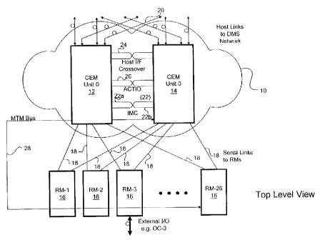
Figure 1 is a block diagram of the architecture of a communications system in
accordance with an aspect of the present invention;
Figure 2 is a block diagram of the architecture of a component of the
communications system of figure 1;
Figure 3 is a block diagram of the generic architecture of a further component
of the
communications system of figure 1;
Figure 4 is a block diagram of a signal processing resource module for use
with the
communications system of figure 1; and
Figure 5 is a block diagram of an interface resource module for use with the
communications system of figure 1.
DETAILED DESCRIPTION
Figure 1 illustrates the architecture of a modular communications system. A
common equipment module ("CEM") complex 10 comprises two CEMs 12, 14 (control
modules). The two CEMs are interconnected to each other. Each control module
12, -
-3 b-
CA 02266673 1999-03-17
WO 98/13961 PCT/CA97/00696
14 is connected to a plurality of resource modules 16 ("RMs") by way of
resource
module links 18. The resource module links 18 are also referred to as S-Links.
In this embodiment, upto twenty-six RMs may be connected to CEM complex 10
by S-links 18. Of course, a larger number of resource modules could be
connected to
an appropriately scaled system in accordance with the invention.
Each resource module link 18 is electrically isolated from every other
resource
link 18, effecting point-to-point connectivity between RMs 16 and CEMs 12,14.
This
allows for the isolation and easy detection of module failures. The ambiguity
in the
location of a fault is limited to at most 2 modules and the link between them.
The two CEMs 12, 14 operate in redundancy. One CEM (12 or 14) is active,
while the other remains inactive. Inactive CEM ( 14 or 12) is normally in
standby mode
ready to become active in the event of a failure on the presently active CEM
(12 or 14).
The exchange of activity is governed by software and hardware in each CEM 12,
14 and
is termed a "SWACT" (SWitch of ACTivity).
Similarly, RMs 16 can be provisioned with various redundancy schemes, as
required. One RM may serve as a redundant RM for one or more active RMs. In
the
event of a failure of an active RM payload data may be switched through a
redundant
RM. RM sparing is controlled by the CEMs. The CEM incorporate circuitry to
efficiently manage the transfer of payload data from a failed RM to a spare.
CEMs 12, 14 may further be interconnected to higher nodes in a host
communications system (for example DMS~' switch equipment) by way of host
interface
20 for the exchange of data with the host system. This allows the
communications
system to function as a peripheral subsystem. Of course, the communications
system
need not be connected to the host and may function as a stand-alone
communications
system.
-4-
CA 02266673 1999-03-17
WO 98/13961 PCT/CA97/00696
CEM complex 10 is the center for overall control and co-ordination of the
communications system. Complex 10 co-ordinates the setup and takedown of
connections
between RMs 16 or between RMs 16 and host interface 20, in response to
requests from
a host communications system (not shown). Complex 10 further allocates and de-
allocates system resources to calls and call events and coordinates resource
module
sparing operations and diagnostic operations.
RMs 16 supply payload processing capabilities to the communications system.
The number and type of RMs 16 required is application and provisioning
dependent.
RMs 16 can be broadly categorized by the type of resource they supply:
interface (e.g. 0C-3 Carrier);
pulse code modulation services (e.g. tone detection & generation, echo
cancelling);
messaging services (e.g. HDLC message format translation); or
computing services.
This modular design allows a communications system having specific
functionalities to be assembled from a small set of generalized components
(ie. RMs and
CEM). To provide sufficient and scalable control processing, distributed
computing
techniques are employed, with each RM 16 having its own processing capability
and
performing local low-level control functions under supervision of a central
control
component (ie. a CEM 12, 14). Thus, telecom functions are physically separated
into
control, interface, signalling and service modules. The alignment of the
physical and
logical partitioning allows the various functions to be efficiently mixed in
different
combinations with minimal new development. The architecture allows for
efficient
utilization of the switching function of CEMs 12,14 and RMs 16 by providing a
means
by which the amount of payload data exchanged with RMs 16 can be varied to
match the
requirements of a particular service circuit implementation, as more
particularly described
below.
-5-
CA 02266673 1999-03-17
WO 98/13961 PCT/CA97/00696
CEMs 12, 14 are interconnected to each other by way of intermodule
communications ("IMC") link 22; host data cross-over interface 24; and
activity
arbitration link 26.
IMC link 22 transports a set of signals used to exchange messaging data
between
CEMs 12 and 14. This facility allows software on an inactive CEM to track
operation
of software in the active CEM, thus keeping state data in the inactive CEM in
alignment
with that of the active CEM.
Host link 20 provides redundant communications signals between the
communications system equipment and higher nodes in a host system. These
signals are
used to carry payload data (e.g. PCM voice); messaging to other components of
the host
communications system which typically comprises DMS switch equipment; and
clocking
information. One CEM module provides one set of host links, while the other
CEM
module provides a redundant set.
Additionally Activity Input/output signals are exchanged between CEMs via link
26 to arbitrate for CEM Activity. As noted, only one CEM 12 or 14 is active at
any
time. The inactive CEM cannot disturb operation of the active CEM.
Resource module links 18 (or S-links) between the CEMs and resource modules
are serial links that,
transport payload voice and data bytes between the CEM complex 10 and the
RMs 16;
transport the system clock from the CEM complex 10 to RMs 16;
transport the CEM activity state from the CEM complex 10 to RMs 16;
transport low-level control (including RM reset control) from the CEM complex
to the RMs 16, and low level status from the RMs 16 to the CEM complex 10;
transport high level control and status between the CEM complex 10 and
the RMs 16 (messaging);
detect the presence or absence of an RM I6 by the CEM complex 10; and
-6-
CA 02266673 1999-03-17
WO 98/13961 PCT/CA97/00696
detect transport errors induced by electrical noise or other mechanisms.
All RMs 16 share a common interface definition (S-Link) to the CEMs 12, 14.
The maximum available payload bandwidth to an RM can be increased by
replicating the
S-Link interface as required. This enhances provisioning flexibility by
limiting the
number of distinct physical RM interface slot types.
Additionally, all resource and control modules are interconnected by way of a
common module test and maintenance bus ("MTM") 28, for transferring certain
diagnostic and control information between modules.
MTM bus 28 allows the active CEM 12 or 14 or external test equipment to
initiate
hardware tests of the communications system components. In addition, MTM bus
28 can
be used at the factory to store initial software loads in non-violative
storage on
communications system components. MTM bus 28 is also used during operation to
control visual indicators on each system component. MTM bus 28 is based on the
known
Joint Test Action Group (JTAG) 1149.5 specification.
A functional block diagram of CEM 12 or 14 is shown in Figure 2. Each CEM
12, 14 comprises a microprocessor 30 with associated data and program memory
32, and
a Processor Bus Access Chip 34 ("PBAC") application specific integrated
circuit
("ASIC"). PBAC 34 distributes the processor address and data signals to the
other
devices on the module so that the processor can control the other devices.
Clock 58 provides a clock signal for the CEM. The clock of the active CEM acts
as the system clock 58 for the communications system. A system clock signal
flows from
the CEM complex 10 to the RMs 16 via S-links 18. The clock of the inactive CEM
is
synchronized to the clock of the active CEM. In addition, system clock 58 can
be
synchronized to the Host Interface 20 or a particular RM 16.
CA 02266673 1999-03-17
WO 98/13961 PCT/CA97/00696
Intelligent Test Master ("ITM") device 59 operates under supervision of the
microprocessor 30 to control scan test and Built In Self Test (BIST)
operations for CEMs
12 and 14 as well as tests of other modules by interfacing with the MTM bus
28.
Each CEM 12, 14 contains a switching matrix which allows payload data
timeslots
to be connected between the host interface and the RMs 16, or between RMs 16.
Additionally, each CEM 12, 14 provides a facility to relay control and status
messages
between the host interface 20 and RMs 16 or between RMs 16.
Each matrix is comprised of a bandwidth allocator 36a, 36b ("BWA ") and a time
division multiplex switch 38.
Time switch 38 provides a payload switching function with 1 timeslot
resolution.
Each timeslot comprises 8 bits of payload data, a spare bit and a parity bit
(typically odd parity). Each timeslot may transport payload data (i.e. voice);
overhead
data; signalling information; or messaging information.
BWA 36a, 36b comprises a bandwidth selector 36a and bandwidth distributor 36b.
The bandwidth selector 36a and the bandwidth distributor 36b each comprise
their own
matrix. Bandwidth selector and bandwidth distributor matrices have a payload
switching
function with 32 timeslot resolution.
Also included in the switching matrix is a padding block 40 ("PADS") which
allows simple (unary) operations to be performed on the data stream output by
timeswitch
38 by means of a set of Look-Up Tables. Each timeslot in the stream can be
manipulated
separately.
S-Links 18 are connected to the RMs 16 by a set of six S-Link Interface Master
(SLIF-M) 54a, 54b devices. The SLIF-M devices 54a, 54b function as an
input/output
point for transferring payload and control data between the CEM complex 10 and
RMs
16. Physically, each S-link 18 is interconnected to a CEM 12, 14 at a single
point. For
_g_
CA 02266673 1999-03-17
WO 98/13961 PCT/CA97/00696
clarity, figure 2 illustrates the separate connection points for transferring
data from S-
links 18 to CEM via SLIF-M 54a, and transferring data from the S-links to the
CEM via
SLIF-M 54b. The 5LIF-M device 54a, 54b is interconnected to the BWA selector
36a
and BWA distributor 36b.
The selection portion 36a of the BWA collects input payload streams from the
host
via the host interface 20 and RMs 16 and presents a selected portion of the
total payload
capacity to timeswitch 38. The distribution portion 36b of the BWA collects
the switched
payload from the timeswitch 38 and distributes it to the host interface 20 and
RMs 16.
The host interface 20 connects the CEM complex 10 to a host communications
system (not shown). Host interface 20 is comprised of a quad link controller
("QLC")
44a, 44b and channel supervisory message ("CSM") device 46a, 46b. QLC device
44a,
44b functions as an input/output point for transferring payload and messaging
data
between the CEM complex 10 and other components of the host equipment.
The communications system also uses processor to processor messaging to
exchange control and status information between RMs 16, CEMs 12, 14 and/or a
host.
Messaging functions are supplied by two devices. The Link Protocol Message
Interface
Chip ("LPMIC") 48 translates messages between the payload stream and the
processor
memory. The system mapper/tracer ("SMT") 50 is an optional device which
permits
message routing without processor intervention and provides a mechanism by
which the
processor can trace message flow within the system.
The LPMIC 48 serves to transfer messaging data between the microprocessor 30
and the payload data stream, which is subsequently routed by the BWA 36a, 36b
and
other devices. It terminates up to thirty-two messaging ports, using known
DMS'
messaging protocols. Each port communicates via an exchange of data with a
similar
port at the other terminating end.
As noted above, RMs 16 supply payload processing capabilities for the
communications system and RMs 16 can be broadly categorized by the type of
resource
-9-
CA 02266673 1999-03-17
WO 98/13961 PCT/CA97/00696
they supply: interface; PCM services; messaging services; or computing
services. The
number and type of RMs 16 required is application and provisioning dependent.
Figure 3 illustrates the generic architecture of an RM. In order to allow for
the
flexible configuration of the communications system; RM sparing; and a uniform
interface between RMs and the CEM complex 10, all RMs should conform to this
architecture .
Each RM 16 comprises a serial link interface slave (SLIF-S) device 110. SLIF-S
device 110 functions as an input/output point for transferring payload and
control data
between the CEM complex 10 and the RMs 16. SLIF-S device 110 interconnects to
S-
links 18, and ultimately connects to SLIF-M devices 54a, 54b of CEMs 12 and
14.
SLIF-S device 110 is additionally interconnected to module specific circuitry
112 which
implements processing functions of RM 16.
Additionally, each RM 16 also comprises its own microprocessor and memory 114
to interact with the SLIF-S device 110 and the module specific circuitry.
Moreover, the
RM processor 114 is able to communicate with both active and inactive CEMs.
Normally, however, the software on the microprocessor 114 responds solely to
message
requesting operations in the payload data of originating with the active CEM.
Each RM 16 also comprises an ITM device 116 connected to the MTM bus 28
and an 1149.1 test bus on RM 16. Under commands on the MTM bus 28 (provided by
the active CEM 12, 14) diagnostic and self test can be invoked on components
of RM 16.
Figure 4, illustrates the architecture of a digital signal processing ("DSP")
RM
130, for use with the communications system. Consistent with generic RM
architecture,
the DSP RM 130 comprises SLIF-S device 132, interconnected to microprocessor
and
memory 134.
- 10-
CA 02266673 1999-03-17
WO 98/13961 PCT/CA97/00696
The DSP RM 130 provides digital signal processing capability to the
communications system, capable of operating on channels of payload DSOs data.
Functionality is, of course, dependent on software contained on DSP RM 130.
Typically,
the DSP RM is employed for,
tone generation, such as DTMF, MF, Dialtone, etc;
tone detection, such as DTMF, MF, Special Tones;
AB Bit Generation; or
AB Bit filtering and scanning.
Possible future DSP functions include voice recognition; voice playback; and
data
compression/decompression.
For DSP RM 130, the resource module specific circuitry 136 consists of a
number
of DSP Islands 138 operating on the payload data provided via bus 140 and 142.
Each
DSP island 138 consists of a DSP processor 144 with associated Random Access
Memory
(RAM) 148 and an interface device (DIA) 146. DIA devices 146 select and buffer
payload data incoming via bus 138 and present it to DSP processor 144 for
access by the
DSP software. Payload data generated by the DSP processor 144 is buffered by
DIA 146
and output on the outgoing payload bus 142. The capabilities of DSP RM 130 can
be
scaled by varying the quantity of DSP islands 138, and the type of DSP
processor 144.
The DSP RM 130 further comprises microprocessor 134 which messages with,
and downloads software to, the DSP processors 144 via the DIA devices 146 and
processor bus 150. Typically, these messages instruct the DSP processors 144
to enable
or disable a service or query the results of a service such as tone detection,
and would
be issued by the microprocessor in response to a message received from CEMs
12, 14.
The communications system implements two types of DSP RMs: a geaeral
purpose DSP and a high capacity VSP (Voice Services Processor). The general
purpose
DSP and VSP differ only in the quantity and type of the DSP islands 138. The
VSP
provides computationally intensive digital signal processing capability for
use with the
-11-
CA 02266673 1999-03-17
WO 98/13961 PCT/CA97/00696
communications system and operates on payload DSO channels of data.
Functionality is
dependent on software contained on the VSP RM. A typical application would be
to
supply Echo Cancelling capability.
Figure 5, further illustrates the architecture of an OC-3 interface RM. This
RM supplies a SONET intra-office interface at the known OC-3 rate ( 155.52 Meg
Bits
per second). Typical applications would be to supply a trunk interface or
interface to
an Integrated Digital Loop Carrier (IDLC).
The OC-3 RM performs:
Electrical/Optical conversion;
SONET clock recovery and framing;
SONET line and section overhead generation and termination;
mapping of DS3 and constituent DSls into SONET;
mapping of DSls into SONET VT1.5 Synchronous format;
DS 1 framing (up to 84 DS 1 s};
mapping of DSOs into SONET VT1.5 Byte Synchronous format;
mapping of DSOs into DS 1 format;
slip buffering of DSOs to align with communications system clock;
signalling bit (ABCD bit) Extraction and Insertion;
performance monitoring at all carrier levels;
supplying a reference signal to the CEM complex to synchronize the Spectrum
system clock to the incoming OC-3 carrier; and
local diagnostics and loopback control.
0C-3 RM 160 is capable of terminating the full voice payload (2016 DSOs) in
various formats including, Asynchronously Mapped VTl.Ss; Bytesynchronously
Mapped VTl.Ss and Asynchronously mapped DS3s.
To achieve the required payload bandwidth, OC-3 RM 160 comprises three SLIF-
S devices 162x, 162b, 162c with associated S-Link clusters, one for each STS-1
- 12-
CA 02266673 1999-03-17
WO 98/13961 PCT/CA97/00696
component of the OC-3 signal.
These three SLIF-S devices are interconnected with one of the three Path
Termination blocks 178a, 178b, 178c via busses 180a, 180b, 180c, 182x, 182b,
182c.
Each block assembles twenty-eight VTl.Ss or one DS3 from the payload
datastream,
using the overhead payload timeslots to generate the AB signalling bits if
required.
The Path Termination blocks 178a, 178b, 178c are further interconnected to
Section and Line Overhead Termination block 182 where SONET Section and Line
overhead data are added as per SONET specifications. Data for the outgoing
Section and
Line Data Communications Channels are supplied by microprocessor 174 which
controls
overall operation of the OC-3 RM. Optical Interface block 164 serializes and
converts
data to optical form.
Clocks to drive the SONET mapping circuitry are generated by Phase Locked
Loop ("PLL") 184, which is locked to the frame rate of the active CEM (12 or
14).
In operation, the communications system switches payload and messaging data
between a CEMs 12, 14; a host communications system (not shown); and a
plurality of
RMs 16.
Data is received by the system via the host communications
system and/or via those RMs 16 having external links. These external links may
be
telephone subscriber lines or trunks to other switches. The data received by
the system
is typically channelized in multiple DSO (64kbps) data channels.
Referencing Figure 5, for data received by an OC-3 RM, an incoming optical OC-
3 signal is received by optical interface 164 via optical link 166 and
converted to
electrical form. A clock waveform is extracted by optical interface 164. The
frame
indicator is located, and the data converted to byte wide parallel form.
-13-
CA 02266673 1999-03-17
WO 98/13961 PCT/CA97/00696
The parallel data is passed to section/line termination block 182 via bus 168.
In
section and line overhead termination block 182, the overhead bytes are
processed
according to known SONET specifications. Data from Section and Line Data
Communications channels is extracted, and presented to the OC-3 RM
microprocessor
174 via bus 172. The payload data from each STS-1 component of the datastream
is
forwarded to one of three identical Path Termination blocks 178a, 178b, 178c.
Each
block operates on one STS-1 component signal in either DS3 or VT1.5 format.
The path
termination blocks 178a, 178b, 178c complete the process of extracting DSOs
from
VTI.Ss or DS3s and pass the resulting parallel stream of timeslots (~ to the
SLIF-S
devices 162a, 162b, 162c. Signalling data (AB bits) are extracted and passed
as
overhead payload timeslots to SLIF-S devices 162a, 162b, 162c via bus 180a,
180b,
180c. The individual DS1 or VT1.5 components are slip buffered to align them
with the
communications system frame rate.
The payload data provided to SLIF-S devices 162a, 162b, and 162c is then
provided to the CEMs over S-links 18. Additionally, software executing on the
OC-3
RM microprocessor 174 monitors the carrier signals for alarm conditions, and
notifies
the CEM processors 30 of alarm events by messaging through the SLIF-S
interface 162a,
162b, 162c via bus 175 and bus 177.
Data received by the system from the host is provided to the CEM complex 10
(Figure 2) via host link 20 to the QLC 44a. QLC 44a receives four serial
streams of 512
twelve bit timeslots per frame each from four Optical/Electrical conversion
modules 60.
Within this data, the QLC 44a locates a frame identifier and monitors the
cyclic
redundancy check characters for errors. QLC 44a performs serial to parallel
conversion
on the four data streams and converts the twelve bit data streams to ten bit
streams
(12B10B decoding). In order to align each stream to the CEM system clock 58,
QLC
44a performs a slip buffer operation of each data stream. The slip buffer
deletes or
duplicates entire intact frames of data if required to align the payload
stream to the CEM
clock 58. On reading the data from the slip buffer, QLC 44a interleaves the
four streams
to create a unified stream of 2048 timeslots per frame (ten bits per timeslot)
to be
forwarded to CSM device 46a via bus 52. A second, identical, stream is created
- 14-
CA 02266673 1999-03-17
WO 98/13961 PCT/CA97/00696
independently to be forwarded to the CSM device of the mate CEM module (not
shown
in Figure 2) via bus 62.
CSM device 46a accepts the stream of ten bit timeslots, 2048 timeslots per
frame
from the QLC 44a and accepts a similar stream from the QLC device of the mate
CEM
(not shown) via bus 64. Independently, on both streams, the CSM 46a decodes
the
channel supervisory message information (messaging data) from each timeslot
and makes
the results available to microprocessor 30 and creates an output stream of
payload data
which is provided to the selector portion of BWA 36a via bus 58. The data from
the
QLC device 44a is selected from the active CEM or the mate CEM on a per-
timeslot
basis. Data is selected by verifying information present in the received CSM
information. If one stream exhibits incorrect CSM information, the other
stream is used.
The automatic selection process can also be over-ridden by microprocessor 30
on a per-
timeslot basis.
Using the selected stream, CSM 46a creates a further output stream which is
provided to LPMIC 48 via bus 66. This output stream is generated by merging
data on
messaging bus 68 with data from QLC device 44a (via bus 52) or the QLC device
of the
mate (via bus 64). Selection is on a per-timeslot basis, and is under control
of
microprocessor 30. The output data stream contains interleaved messaging data
from the
host interface on the mate (inactive) CEM via bus 64 or bus 52 from host
interface 20
via QLC 44a and from RMs 16 and IMC 22a via bus 68 and the inactive CEM via
IMC
22.
LPMIC device 48, accepts this data stream of 4096 timeslots per frame from the
CSM device 46a via bus 66. This data stream contains messaging information
from up
to 32 originator ports in other modules. LPMIC 48 then assigns the timeslots
to
messaging ports, under control of a connection memory 70 initialized by
microprocessor
30 and terminates the messaging protocol present on each port, and buffers the
received
message. The messaging bandwidth of an individual port can be set by assigning
the
desired number of timeslots to that port. A given port may be assigned up to
2048
timeslots by connection memory -- connected to LPMIC 48. Thereafter, LPMIC 48
-15-
CA 02266673 1999-03-17
WO 9$/13961 PCT/CA97/00696
transfers the received message to the microprocessor's memory 32 via the
transaction ST
bus 72, using Direct Memory Access ("DMA ") techniques.
Upon notification by microprocessor 30, LPMIC 48 also retrieves message data
from the microprocessor's memory 32 via ST bus 72, using DMA techniques, and
buffers the message data locally. Based on values in the microprocessor's
memory,
LPMIC 48 directs the message data to one of the 32 messaging ports, but first
encodes
the message data with the protocol for that port. It outputs the encoded
message to the
BWA 36b and CSM device 46b via 4096 timeslot bus 74. The assignment of message
ports to timeslots on bus 74 is under control of the connection memory 70
initialized by
microprocessor 30.
SMT 76 is an optional component which adds message mapping and tracing
functionality to the CEM. If SMT device 76 is present, LPMIC 48 can
alternatively re-
route a received message to the transmit side of another messaging port
without
intervention by microprocessor 30, thus providing message relay services.
This is accomplished by LPMIC 48 device presenting certain data values in the
message (representing a logical endpoint address) to SMT device 76 via the ST
bus 72.
SMT device 76 then compares the logical address against values stored in a
routing table
in the device to determine which physical messaging port the message should be
routed
to. The selected physical port number is then transferred to LPMIC 48 which
performs
the actual message transfer. In the case where the physical address is the
module itself,
LPMIC 48 transfers the message to the microprocessor's memory 32 as above.
These
operations can occur on the ST bus 72 independently of the microprocessor's
memory
bus. The values in the SMT routing table are initialized by microprocessor 30.
SMT device 76 can also trace message transactions, by observing and recording
in a memory buffer addressing information contained in the message data as it
is
transferred on ST bus 72.
-16-
CA 02266673 1999-03-17
WO 98/13961 PCT/CA97/00696
If SMT device 76 is not present, all messages are transferred to
microprocessor
memory 32, and the above operations may be performed by software by
microprocessor
30.
Data provided to the CEM complex 10 from RMs 16 is provided via S-links 18
to SLIF-M device 54a, 54b. Each SLIF-M 54a, 54b device receives 16 serial
streams
of 256 timeslots per frame each with associated clocks from the RMs 16 via S-
links 18,
organized as five clusters. Typically one cluster originates with each RM (3
in the case
of an OC3 RM).
SLIF-S device (Figure 3) of each RM providing data to the CEM complex accepts
a stream of ten bit parallel data from RM specific circuitry 112. It then
creates two
identical copies of the payload data. On both copies of the payload data,
messaging data
is inserted from RM microprocessor 114. The messaging data inserted on both
streams
need not be identical. SLIF-S device 110 further calculates a cyclic
redundancy check
for both streams, and converts them to serial format for transmission to both
CEMs (one
serial data stream to active CEM, and one to inactive CEM) via S-links 18.
SLIF-M device 54a, 54b (Figure 2) of the CEMs receives this data and locates
the
frame identifier and verifies the cyclic redundancy check characters for error
monitoring
purposes; performs a Serial to Parallel conversion on each of the data
streams; interleaves
the resulting parallel data into a single parallel stream of 4096 timeslots
per frame; and
outputs this stream to the BWA selection device 36a via bus 56.
Under control of microprocessor 30, the SLIF-M 54a device is capable of
looping
received data around to the transmit portion of the SLIF-M device 54b for
diagnostic
purposes. Physically, the receive and transmit portions of the SLIF-M device
54a, 54b
are formed in a single ASIC, which facilitates this data looping.
BWA 36a, 36b is implemented in two components (Selection 36a and Distribution
36b) . Each component provides a coarse (thirty-two timeslot resolution) data
switching
facility, operating on payload data to and from the RMs 16 and the host
interface 20.
- 17-
CA 02266673 1999-03-17
WO 98/13961 PCT/CA97/00696
It further merges messaging data to and from IMC link 22 and RMs 16 with the
payload
data.
On the selection side, the BWA 36a accepts data streams from the SLIF-M device
54a containing payload and messaging timeslots via bus 56. It further accepts
a data
stream from the CSM device 46a via bus 58 containing payload timeslots and
generates
a new data stream containing payload timeslots which is forwarded to the
timeswitch
device 38 via bus 80. This stream contains a selected subset of the payload
timeslots
from the SLIF-M 54a and host interfaces 20. Additionally, the BWA 36a accepts
a
further data stream containing IMC messaging timeslots from the Distribution
side of the
BWA on the mate CEM via bus 82. BWA 36a then generates new data stream
containing message timeslots from the IMC stream and from the RMs (via SLIF-M
54a
and bus 56), which is forwarded to the CSM device 46a via bus 68.
Data from the BWA selection device 36a is provided to timeswitch 38 via bus
80. Within timeswitch 38 the data is written into one of two memory buffers in
consecutive memory addresses within the timeswitch. Each buffer can store a
full frame
of data. Simultaneously, data are read out of the second memory buffer via bus
82, with
buffer addresses supplied by a third memory 84 (Connection Memory via bus 87).
Within each frame, the buffers exchange functions. The output data is
forwarded to the
padding function 40. Addressing of connection memory 84 is sequential and
repeats
every frame. Connection Memory 84 is also accessible by microprocessor 30.
By writing values (buffer addresses) in the connection memory 84,
microprocessor
30 causes the timeslot ordering of the output data stream to be rearranged
with respect
to the ordering of the input stream, thus accomplishing the switching
function. The
timeswitch is used primarily by call processing software.
The output of the timeswitch is provided to PADS 40 which performs unitary
operations on the datastream. Operation is by table look-up. A new data stream
is formed
by concatenating the payload stream provided via bus 82 with a stream of data
from
connection memory 84 via bus 86. Connection memory 84 has' one location for
each
- I8-
CA 02266673 1999-03-17
WO 98/13961 PCT/CA97/00696
timeslot, and is read out sequentially each frame. As noted above, connection
memory
84 is accessible by microprocessor 30, so that it may vary the memory
contents.
The new data stream passed to PADS 40 via bus 82 may be regarded as having
two components: the value from timeswitch 80 (index within a table), and the
value from
the connection memory 84 (table selection). This data stream is used to
address a set of
tables stored in Read Only Memory (ROM).
The output data from the ROM is used as the output of PADS 40 and is used as
the new (modified) payload data stream. The data values stored in the ROM
represent
precalculated outputs for the following operations:
- No change to payload data (Unity Gain)
- Various levels of Gain and Attenuation, when the payload data is
formatted as Pulse Code Modulation (PCM) voice samples
- Conversion between the A-Law and u-Law PCM encoding standards.
This data is provided via bus 88 to the distribution side of BWA 36b. The
distribution side of BWA 36b accepts the data stream from the PADs block 40
containing
payload timeslots via bus 88, it further accepts a data stream via bus 74
containing
messaging timeslots from the LPMIC device 48; it generates new data streams
containing
payload and messaging timeslots which are forwarded to the SLIF-M devices 54b
via bus
90. The BWA 36b further generates a new data stream containing payload
timeslots
which is forwarded to the CSM device via bus 92 and a further new data stream
containing messaging timeslots (IMC) which is forwarded to the selection side
of the
BWA on the mate CEM via bus 94.
Within the BWA 36a, 36b, timeslots from the inputs are written into one of two
memory buffers in consecutive memory locations. Each buffer can store 1/32 of
the
number of input timeslots per frame. Simultaneously, data is read out from the
second
buffer. The two buffers exchange functions thirty-two times per frame. Memory
addresses for the read operation are supplied by sequentially reading a third
memory 84
- 19-
CA 02266673 1999-03-17
WO 98/13961 PCT/CA97/00696
containing connection instructions. The values in the connection memory 84 can
be
accessed by microprocessor 30.
By writing values in connection memory 84, microprocessor 30 causes timeslot
ordering of the output data stream from BWA 36b to be rearranged with respect
to that
of the input stream, thereby switching the data contained in the timeslots.
Since the
connection process is repeated thirty-two times per frame, each parameter in
the
connection memory is used thirty-two times per frame. Thus the thirty-two
timeslots
controlled by a given connection parameter are treated as a unit in that all
thirty-two
affected timeslots are switched identically. Such a collection of timeslots is
referred to
as a Bandwidth Allocator Group.
As is apparent, these Bandwidth Allocator Groups are interleaved so that one
timeslot from each Group is processed by the buffer per exchange time.
Selector portion 36a of the BWA is similarly capable of switching Bandwidth
Allocator Groups
BWA 36a, 36b is also capable of broadcasting one input group to more than one
output group. BWA 36a, 36b is however not capable of rearranging timeslots
within a
BWA Group.
This switching function of BWA 36a, 36b is used primarily for
(1) provisioning (Bandwidth allocation for RMs); and
(2) fault recovery software.
Por provisioning operations, the amount of bandwidth allocated to a given RM
slot
can be adjusted according to the RM's function. This grooming of the bandwidth
allows
the time division multipped switch 38 have less capacity (handle less
timeslots) than the
aggregate payload bandwidth present on buses 56, 50, 42 and 42.
-20-
CA 02266673 1999-03-17
WO 98/13961 PCT/CA97/00696
For maintenance or fault recovery operations on RMs 16, the payload bandwidth
to and from a given RM can be switched to a spare RM without disturbing the
connections in the timeswitch function. Since timeslots are switched in groups
of 32 at
most 1/32 of the number of connection parameters that would be required need
to be
changed, this is faster than performing the equivalent operation in the
timeswitch 38. In
addition, the operation can be performed without disturbing the connection
parameters
of the time division multiplexed 38, helping to isolate the maintenance and
provisioning
software functions from the call processing software functions.
Because the BWA 36a, 36b is a full matrix, as opposed to a data multiplexer,
the
slot location of the spare RM need not have any special relationship to the
working RM.
This flexibility allows for 1 + 1, N + 1, and N + M RM sparing configurations.
Selection
between redundant and active RMs is controlled by microprocessor 30.
As an example of 1 + 1 RM sparing, consider a resource "X" supplied by RM 16
"A", with an additional RM 16 "B" serving as the spare RM. RM 16 "B" is
configured
in an identical manner to RM 16 "A", such that working and spare resources "X"
from
RM 16 "A" and RM 16 "B" respectively are transported in the same timeslots
(and
therefore corresponding BWA Groups) on S-Links 18.
A sufficient number of timeslots in timeswitch 38 are assigned to make the
resources "X" available as call processing functions. The number of timeslots
will be
a multiple of the BWA Group size (i.e. 32). Microprocessor 30 has set the
connection
parameters of BWA 36a such that the BWA groups from RM 16 "A" are presented to
the timeswitch 38 via datastream 80. Additionally, microprocessor 30 has set
the
connection parameters of BWA 36b such that the timeslots from the timeswitch
38
corresponding to these resources are presented identically via S-Links 18 to
both RM 16
"A" and RM 16 "B" . Thus when a call processing connection is made in
timeswitch 38
from one of the resources "X", the payload data is selected by BWA 36a from RM
16
"A"; correspondingly when a call processing connection in timeswitch 38 is
made to one
of the resources "X", the payload data is sent identically by BWA 36b to both
RM 16
"A" and RM 16 "B". The resource "X" is thus supplied by RM 16 "A".
-21 -
CA 02266673 1999-03-17
WO 98/13961 PCT/CA97/00696
When maintenance software executing on microprocessor 30 decides to perform
the RM sparing operation, as may happen in the event of a failure of RM 16
"A", it
manipulates the connection parameters in BWA 36a such that the BWA groups from
RM
16 "B" are presented to timeswitch 38, replacing those previously connected
from RM
16 "A". The connection parameters of BWA 36b are not altered. Connections in
timeswitch 38 are not altered. The resources "X" said above are now being
supplied by
RM 16 "B".
As an example of N+ 1 RM sparing, consider a resource "X" supplied by RM 16
"A", and another resource "Y" supplied by a different RM 16 "B", with yet
another RM
16 "C" serving as the spare RM. RM 16 "C" can be configured by software, if
required,
to be equivalent to either RM 16 "A" or RM 16 "B". Initially, microprocessor
30 has
set the connection parameters in BWA 36a such that the timeslots corresponding
to
resource "X" are presented to timeswitch 38 from RM 16 "A", and the timeslots
corresponding to resource "Y" are presented to timeswitch 38 from RM "B". The
timeslots from RM 16 "C" are not used, and by virtue of not being connected in
BWA
36a do not consume capacity of timeswitch 38. Similarly, microprocessor 30 has
configured BWA 36b such that the timeslots from timeswitch 38 corresponding to
resource "X" are sent to RM 16 "A", and those for resource "Y" are sent to RM
16 "B".
Microprocessor 30 also sets the connection parameters of BWA 36b such that RM
16 "C"
receives identical payload data to that of RM 16 "A" or alternatively RM 16
"B". For
this example, assume RM 16 "A". Said resources "X" are being supplied by RM 16
"A", and said resources "Y" are being supplied by RM 16 "B".
When maintenance software executing on microprocessor 30 decides to spare RM
16 "B" with RM 16 "C" , it first sends a message to RM 16 "C" (via LPMIC 48),
instructing the microprocessor 114 present on RM 16 "C" to configure RM 16 "C"
to be
identical to RM 16 "B" . Microprocessor 30 then alters the connection
parameters of
BWA 36b such that the timeslots from the timeswitch 38 corresponding to the
resource
"Y" are presented identically via S-Links 78 to both RM 16 "B" and RM 16 "C".
Payload data destined for resource "Y" is now sent identically to both RM 16
"B" and
RM 16 "C". Finally, microprocessor 30 manipulates the connection parameters in
BWA
-22-
CA 02266673 1999-03-17
WO 98/13961 PCTlCA97/00696
36a such that the BWA groups from RM 16 "C" are presented to timeswitch 38,
replacing those previously connected from RM 16 "B". Connections in timeswitch
38
are not altered. The resources "Y" said above are now being supplied by RM 16
"C".
The resources "X" said above are still supplied by RM 16 "A".
Data from the distributor side of the BWA 36b is provided to transmit portion
of
CSM 46a, 46b. The CSM 46b accepts a stream of 10 bit timeslots, 2048 timeslots
per
frame from the distribution side of BWA 36b via bus 92. The CSM 116b adds a
data
stream (Channel Supervisory Message) to one of the bits of each timeslot,
according to
the requirements of DMS switching equipment. Each of the 2048 timeslots may
have a
unique CSM stream. Values for the CSM stream are supplied by microprocessor
30.
This stream is merged with data from the Tx message bus 74 by selecting
between the
payload stream and message bus 74 on a per timeslot basis. CSM 46b then
outputs the
resulting stream to the mate CEM (not shown) via bus 96, and also to an
elastic store
mechanism. CSM 46b similarly accepts a stream via bus 98 from the mate CEM
(not
shown) and applies it to a second elastic store mechanism. The purpose of the
elastic
store mechanisms is to allow for small misalignments between the frames of the
two
CEMs 12 and 14. CSM 46b further reads two data streams from the elastic stores
and
creates an output stream by selecting data from one elastic store or the
other. Normally,
data created by the active CEM is used, but this can be over-ridden on a
timeslot basis
to allow the CEMs to share the output data stream. The resulting data stream
is provided
to the QLC device 44b via bus 100.
QLC device 44b receives a stream of 2048 interleaved ten bit payload data per
frame from the CSM device 44b via bus 100, and converts the stream of ten bit
payload
data into a stream of twelve bit data ( lOB 12B encoding) suitable for optical
transmission.
It further adds Link overhead bits (Frame identifier and cyclic redundancy
check
characters for error detection). Moreover, it converts the payload stream into
four
serialized streams of 512 timeslots per frame each and outputs the serial
streams to four
Electrical/Optical conversion modules 162 for transmission from the CEM module
to the
host via host interface 20. The rate of payload transmission is determined by
whichever
CEM is in the active state.
-23-
CA 02266673 1999-03-17
WO 98/13961 PCT/CA97/00696
The distributor portion 36b of BWA 36a, 36b further provides the (Tx) portion
of the SLIF-M device 54b a stream of 4096 interleaved ten bit payload data per
frame
in parallel format via bus 90. The SLIF-M device 54b adds link overhead bits
(Frame
identifier and Cyclic Redundancy Check characters for error detection); adds
information
bits indicating the activity state of the CEM; converts the data to sixteen
serialized
streams of 256 timeslots per frame each, organized as five clusters each of
three streams
and one cluster of one stream; and outputs the sixteen data streams with
associated bit
clocks to the RMs via S-links 78.
At RMs 16 (Figure 3), the SLIF-S devices 110 receive a datastream containing
switched payload and messaging data from each CEM 12, 14 via S-links 18. Up to
three
S-links form a cluster provided by each CEM to an RM 16. The SLIF-S devices
110
locate and extract frame indicators inserted by the SLIF-M devices 54b from
each cluster.
The SLIF-S device 110 also monitors the integrity of the data by verifying the
CRC
inserted by the SLIF-M device 54b. It also extracts activity information from
each
stream to determine which stream originated with the active and inactive CEM.
Data is
always selected from the active CEM. The CEM activity states are known by
special
indicator bits in serial data carried by S-links 18. The indicator bits from a
given S-link
18 are used in the selection algorithm only if the CRC for that stream
indicates that the
data is not corrupt. Thereafter, the serial streams are converted to ten-bit
parallel
streams or interleaved data. SLIF-S 1I0 then creates a single parallel data
stream by
selecting the active data inactive stream which is provided to resource module
specific
circuity 112 via bus 120. The SLIF-S device 110 also extracts messaging data
from both
streams and forwards the messaging data to RM microprocessor 114 via bus 118.
Resource module specific circuitry 112 then processes the data as required by
the
RM.
A person skilled in the art will appreciate that numerous modifications to the
preferred embodiment are possible. For example, the system may be scaled to
allow
different numbers of RMs or CEMs accommodating larger payloads. Similarly, the
rate,
number, payload capacity or format of S-links 18 or Host link 20 could be
varied. For
-24-
CA 02266673 1999-03-17
WO 98/13961 PCT/CA97/00696
example, optical links could be used for S-links. Similarly, the size of
timeswitch 38
could be modified, or the granularity or size of the switches in the BWA could
be
altered. Similarly, bus sizes and messaging protocols within RMs 10 and CEM
12, 14
could be varied.
A further possible variation is to provide an additional payload path between
BWA
36a and 36b, acting as a shunt across a portion of timeswitch 38. This path
would in
effect operate as a portion of the timeswitch 38 with a fixed set of
connections, useful for
applications not requiring payload switching at granularities other than that
of the BWA
36a and 36b. Since the frame alignments at the input 80 and output 82 of
timeswitch 38
are approximately equal, this path could be economically implemented with a
few latches.
Payload switched through this path would not experience the frame buffering
delay of
timeswitch 38. In this scenario, the functions and purposes of the BWA 36a and
36b
remain unchanged.
Those skilled in the art will further recognize that various modifications,
and
changes to the above described preferred embodiments are possible without
departing
from the spirit or scope of the invention as defined by the claims.
-25-