Note: Descriptions are shown in the official language in which they were submitted.
CA 02267018 1999-03-26
-1-
OPTICAL WAVELENGTH CONVERTER
WITH ACTIVE WAVEGUIDE
Background of the Invention
Field of the Invention
The present invention relaters to an optical wavelength
converter for converting an input optical pulse signal having a first
wavelength into an output optical pulse signal having a second
wavelength which is different from said first wavelength.
Description of the Related Art
Such an optical wavelength converter can be preferably used
as a resource in the wavelength division multiplex (WDM) optical
communication system. In accordance with a recent abrupt progress in
the digital communication system, the; development of the WDM optical
communication system has been strongly required. This WDM optical
communication system requires an optical wavelength converter in
order to utilize channels in an efficient manner by channel switching.
Such an optical wavelength converter has been known. For instance, a
XGM type optical wavelength converter utilizing a cross gain
modulation has been proposed. In tine XGM type optical wavelength
converter, an intensity-modulated input optical signal having a
wavelength ~,~ and an optical signal having a wavelength ~2 and a
constant amplitude are supplied to a semiconductor optical amplifier,
and a polarity-inverted output optical signal having a wavelength ~,2 is
produced by utilizing a difference in lain for an optical power
impinging upon the semiconductor optical amplifier.
There has been further proposed a XPM optical type optical
wavelength converter. A conventional type optical wavelength
converter utilizes the principle of Mach-Zehnder type interferometer.
98144 (10-273,435)
CA 02267018 1999-03-26
-2-
An input side waveguide upon which an input optical signal having a
wavelength ~,1 is divided into two waveguides, a semiconductor optical
amplifier is arranged in one of the waveguides, and these two
waveguides are set to be in-phase for light having a wavelength ~,2 to be
modulated. When an input optical signal having a wavelength ~,1 and
an optical signal having a wavelength ~,2 and a constant amplitude
propagate, there is produced a phase difference of a half wavelength
between the two waveguides due to the function of the input optical
signal. By utilizing this phase difference, an inverted optical output
having the wavelength ~,2 is generated..
In the known XGM type optical wavelength converter, since
the output optical signal having a wavelength ~,2 produced in response to
the input optical signal having a wavelength ~,I has a rather small gain.
Therefore, a zero level of the output optical signal deviates from a real
zero. This results in that the extinction ratio of this optical wavelength
converter is small.
In the above mentioned XPIVI type optical wavelength
converter, although it is possible to obtain a sufficiently large extinction
ratio, since it reveals a periodical response, an extremely severer
tolerance is required for a device length. Therefore, a through-put of
the known XPM type optical wavelength converter.
Furthermore, the above mentioned known optical wavelength
converter is relatively large in size. That is to say, the typical size of
the known optical wavelength converter is not smaller than several to
ten millimeters, and thus it is practically difficult to integrate it as a
single chip.
Summary of th.e Invention
The present invention has for its object to provide a novel and
98144(10-273,435)
CA 02267018 1999-03-26
-3-
useful optical wavelength converter which can avoid or at least mitigate
the above explained problems of the known optical wavelength
converters and can have a large extincaion ratio, can operate even in a
digital fashion, and can be manufactured easily.
It is another object of the invention to provide an optical
wavelength converter which can be small in size and can be integrated
as a single chip.
According to the invention, an optical wavelength converter
for converting an input optical pulse signal having a first wavelength
into an output optical pulse signal having a second wavelength which is
different from said first wavelength comprises:
a first waveguide constructed by an active waveguide and receiving
the input optical signal having the fir:~t wavelength, a propagation
constant of said first waveguide being; changed in accordance with the
input optical signal; and
a second waveguide arranged in parallel with said first waveguide
to partially overlap with said first waveguide such that the first and
second waveguides are optically coupled with each other to such an
extent that evanescent light of light propagating along one of the first
and second waveguides extends into the other waveguide;
wherein said first and second waveguides have a waveguide length
L which is substantially equal to a coupling length at which a power
transition of an optical signal propagating along the first waveguide into
the second waveguide becomes maximum; and
said first and second waveguides are constructed such that a
propagation constant difference 0(3 between the first and the second
waveguides in a case that only an optical signal having the second
wavelength propagates along said first waveguide is smaller than a
98144(10-273,435)
CA 02267018 1999-03-26
-4-
propagation constant difference 0(3 between the first and the second
waveguides when both the input optical signal having the first
wavelength and the optical signal having the second wavelength
propagate along the first waveguide.
According to the invention, said optically coupled first and
second waveguides are arranged in parallel with each other and are
constructed such that the waveguide length of these first and second
waveguides becomes equal to the coupling length. Then, the two
waveguides are coupled with each other and constitute an optical
coupler in which a light wave propagating along one of the waveguides
can be transferred or shifted into the other waveguide. In this case, a
transition ratio of optical power is dependent not only upon the
waveguide length, but also upon a difference in a propagation constant
difference 0(3 between these two waveguides. When the propagation
constant difference 0~3 decreases, the optical power transition ratio
becomes high, and when the propagation constant difference 0(3 is
increased, the optical power transition ratio becomes extremely small.
Under a given condition, the optical power transition ratio can be
substantially zero. Therefore, by controlling the propagation constant
difference D(3 between the two waveguides, it is possible to control the
condition of the optical coupling between the waveguides in a digital
fashion. The present invention is based on such a recognition and at
least one of the two waveguides is constructed by the active waveguide
in which the propagation constant is changed in accordance with the
input optical signal. Therefore, by controlling the propagation constant
of the active waveguide, the propagation constant difference 0(3 between
the waveguides can be adjusted to control the optical coupling condition
between the waveguides.
98144(10-273,435)
CA 02267018 1999-03-26
-5-
According to the invention, the active waveguide may be
constructed by a semiconductor optical amplifier. In the semi-
conductor optical amplifier, a refractive index of an active layer is
changed in accordance with an amount of carriers which are injected
into the active layer and are stored therein. When the optical power of
the input optical signal is high, an amount of carriers which are
consumed by the amplifying function becomes large and an amount of
carriers stored in the active layer is df:creased, and therefore the
refractive index of the waveguide is relatively increased. Contrary to
this, when the optical power of the input optical signal is low, an
amount of consumed carriers is decreased and an amount of carries
stored in the active layer is relatively increased, and thus the refractive
index is decreased. When the refractive index of the waveguide is
changed, the propagation constant of the waveguide is also changed.
According to the invention, such an active function of the semiconductor
optical amplifier is utilized to control the propagation constant of the
waveguide through the change in the refractive index of the waveguide
in accordance with the optical power of the input optical signal. That
is to say, the externally supplied optical signal can be effectively used as
a control signal for controlling the propagation constant of the
waveguide. When the input optical ~;ignal is of an optical pulse signal,
the refractive index of the waveguide is relatively decreased during a
lower level period of the pulse and is relatively increased during a
higher level period of the pulse. In this manner, the refractive index of
the waveguide is changed in accordance with a power level of the input
optical pulse signal and the propagation constant of the waveguide is
also changed. Therefore, the optical coupling condition between the
two waveguides can be adjusted in a digital fashion in accordance with
98144 (10-273,435)
CA 02267018 1999-03-26
-6-
the lower and higher power levels of the input optical pulse signal.
According to an aspect of the invention, the input optical
pulse signal having the first wavelength ~,1 which is to be converted is
made incident upon the first waveguide together with a non-modulated
optical signal having the second wave;length ~,2, and the propagation
constants of the first and second wavf:guides are determined such that a
propagation constant difference D(3 between the first and the second
waveguides when only the optical signal having the second wavelength
~2 propagates along said first waveguide is smaller than a propagation
constant difference 0(3 between the first and the second waveguides
when both the input optical pulse signal having the first wavelength ~,1
and the non-modulated optical signal having the second wavelength ~,2
propagate along the first waveguide. Then, during a lower power level
of the input optical pulse signal, the optical signal having the second
wavelength is emitted from the second waveguide with a higher power
level. However, during a higher power level of the input optical pulse
signal, the optical coupling between t:he first and second waveguides is
released and no optical signal is emitted from the second waveguide.
That is to say, in this case, the output optical signal has a lower power
level. In this manner, an inverted optical output signal having the
second wavelength emanates from the. second waveguide.
According to the invention, it is not always necessary that the
two waveguides are constructed by the active waveguide, but at least
one of the two waveguides upon which the input optical signal is made
incident is constructed by the active waveguide. For instance, the first
waveguide is constructed by the active waveguide and the second
waveguide may be constructed by the passive waveguide. Furthermore,
bot the first and second waveguides may be constructed by the active
98144 (10-273,435)
CA 02267018 1999-03-26
_7_
waveguide
When the first waveguide is constructed such that a propaga-
tion constant difference 0(3 between the first and the second waveguides
in a case that only the optical signal having the second wavelength
propagates along said first waveguide becomes substantially zero, the
waveguide length L becomes equal to the complete coupling length, and
therefore the optical wavelength converter has a high conversion
efficiency.
In a preferable embodiment of the optical wavelength
converter according to the invention, said first and second waveguides
are constructed by first and second semiconductor optical amplifiers,
respectively which are formed on a same substrate. In this embodi-
ment, the first and second optical amplifiers having substantially
identical propagation constants can be: manufactured on the same
substrate by means of the well developed semiconductor manufacturing
process.
In another preferable embodliment of the optical wavelength
converter according to the invention, each of the first and second
semiconductor optical amplifiers is formed to have the waveguide
length within a range from 100 ~m to 5 mm. It is desirable that the
waveguide length of the semiconductor optical amplifier is substantially
identical with the coupling length. H~;owever, the coupling length could
not be determined at will, but depends on, for instance a distance
between the waveguides and an amount of injected current. If the
waveguide length is not larger than 100 ~.m, the two waveguides have to
be coupled along a short distance, and thus a distance between these
waveguides has to be decreased. It i<~ apparent that such a structure
could not be easily manufactured and ;~ manufacturing yield might be
98144 (10-273,435)
CA 02267018 1999-03-26
_g_
decreased. Moreover, an amount of the injected current has to be
increased. If the waveguide length i.s not smaller than 5 mm, the whole
assembly might be large in size, and ~.he second optical signal having
the second wavelength ~,2 might be subjected to external influences and
the control of the coupling condition could be performed only with
difficulty. Therefore, according to the invention, the waveguide length
is preferably set to 100 ~m - 5 mm.
In another preferable embodiment of the optical wavelength
converter according to the invention, a DC bias current source is
connected across first and second electrodes of at least one of the first
and second semiconductor optical amplifiers. By adjusting the DC
bias current, the propagation constant. difference between the two
waveguides can be controlled. Although the two semiconductor
optical amplifiers are formed on a same substrate using the well
developed semiconductor device, it is sometimes difficult to make the
propagation constants of the optical amplifiers identical with each other.
In such a case, it is very effective to provide the means for controlling
the propagation constant difference. The refractive index of the
waveguide can be adjusted by controlling an amount of an electric
current injected into the waveguide, and therefore the propagation
constant difference can be controlled by adjusting the bias current.
Brief Description of the Drawings
Fig. 1 is a schematic perspective view showing an embodi-
ment of the optical wavelength converter according to the invention;
Fig. 2 is a cross sectional view cut along a line perpendicular
to the propagating direction of light wave in the optical wavelength
converter shown in Fig. l; and
Fig. 3 is a cross sectional view illustrating another embodi-
98144 (10-273,435)
CA 02267018 1999-03-26
-9-
meet of the optical wavelength convey ter according to the invention.
Description of the Preferred Embodiment
Figs. 1 and 2 show a first embodiment of the optical wave-
length converter according to the invf;ntion. Fig. 1 is a schematic
perspective view and Fig. 2 is a cross sectional view depicting a portion
including semiconductor optical amplifiers. In the present embodiment,
an input optical signal consisting of a first light wave having a first
wavelength ~,l of 1.549 ~m is converted into an output optical signal
consisting of a second light wave having a second wavelength ~2 of
1.551 ~.m. In the present embodiment, the optical wavelength
converter comprises first and second .active waveguides composed of
first and second semiconductor optical amplifiers 10 and 20, respec-
tively formed on a same semiconductor substrate.
At first, an n-InP substrate 1 is prepared, and semiconductor
optical amplifiers constituting the waveguides are formed on this semi-
conductor substrate side by side with a small distance. The substrate 1
has a thickness of 100 ~.m and has an impurity concentration of
2x10'8 atoms/cm3. The substrate 1 contains sulfur as N-type impurity.
A first cladding layer 2 is formed on the substrate 1 with a thickness of
0.4 p,m, said first cladding layer being; made of n-InP having an impurity
concentration of 5x10" atoms/cm3. ~0n this first cladding layer 2 is
formed an active layer 3 made of i-InlsaAsP (1.55 Vim), said active layer
having a thickness of 0.2 ~.m. An etching stopper layer 4 is formed on
the active layer 3 with a thickness of I).02 ~.m, said etching stopper layer
being made of InGaAsP (1.25 Vim). Second and third cladding layers 5
and 5' are formed on the etching stopper layer 4 with a thickness of
1 ~,m, said second and third cladding layers being made of p-InP having
an impurity concentration of 5x10" atoms/cm3. P-type impurity may
98144 (10-273,435)
CA 02267018 1999-03-26
- 1 CI -
be Zn. On the second and third cladding layers 5 and 5', are formed
first and second cap layers 6 and 6', respectively with a thickness of
0.1 ~.m, said cap layers having an impurity concentration of
2x10'9 atoms/cm3. On the first and ;second cap layers 6 and 6' are
further formed first and second electrodes 7 and 7', respectively.
Finally, a third electrode 8 is formed on an opposite surface of the
substrate 1, said fist, second and third electrodes being made of Ti-Au.
Now a method of manufacturing the above mentioned
wavelength converter will be explained briefly. After forming the first
cladding layer 2, active layer 3 and el:ching stopper layer 4 successively
on the substrate 1, a p-InP layer consoituting the second and third
cladding layers 5 and 5' is uniformly formed on the etching stopper layer
4. Then, this p-InP layer is selectivf;ly removed by photolithography
using the etching stopper layer as a stopper for etching to form the
second and third cladding layers 5 an,d 5' in the shape of ridge. Next,
an electrically insulating polyimide 9 is deposited on the whole surface
such that depressions are filled with the polyimide. Then, the ashing is
performed to remove portions of the parts of the polyimide on the
second and third cladding layers 5 and 5'. After forming the first and
second cap layers 6 and 6' on the exposed surfaces of the second and
third cladding layers 5 and 5', respectively, the first and second electrode
layers 7 and 7' are formed on the firsl: and second cap layers, respec-
tively. Finally the third electrode 8 i s formed on the rear surface of the
substrate 1. In this manner, the first semiconductor optical amplifier
10 is constituted by the semiconductor substrate 1, first cladding layer 2,
active layer 3, second cladding layer .'>, and first and second electrodes 7
and 8, and at the same time the second semiconductor optical amplifier
20 is constituted by the first cladding layer 2, active layer 3, third
98144 (10-273,435)
CA 02267018 1999-03-26
-11-
cladding layer 5', and second and third electrodes 7' and 8. These
semiconductor optical amplifiers are separated from each other by such
a distance that these semiconductor optical amplifiers are optically
coupled and evanescent light of a light wave propagating along one the
first and second waveguides extends :into the other waveguide. This
distance between the first and second waveguides is preferably set to a
value within a range from 0.5 ~Z to 5 ~,2. In the present embodiment,
the first and second waveguides 10 and 20 are separated from each other
by a distance of 3 p.m. Further, first and second variable DC current
sources (not shown) are connected across the first and third electrodes 7
and 8, and across the second and third electrodes 7' and 8, respectively.
By adjusting the bias currents, it is possible to control an amount of the
injected carrier density, and therefore the propagation constants of the
waveguide s can be adjusted independently.
The waveguide length L of the first and second waveguides 10
and 20 is set to be substantially identical with a coupling length at
which the transition of optical power between these waveguides
becomes maximum. Furthermore, th.e propagation constants of these
semiconductor optical amplifiers are ;yet to be substantially identical
with each other.
An input side optical fiber (not shown) is arranged to face a
light incident end face of the first serr~iconductor optical amplifier 10
and an output side optical fiber (not shown) is arranged to face a light
exit end face of the second semiconductor optical amplifier 20.
Now the operation of the optical wavelength converter will be
explained. The optical signal composed of the input light wave having
the first wavelength ~,~ and an amplitude modulated in accordance with
a data signal and the second light wave having the second wavelength ~,2
98144 (10-273,435)
CA 02267018 1999-03-26
_ 1 ~! _
and a constant amplitude are made incident upon the first semiconductor
optical amplifier 10 by means of the input side optical fiber. The first
light wave constituting the input optical signal has a high level signal
portion whose power is higher than that of the second light wave and a
low level signal portion having a zero power. Therefore, the optical
power having the wavelengths 7~1 and ~,2 and the optical power having
the wavelength ~,1 propagate successively through the first semi-
conductor optical amplifier 10. According to the invention, the first
and second semiconductor optical amplifiers 10 and 20 are constructed
such that a propagation constant difference D(3 between the first and the
second semiconductor optical amplifiers 10 and 20 when only the
optical power having the second wavelength 7~2 propagates along the
first semiconductor optical amplifier 10 is smaller than a propagation
constant difference 0(3 between the first and the second semiconductor
optical amplifiers when the optical power having the first and second
wavelengths ~~ and ~2 propagates along the first semiconductor optical
amplifier 10. By constructing the optical wavelength converter in this
manner, when only the optical power having the second wavelength ~,2
is made incident upon the first semiconductor optical amplifier 10, the
optical coupling is established betwef:n the first and second semi-
conductor optical amplifiers 10 and 20 such that the second light wave
having the second wavelength ~,2 and an amplified amplitude transits
into the second semiconductor opticalL amplifier 20. In this manner, the
amplified second light wave having the second wavelength 7~2 exits from
the second semiconductor optical amplifier 20. When the optical
power having the first and second wavelengths 7~1 and ~,2 propagates
through the first semiconductor optical amplifier 10, the first and
second semiconductor optical amplifiers 10 and 20 are de-coupled from
98144 (10-273,435)
CA 02267018 1999-03-26
-13-
each other, and therefore an amount of the optical power transmitting
from the first semiconductor optical amplifier 10 into the second
semiconductor optical amplifier 20 is materially reduced and an optical
power output emanating from the second semiconductor optical
amplifier 20 is materially reduced. In this manner, from the output end
face of the second semiconductor optical amplifier 20, the inverted
optical pulse signal exits.
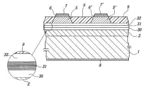
Fig. 3 is a cross sectional view showing a second embodiment
of the optical wavelength converter according to the invention. In this
embodiment, the active layer is formed by the quantum well structure.
In this embodiment, portions similar to those of the previous embodi-
ment are denoted by the same reference numerals used in Figs. 1 and 2.
On the first cladding layer 2, there is :formed a first optical confinement
layer 30 made of InGaAsP (~=1.55 pm) and having a thickness of
200 nm. Next, a quantum well structure layer 31 is formed on the first
optical confinement layer 30, said quantum well structure layer being
constructed by five quantum well layers of InGaAsP (~=1.75 p.m)
having a thickness of 10 nm and five barrier layers of InGaAsP
(~,=1.25 pm) having a thickness of l0:nm, said quantum well layers and
barrier layers being stacked alternately. On the quantum well structure
layer 31, is further formed a second optical confinement layer 32 made
of InGaAsP (~,=1.25 Vim) and having a thickness of 200 nm. It should
be noted that such a quantum well structure has been known in the art,
and a further detailed explanation is dispensed with.
The present invention is not limited to the above explained
embodiments, but many modifications and alternations may be
conceived by a person skilled in the art within the scope of the
invention. The semiconductor optical amplifier may be made of
98144 (10-273,435)
CA 02267018 1999-03-26
_ ] G~ _
various composition semiconductor materials such as GaAIAs/GaAs
series, InGaAIAs/InP series and InGa.As/GaAs series other than
InGaAs/InP series.
Furthermore, in the above embodiments, after forming the two
ridges of the second and third cladding layers 5 and 5', the space
between these ridges is filled with thc~ insulating material, but according
to the invention, the ridges may be formed by selectively converting
portions of the cladding layer into the; electrically insulating areas by
selectively injecting protons into said selected portions.
In the above explanation, the present invention is applied to
the optical wavelength converter. However, the principle of the
present invention may be applied to active directional optical couplers
and optical switching elements, in which the second light wave
impinging upon the first waveguide is selectively transferred into the
second waveguide in dependence upon the first input optical signal.
98144 (10-273,435)