Note: Descriptions are shown in the official language in which they were submitted.
CA 02267076 1999-03-24
WO 98/13882 PCT/EP97/05326
METHOD OF MANUFACTURING A PHOTOVOLTAIC FOIL
The invention is in the field of thin film photovoltaic cells. E.g., amorphous
silicon (i.e., a-Si:H) photovoltaic (PV) cells are known structures which
comprise several layers, usually alternatingly of n-doped, intrinsic, and p-
doped silicon, and which essentially have the ability of generating electric
current from incident light. Given that, e.g., sunlight can thus be used to
generate power, photovoltaic cells form an interesting alternative source of
energy in principle, one much more environment-friendly than fossil fuels or
nuclear power. However, for such PV cells to become a serious and
economically attractive alternative, they need to be provided in a suitable
form and made by relatively low-cost processes, using relatively
inexpensive raw materials.
In order to satisfy this demand, the present invention is directed to a
process by which photovoltaic cells can be made in the form of a foil. It is
not only desirable to have photovoltaic cells in the form of a foil because
such may allow economic production on a large scale (in a "roll-to-roll"
process), but also since flexible substrate based photovoltaic cells will be
more versatile and easier to handle than the more conventional amorphous
silicon PV cells made on glass substrates.
Thus, the invention pertains to a method of manufacturing a photovoltaic
foil supported by a carrier and comprising a plurality of layers which
together have the ability of generating electric current from incident light
(hereinafter referred to as "photovoltaic (PV) layers"), a back-electrode
layer on one side adjacent and parallel to the photovoltaic layers, and a
transparent conductor layer on the other side adjacent and parallel to the
photovoltaic layers, the method comprising providing a substrate, and
applying the transparent electrode layer and the photovoltaic layers
CONFfRMATION COPY
CA 02267076 1999-03-24
WO 98/13882 PCT/EP97/05326
2
(including any additional and/or adjuvant layers) onto the substrate. At
some point, after the photovoltaic layers have been applied, the back-
electrode layer is applied. This does not need to be a transparent electrode
and, in fact, preferably is a reflector for visible light (both for
reflectance and
for conductivity, the back-electrode layer will generally be a metal layer).
For the sake of clarity, it is remarked that in the context of the present
invention the term "back" pertains to the side of the PV foil which upon
eventual use will be facing away from the side on which the light is to fall.
Such a method is known from, e.g., Shinohara et al. First WCPEC; Dec.S-
9, 1994; Hawaii, pages 682ff (~ IEEE), where the substrate used is
polyethylene 2,6- naphthalene dicarboxylate) (PEN). The disclosed
method has several serious drawbacks, e.g., first the PV layers are built up,
and then the transparent conductor. This is a logical consequence of the
substrate not being sufficiently transparent, i.e., it cannot eventually serve
as a window for the transparent conductor layer (which is customary in
amorphous silicon PV cells that are made on glass substrates). However,
the necessary "reverse" order of first applying the PV layers and then the
transparent conductor layer imposes serious limits on the transparent
conductor materials used. E.g., a very favourable transparent electrode
layer is F-doped tin oxide. However, in order for this to have the desired
properties and texture, it should preferably be applied at a temperature of
at least 400°C. Such a high temperature may be devastating to the PV
layers, int.al. as a result of crystallisation, diffusion of the dopants,
and/or
loss of hydrogen. The preferred temperature for the deposition of F-doped
tin oxide also causes the PEN substrates to deteriorate and, therefore, this
layer cannot be deposited prior to the PV layers. Thus, with the use of the
desired application temperature of the transparent electrode any sequence
CA 02267076 2003-12-23
3
of deposition on the PEN substrate would adversely affect the fundamental
ability of the PV foil to generate power.
Hence, a process is required which allows the roll-to-roll manufacture of a
(relatively tough) photovoltaic foil or device, while at the same time making
it
possible to use any desired transparent conductor material and deposition
process, and without jeopardizing the current-generating action of the PV
layers. These requirements, and other desirable objects, are met by the
process of the invention.
To this end, the invention consists of a method of the aforementioned known
type, which method comprises the following subsequent steps:
~ providing a temporary substrate,
~ applying the transparent conductor layer,
~ applying the photovoltaic layers,
~ applying the back-electrode layer
~ applying the (permanent) carrier
~ removing the temporary substrate, and, preferably,
~ applying a top coat on the side of the transparent conductor layer.
In accordance with one aspect of there is a method of manufacturing a
photovoltaic foil supported by a carrier and comprising a plurality of
photovoltaic layers which together have the ability of generating electric
current from incident light, a back-electrode layer on one side adjacent and
parallel to the photovoltaic layers, and a transparent conductor layer on the
other side of, and adjacent and parallel to the photovoltaic layers wherein
the
method comprises the following subsequent steps: providing a temporary
flexible substrate having a thickness of up to about 500 microns, applying the
CA 02267076 2003-12-23
3a
transparent conductor layer, applying the photovoltaic layers, applying the
back-electrode layer, applying the carrier, and removing the temporary
flexible
substrate.
In accordance with another aspect of the invention there is a method of
manufacturing a photovoltaic foil supported by a carrier and comprising a
plurality of photovoltaic layers which together have the ability of generating
electric current from incident light, a back-electrode layer on one side
adjacent
and parallel to the photovoltaic layers, and a transparent conductor layer on
the other side of, and adjacent and parallel to the photovoltaic layers
wherein
the method comprises the following subsequent steps: providing a temporary
flexible substrate, applying the transparent conductor layer at a temperature
higher than the temperature to which the photovoltaic layers are resistant,
applying the photovoltaic layers, applying the back-electrode layer, applying
the carrier, and removing the temporary flexible substrate.
In a preferred embodiment of the invention, the transparent conductor layer is
applied at a temperature higher than the one to which the photovoltaic layers
are resistant (e.g., for a-Si:H, the maximum temperature to which the PV-
layers are resistant is about the same as the deposition temperature of the
said layers. Higher temperatures will cause loss of hydrogen and diffusion of
dopants and impurities, thus forming defects that reduce the efficiency of the
PV-layers).
CA 02267076 1999-03-24
WO 98/13882 PCT/EP97/05326
4
These steps and their sequence essentially make it possible for PV cells to
be produced in the form of a foil, while still maintaining the desired order
of
manufacture that is customary in the case of PV cells produced on glass
substrates (in which case one can start by applying the transparent
conductor since the glass will act as a window for it). Thus, when following
the process of the invention, the substrate can be selected so as to allow
any further process steps (like the high-temperature application of a
transparent conductor layer) without any concerns about its (i.e. the
substrate's) transparency or other properties needed for the functioning of
the eventual PV foil. The temporary substrate is removed after the last of
the photovoltaic layers, the back-electrode layer, and also a permanent
carrier back- substrate have been applied, this in order to have the thin PV
foil supported during as many process steps as possible and to ensure that
the foil exhibits sufficient strength and bending stiffness (preferably
adapted to the intended end product). After removal of the temporary
substrate, the transparent conductor (front-electrode) will generally be
provided with a transparent protective layer, which preferably further adds
to the mechanical properties of the foil and/or the end product.
Although the transparent conductor layer will generally be deposited
directly onto the temporary substrate (sometimes preceded by one or more
extremely thin layers serving as a process aid), it is also possible after
providing the temporary substrate to first apply the eventual protective layer
on the said temporary substrate, and then the transparent conductor layer,
followed by the other layers making up the foil. In this case the protective
layer should, preferably, be made of an inorganic material.
Both the temporary substrate itself and the method to remove it (suitably by
means of dissolving or etching) can be selected by the man skilled in the
CA 02267076 1999-03-24
WO 98/13882 PCT/EP97/05326
art without great difficulty. E.g., the temporary substrate may be a
"positive"
photoresist, i.e., a photosensitive material which upon irradiation undergoes
a change from solvent-resistant to solvent-extractable, e.g., cross-linked
polyimides. In order to meet the object of using low cost materials, these
5 are not the substrates of preferred choice. In this respect it is more
advantageous to use polymers that can be removed by means of plasma
etching (e.g., OZ plasma or, e.g. for polysiloxane polymers, SF6 plasma).
While basically any polymer will thus be suitable, in view of the above it is,
of course, preferred to employ polymers which can withstand higher
temperatures (250°C and more preferably above 400°C).
By preference, the temporary substrate according to the present invention
is a metal or metal alloy foil. The main reason for this is that such foils
generally will be able to withstand the highest temperatures during further
processing, suffer little from evaporation, and can be removed relatively
easily using known etching techniques. Another reason to choose metal,
notably aluminium or copper, is that the PV foil should eventually contain
"side" electrodes {which form a contact for connection to any auxiliary
apparatus or net, i.e., to actually use the PV foil as a source of power). By
allowing part of the temporary substrate to remain in place (e.g., as side
edges or stripes) these contacts do not need to be applied separately.
Suitable metals include steel, aluminium, copper, iron, nickel, silver, zinc,
molybdenum, and alloys or multilayers thereof. Int.al. for economic reasons
it is preferred to employ Fe, AI, Cu, or alloys thereof. For the sake of
performance (combined with costs) aluminium, electrodeposited iron, and
electrodeposited copper enjoy the highest preference. Suitable etching
techniques are known and, while different for each metal chosen, can be
selected by the person skilled in the art using due skill. Preferred etchants
CA 02267076 1999-03-24
WO 98/13882 PCT/EP97/05326
6
include acids (Lewis acids as well as Bra~nstedt acids), e.g., in the case of
copper as a metal foil, it is preferred to use FeCl3, nitric acid, or sulfuric
acid. Aluminium can be efficiently removed by means of, e.g., caustic soda
(NaOH).
For the sake of removability, the temporary substrate preferably is as thin
as possible. Of course it should still allow applying further layers onto it,
and keeping these together, but this generally will not require thicknesses
above 500 pm. Preferably, the thickness is 1 to 200 p,m. Depending on the
modulus of elasticity, a majority of materials will require a minimum
thickness of 5 pm, in which case the preferred range is 5 to 100 um,
preferably 5 to 50 pm, thickness.
The permanent carrier material can be applied over the back-electrode
layer, i.e., "on top" as seen from a process point of view, but in fact on the
eventual back or bottom of the foil. Hence, the new carrier layer will
eventually form a true substrate (the layer denoted "temporary substrate"
during the process in fact is a "superstrate," as it is placed on the eventual
front side or top of the foil). Suitable materials for this carrier layer
include
polymeric foils, such as polyethylene terephthalate, polyethylene 2,6-
naphthalene dicarboxylate), polyvinyl chloride, or high-performance
polymer foils such as aramid or polyimide foils, but also, e.g., metal foils
provided with an insulating (dielectric) top layer, plate glass, or composites
comprising epoxy and glass. Preferred are polymeric "co-extruded" foils
comprising a thermoplastic adhesive layer having a softening point below
that of the carrier itself. Optionally, the co-extruded foil is provided with
an
anti-diffusion layer (for instance, polyester (PET), copolyester, and
aluminium respectively). The thickness of the carrier should preferably lie
within the range of 75 p.m to 10 mm. More preferred ranges are 100 pm to
CA 02267076 1999-03-24
WO 98/I3882 PCT/EP97/05326
7
6 mm and 150 ~m to 300 Vim. The bending stiffness (within the framework
of the present invention being defined as the modulus of elasticity ('E' in
N/mm2) of the material multiplied by the thickness ('t' in mm) of the carrier
cubed: E x t3) preferably is larger than 16x10-2 Nmm and will usually be
smaller than 15x1 O6 Nmm.
The carrier (the eventual substrate) itself may already be, or contain, a
structure required for the intended use. Thus, the carrier may be, e.g., a
tile
or set of tiles, roof tiles, shingles, a car roof, a caravan roof, etc.
However,
in general, it is preferred that the temporary substrate and/or the carrier is
flexible.
As mentioned above, a "top coat" or top layer is applied onto the
transparent conductor. This will generally be a (cavity) plate or polymeric
film having a high transmission, such as amorphous (per)fluorinated
polymers, polycarbonate, poly(methyl methacrylate), or any available clear
coat such as those used in the automotive industry. if so desired, an
additional anti-reflection or anti-pollution layer may be applied.
It is further preferred that the bending stiffness of the foil after the last
process step (which bending stiffness will usually be determined for the
greater part by the carrier and the top coat) is greater than the bending
stiffness of any one of the intermediate products.
It is noted that JP Laid-open no. 1987-123780 concerns a method of
making photo-electric conversion films in which subsequently a TCO
electrode, PV layers, and a further TCO electrode are deposited on a
substrate. The substrate is then removed to give a very thin and highly
flexible film. The addition of a supporting carrier, which is essential to the
CA 02267076 1999-03-24
WO 98/13882 PCT/EP97/05326
8
present invention and which re: ws in a comparatively thick (e.g., 100 ~.m)
and rigid foil, would run counter to the teaching of JP 1987-123780.
Further, although JP 1987-123780 indeed discloses the use of a temporary
substrate, it also proposes consistently and repeatedly to deposit a TCO on
the PV layers. Thus, the use of a temporary substrate does not entail
avoiding either the deposition of a TCO on the PV layers or the detrimental
effects of said deposition on the PV layers.
US 5,232,860 concerns a similar photovoltaic device of exceptional
flexibility which is formed on a plate glass substrate. A lead layer is used
to
promote the detachment of the device from the glass substrate. Again, the
addition of a carrier is not mentioned and would make the desired
"exceptional flexibility" (which is the main objective of the technology of US
5,232,860) impossible and, again, a TCO may be deposited on the PV
layers. A roll-to-roll process is not an option in the manufacture of the
devices of US 5,232,860 because the temporary substrate should be made
of glass or a similar material.
Japanese Laid-open 1980-143706 discloses the use of a removable
substrate for the manufacturing of formed high-polymer products (such as
films and ocellar or ommateal lenses) comprising a transparent electrically
conductive layer. Photovoltaic cells (or products of a similarly complicated
structure) and the problems encountered in such cells are not disclosed in
JP 1980-143706, which publication, accordingly, has no bearing on the
present invention.
EP 189 976 concerns a method for the production of semiconductor
devices (especially solar cells) similar to that of Shinohara et al. In the
CA 02267076 1999-03-24
WO 98/13882 PCT/EP97/05326
9
method according to EP 186 976 first the PV layers are built up and then
the transparent conductor is applied to the PV layers.
Kishi et al., "Ultralight Flexible Amorphous Silicon Solar Celi and Its
' 5 Application for an Airplane," Technical Digest of the International PVSEC-
5,
Kyoto, Japan, 1990, pages 645-648, discloses a solar cell manufactured by
depositing the respective layers on a transparent plastic film. A temporary
substrate is neither mentioned nor implied.
It is preferred that the temporary substrate is an electrodeposited (i.e.,
galvanic) metal layer. Besides allowing the provision of easily removable
thin (< 100 pm) metal layers, this method has considerable advantages,
particularly in respect of the working of the PV foil. Namely, in order for
any
PV cell to operate efficiently, it is desired that incident light be scattered
through the PV structure as much as possible. To this end, the PV cell's
surface, as well as the other layers', needs a certain texture, e.g., such
that
the surface comprises a plurality of optical prisms (which lead to incident
light breaking and spreading through the PV cell). A great advantage of
galvanically providing metal foil is that the galvanic (electrodeposition)
process makes it possible to give the foil any desired texture. This texture
can be obtained by texturing the surface (usually a drum) on which the
metal is electrodeposited. When the PV foil is built up on a textured
substrate, the substrate works as a mould, imposing on its adjacent layer,
and the subsequent layers, the negative image of said texture (conformal
coating). The desired drum surface can be attained in a manner known in
itself, e.g., by laser engraving or by any photolithographic process. It is
also
possible to generate a textured surface on the side facing away from the
drum. The texture at this side is not or not only affected by the surtace
texture of the drum and the material of which the drum is made, but also by
CA 02267076 1999-03-24
WO 98/13882 PCT/EP97I05326
such process parameters as the current density, the choice and
concentration of the electrolyte employed, and by any additives used. The
man skilled in the art knows how to adjust the relevant parameters and will
be able to attain surface roughnesses of the order of 0.1 to 10 ~m
5 (perpendicular to the surface, RZ).
While a scattering texture is preferred, more preferred is a texture
comprising a plurality of adjacent pyramids, thus having alternating
protrusions and indentations, the relative distance between which (RZ)
10 preferably is of the above order, and more preferably approximately 0.15 or
0.2 pm. It is further preferred that the protrusions and indentations have a
rounded shape (e.g., an angle of basis to hypotenuse of maximally 40°),
in
order to prevent possible defects in the amorphous silicon layers which
may occur in the case of sharp peaks or sharp valleys. It is to be
understood that if protruding pyramids are present on the surface of the
drum or the like, the negative image thereof imposed on the temporary
substrate and eventually on the transparent conductor and other layers will
be a reverse pyramidal structure, having indentations rather than
protrusions of pyramidal shape. Hence, by adjusting the texture of the
temporary substrate the invention essentially allows the texture of the
transparent conductor to be tuned in such a way as to eventually give it
optimal surface morphology.
in view of the possibility of influencing the eventual texture, it is desired
to
choose copper for the electrodeposited metal foil. However, as copper may
have the tendency to diffuse through the silicon PV layers, it is preferred to
provide the copper foil (galvanically) with a non-reducing diffusion barrier,
e.g., an anti-corrosion layer, notably zinc oxide, or to select a transparant
conductor which has the ability to prevent said diffusion, e.g., Ti02, AI203,
CA 02267076 1999-03-24
WO 98/13882 PCT/EP97/05326
11
Sn02, or ZnO. The anti-diffusion layers can be applied, e.g., galvanically by
Physical Vapour Deposition (PVD) or by Chemical Vapour Deposition
(CVD).
' S Instead of the copper foil being provided with an anti-diffusion layer,
which,
as a rule, will be removed with the temporary substrate, it is also possible
to provide the copper foil (or any other temporary substrate chosen) with a
layer of a suitable kind of glass. This glass layer essentially is
transparent,
and can thus be permanent, serving as a protective window for the
transparent conductor layer. For reasons of economy, and to allow roll-to-
roll processing, the glass layer preferably is very thin, e.g. 100 to 200 nm
thickness. A suitable application method for such a layer, e.g., is PECVD
{Plasma Enhanced Chemical Vapour Deposition) of SiH4 and N20 (plasma
oxide) and adding a suitable additive such as B2H6 to form a boron-silicate
glass having a favourable transparency. It is preferred to apply APCVD
silicon oxide.
After the temporary substrate has been provided in this manner, the layers
actually making up the PV cells (in the form of a foil) can be provided.
Broadly speaking, a PV cell of the thin film semiconductor type comprises a
transparent conductor (which will eventually form the "front side" of the
foil,
i.e., the side which in use is to be irradiated with (sun)light), a plurality
of
thin film semiconductor layers which together exhibit a photovoltaic effect,
such as a stack of p-doped, intrinsic, and n-doped amorphous silicon
layers, and the back-electrode layer mentioned earlier, which preferably
also serves as a reflector. Both the front side and the back can be provided
with any desired protective layers, the main requirement for the front side
being, of course, that such a layer is transparent, and further desired
properties including good adhesion, wear, weather, and UV resistance, etc.
CA 02267076 1999-03-24
WO 98/13882 PCT/EP97/05326
12
The transparent conductor (usually TCO - transparent conductive oxide)
can be deposited in a known manner, e.g., using Metal Organic Chemical
Vapour Deposition (MOCVD), sputtering, Atmospheric Pressure Chemical
Vapour Deposition (APCVD), PECVD, spray pyrofysis, evaporation
(physical vapour deposition), electrodeposition, screen printing, sol-gel
processing, etc. It is preferred that the transparent conductor layer is
applied at a temperature higher than 250°C, preferably higher than
400°C,
so as to make it possible to obtain a transparent conductor layer having
advantageous properties and/or texture.
Examples of materials suitable for use in the transparent conductor layer
are indium tin oxide, zinc oxide, aluminium- or boron-doped zinc oxide,
cadmium sulfide, cadmium oxide, tin oxide and, most preferably, F-doped
Sn02. This last transparent electrode material is preferred for its ability to
form a desired crystalline surface having a columnar, light-scattering
texture if applied at a temperature well above 400°C, preferably
500°C to
600°C. Particularly with this electrode material, the advantages of
selecting
a temporary substrate (which allows said high temperature) and, more
particularly, selecting a textured electrodeposited metal substrate, are
exhibited to a great extent. Further, the material has the advantage of
being resistant to the most preferred etchants used, as well as having
better chemical resistance and better opto-electronic properties than indium
tin oxide. Besides, it is much less expensive.
After application of the transparent conductor layer, the PV foil can be built
up as desired. It is known how to apply PV layers and also which layer
configurations to choose. For the common general knowledge on this point
reference is made to Yukinoro Kuwano, "Photovoltaic Cells," Ullmann's
CA 02267076 1999-03-24
WO 98/13882 PCT/EP97/05326
13
Encyclopedia, Vol.A20 (1992), 161, and to "Solar Technology," Ullmann's
Encyclopedia, VoLA24 (1993), 369.
Various thin film semiconductor materials can be used to make up the PV
layers. Thus the required PV cells can be made from amorphous silicon (a-
Si:H), microcrystalline silicon, polycrystalline amorphous silicon carbide (a-
SiC) and a-SiC:H, amorphous silicon-germanium (a-Site) and a-SiGe:H.
Further, the PV foils of the invention may comprise C1S PV cells (copper
indium diselenide, CuinSe2), cadmium telluride cells, Cu(In,Ga)Se cells,
ZnSe/CIS cells, Zn0/CIS cells, Mo/CIS/CdS/Zn0 cells.
In the preferred case of amorphous silicon cells comprising a fluorine-
doped tin oxide, these will generally comprise a stack, or a plurality of
stacks, of p-doped, intrinsic, and n-doped amorphous silicon layers, with
the p-doped layers being situated on the side facing the incident light.
Thus, in the a-Si-H embodiment, the PV layers will at least comprise a p-
doped amorphous silicon layer (Si-p), an intrinsic amorphous silicon layer
(Si-i), and an n-doped amorphous silicon layer (Si-n). It may be that onto
the first set of p-i-n layers a second and further p-i-n layers are applied.
Also, a plurality of repetitive p-i-n ("pinpinpin" or "pinpinpinpin") layers
can
be applied consecutively. By stacking a plurality of p-i-n layers, the voltage
per cell is raised and the stabilized efficiency is increased (light-induced
degradation, the so-called Staebler-Wronski effect, is diminished).
Furthermore, the spectral response can be optimized by choosing different
band-gap materials in the various layers, mainly the i-layers, and
particularly within the i-layers. The overall thickness of all the a-Si layers
together will generally be of the order of 100 to 2000 nm, more typically
about 200 to 600 nm, and preferably about 300 to 500 nm.
CA 02267076 1999-03-24
WO 98/13882 PCT/EP97/05326
14
In order for the PV foil to be able to function properly in the various
layers,
in various positions, it is preferred that material be partially removed to
create separated stripes of 5 to 100 mm, preferably about 5-25 mm, in
order to provide the required electrically conductive through-connections for
the PV cells in the foil to be in series (each p-i-n yields about 0.5 V at the
maximum power point, and a plurality of p-i-n cells will generally be put in
series to generate the desired voltage of a foil). This can be done in a
known manner using a laser. Alternatively, it is also possible to employ
(chemical) etching techniques to this end. In order to avoid the normally
required number of process steps (coating of a photoresist, irradiating it
through a mask, developing it, etching, rinsing, and stripping of the resist),
the present invention provides a simple manufacturing tool which will
eventually give the desired etching pattern. To this end, the invention in
one embodiment provides a patterned coating of a thin layer of etchant on
each layer. That this is possible results from the recognition that the layers
in which etching is to be carried out are relatively thin, which will allow
applying etchant-containing substances in a sufficient amount for etching to
occur. While a typical thickness for each layer in the foil is of the order of
a
hundred to several hundreds of nm, the layers of etchant can be applied in
thicknesses of, e.g., 25 ~m (= 25000 nm) length and width. Since the
different layers have different resistivity against etchants, it is possible
for
the eventual foil to contain several stripes of different etchants in the
different layers. The required small stripes can be applied onto each layer
during (roll-to-roll) processing of the PV foil. Suitable application
techniques
include flexo-gravure, rotation screen printing, ink jet, extrusion coating,
transfer coating, etc. In other words, in each process step, after the
application of each layer of which parts should be removed, etchant is so
applied. Onto a layer of F-doped Sn02, e.g., one applies a strong base
such as KOH. The etching process can be accelerated by heating, which
CA 02267076 1999-03-24
WO 98/13882 PCT/EP97105326
therefore may be an additional process step. Ai-doped Zn0 can be
removed, e.g., by using an acidic etchant, such as sulfuric acid. Other
transparent electrode materials can be etched away using the appropriate
etchants generally known to the skilled man (e.g., indium tin oxide can be
' S etched using KOH). Amorphous silicon can be etched using strong base
such as NaOH or KOH. The back-electrode can be etched using acid.
Essentially, all etching steps can be conducted using the same apparatus,
or set of stations, in which after allowing sufficient etching time the etched
10 layer is washed/rinsed and dried. Since the process is conducted on a
flexible (temporary) substrate, in each step of the entire manufacturing
process there is question of a self-sustaining foil which can be led through
various treatment stations (such as baths) by unwinding, and collected by
rewinding. Although for this reason it is preferred to carry out all the
etching
15 steps when the temporary substrate is present, it is possible to partially
remove the transparent conductor after removal of the temporary substrate.
It should be noted that, in principle, the above etching method is universally
applicable to all processes in which thin film, e.g., amorphous silicon, PV
cells or foils are produced.
The stripes of etchant preferably are as narrow as possible, e.g., 1 to 50
Vim, and preferably 20-25 ~m or smaller, as at the site of these stripes the
PV foil does not have current-generating activity.
After the active amorphous silicon layers have been applied, the PV foil is
provided with the aforementioned back-electrode layer, which preferably
can serve simultaneously as a reflector and as an electrode layer (i.e., as
this eventually will be the "back" electrode, the transparent conductor layer
CA 02267076 1999-03-24
WO 98/13882 PCT/EP97/05326
16
will be a "front" electrode). This back-electrode layer will generally be of
about 50 to 500 nm thickness and may be made up of any suitable material
having light-reflecting properties, preferably aluminium, silver, or a
combination of layers of both. These metal layers can be applied
(preferably at a relatively low temperature, e.g., lower than 250 °C)
by
means of (in vacuo) physical vapour deposition (evaporation) or sputtering,
optionally using a mask to prevent deposition at sites where stripes need to
be etched or by use of masking wires. In the case of silver, it is preferred
to
first apply an adhesion promotion layer, for which, e.g., Ti02 and Zn0 are
suitable materials and have the advantage of additionally being reflecting if
applied in a suitable thickness (e.g. about 80 nm).
Like the layers applied previously, the back-electrode layers are made to
contain "stripes," i.e. directly adjacent and parallel to the already existing
stripes, narrow tracks of the reflector layer are removed. Again, this
removal of material can be carried out using several techniques, such as
laser scribing, wet chemical etching, plasma etching, or by "direct etch
coating," i.e. the aformentioned deposition of etchant in preformed tracks.
The etching of stripes from this "back electrode" serves to provide the
necessary series connection for the individual PV cell created in the foil.
The above-indicated etching techniques can be applied in the subsequent
removal of the temporary substrate. E.g., the foil is passed through an
etching bath comprising a strong base or H2S04 or FeCl3, or such
Bra~nstedt or Lewis acids are coated or sprayed onto the metal foil forming
the temporary substrate. The removal of the substrate is followed by
conventional rinsing and drying steps. If it is desired to only remove part of
the temporary substrate (i.e. only at those parts of the surface where
incident light needs to reach the transparent conductor), before etching an
CA 02267076 1999-03-24
WO 98/13882 PCT/EP97/05326
17
"etch resist" may be applied, preferably in narrow stripes at most covering
two transparent conductor tracks.
Thus a ready-to-use PV foil is provided on a roll. If desired, sheets having a
' S predetermined power and voltage can be cut from the foil.
In accordance with the above described technology, the invention further
pertains to a method of manufacturing a thin film photovoltaic foil
comprising as subsequent layers: a back-electrode layer, a plurality of
photovoltaic layers, and a transparent conductor layer, the top electrodes
and the back electrodes being connected in series, in which method tracks
are defined in the back electrode prior to the application of the carrier and
tracks are defined in the transparent conductive layer after the deposition
of the photovoltaic layers and the back electrode and, preferably, after
removal of the temporary substrate. It is further preferred that the tracks
are
defined preferably by laser scribing or etching. In the case of etching, it is
preferred that a patterned coating of a thin layer of etchant is provided on
the back electrode and/or the transparent conductive layer.
Without the following being intended as limiting the invention, by way of
example a description is given of making a PV foil in accordance with the
invention, with reference to the drawings. All figures depict a cross-section,
at several stages of the manufacturing process, of one and the same
portion of foil in the longitudinal (production) direction.
FIG. 1: a temporary substrate (1 ) in the form of a metal foil such as
aluminium is provided.
CA 02267076 1999-03-24
WO 98/13882 PCT/EP97/05326
18
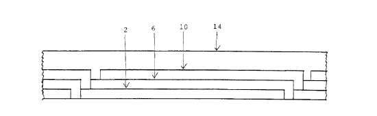
FIG. 2: a transparent conductor (2) is deposited onto the metal foil (1),
e.g.,
a layer of F-doped Sn02 of about 600 nm thickness applied by means of
APCVD at approximately 550°C. Optionally, before the PV layers are
applied, a Zn0 intermediate layer (about 80 nm thickness) is deposited
onto the transparent conductor layer (not shown).
FIG. 3 and FIG.4: the transparent conductor layer (2) is partially removed
by means of laser scribing or by etching lines (3). The remaining parts are
stripes (4) of about 20 mm width separated by narrow tracks (about 25 Vim)
of removed material (5).
FIG. 5: the PV layers (6) are applied. These will comprise one or more sets
of a p-doped amorphous silicon layer (Si-p), an intrinsic amorphous silicon
layer (Si-i), and an n-doped amorphous silicon layer (Si-n), in an overall
thickness of approximately 500 nm (not individually shown).
FIGS. 6 and 7: the amorphous silicon layers (6) are provided with a pattern
of stripes (7) by removing narrow tracks of material by means of laser
scribing or by applying chemical etchant (8). The tracks of removed
material (9) are applied as close as possible to the removed tracks (5) in
the transparent conductor layer.
FIGS. 8 to 10: an aluminium layer (10) of approximately 250 nm thickness
is applied onto the amorphous silicon layers (6) to serve simultaneously as
a back-electrode and a reflector layer and provided with stripes (11) by
etching away material in tracks (12) directly adjacent and parallel to those
generated previously (9), possibly by first applying etchant (13).
CA 02267076 1999-03-24
WO 98/13882 PCT/EP97/05326
19
FIGS. 11 and 12: a carrier (14) is applied onto the back electrode (10), after
which the metal foil temporary substrate (1) is removed (by etching). The
carrier (14) in use will be the actual substrate (back, bottom) of the PV foil
made in accordance with the invention.
FIG. 13: the eventual front side comprising the transparent conductor layer
(2) is provided with a protective clear top coat (15).
In a further example according to the invention, the production of a
cadmium telluride thin film solar cell is described. An aluminium temporary
substrate was provided on which a layer of Sn02: F was coated by means
of APCVD at a temperature of 550°C. Next, a layer of CdS (thickness:
100
nm) was applied and subsequently annealed at 400°C in an H2
atmosphere. After annealing the assembly was heated to 550°C, and
cadmium and tellurium were deposited on the CdS layer using a so-called
closed space sublimation process in an He and 02 atmosphere (source to
substrate distance 5 mm, the CdTe source was heated to 650°C and the
substrate to 550°C, both in an H2 and 02 atmosphere with a partial
pressure of both gasses of 30 Torr). The assembly was then treated with
CdCl2 vapour at 425°C, followed by sputtering a back contact.
Finally, the
temporary substrate was removed by etching using an NaOH solution.
Besides pertaining to a method, the present invention also includes novel
PV products, int. al., a photovoltaic foil comprising, as subsequent layers: a
reflecting electrode layer, a plurality of photovoltaic layers, and a
transparent conductor layer, with the foil, faced from the side of the
transparent conductor layer, having a surface texture of indented, inverse
pyramids.
CA 02267076 1999-03-24
WO 98/13882 PCT/EP97/05326
Further, by virtue of the above manufacturing method involving the use of a
temporary substrate, the present invention allows for substantial
improvement of PV cells of the flexible, foil type. Thus, the invention also
pertains to a photovoltaic foil comprising, as subsequent layers, a reflecting
5 electrode layer, a plurality of photovoltaic layers, a transparent conductor
layer, and a transparent protective coating, the improvement consisting in
that the transparent conductor layer is fluorine-doped tin oxide. While this
is
a conductor known in itself, and highly desirable for PV cells, the state of
the art processes do not allow it to be employed as the transparent
10 conductor in PV foils. I.e., the present invention is the first to achieve
a PV
structure of the type having F-doped Sn02 with the desired properties as a
transparent conductor (and deposited at a temperature above 400°C) in
the
form of a flexible foil.
15 In fact, the present invention provides a PV material which may have an F-
Sn02, or other transparent conductor applied at high temperature, without
this conductor layer necessarily being covered with a plate-glass window
(which is the state of the art for PV cells having these transparent
conductors).