Note: Descriptions are shown in the official language in which they were submitted.
CA 02267293 1999-03-30
WO 98/15991 PCT/US97/18354
1
HIGH DENSITY CONNECTOR AND
METHOD OF MANUFACTURE
Background of the Invention
1. Field of the Invention: The present invention relates to
electrical connectors and more particularly high I/O density connectors,
such as array connectors.
2. Brief Description of Prior Developments~ The drive to reduce
the size of electronic equipment, particularly personal portable devices,
and to add additional functions to such equipment, has resulted in an
ongoing drive for miniaturization of all components, especially electrical
connectors. Efforts to miniaturize connectors have included reducing the
pitch between terminals in single or double row linear connectors, so that
a relatively high number of I/O or other lines can be interconnected by
connectors that fit within tightly circumscribed areas on the circuit
substrates allotted for receiving connectors. The drive for miniaturization
has also been accompanied by a shift in preference to surface mount
techniques (SMT) for mounting components on circuit boards. The
confluence of the increasing use of SMT and the required fine pitch of
linear connectors has resulted in approaching the limits of SMT for high
volume, low cost operations. Reducing the pitch of the terminals
increases the risk of bridging adjacent solder pads or terminals during
reflow of the solder paste. To satisfy the need for increased I/O density,
CA 02267293 1999-03-30
WO 98/I5991 PCT/US97/18354
2
array connectors have been proposed. Such connectors have a two
dimensional array of terminals mounted on an insulative substrate and
can provide improved density. However, these connectors present certain
difficulties with respect to attachment to the circuit substrates by SMT
techniques because the surface mount tails of most, if not all, of the
terminals must be beneath the connector body. As a result, the mounting
techniques used must be highly reliable because it is difficult to visually
inspect the solder connections or repair them, if faulty. In the mounting
of an integrated circuit (IC) on a plastic or ceramic substrate the use of
ball grid array (BGA) and other similar packages has become common. In
a BGA package, spherical solder balls attached to the IC package are
positioned on electrical contact pads of a circuit substrate to which a
layer of solder paste has been applied, typically by use of a screen or
mask. The unit is then heated to a temperature at which the solder
paste and at least a portion or all of the solder ball melt and fuse to an
underlying conductive pad formed on the circuit substrate. The IC is
thereby connected to the substrate without need of external leads on the
IC.
While the use of BGA and similar systems in connecting an IC to a
substrate has many advantages, a corresponding means for mounting an
electrical connector or similar component on a printed wiring board (PWB)
or other substrate has yet to be developed. It is important for most
CA 02267293 1999-03-30
WO 98/15991 PCT/US97/18354
3
situations that the substrate-engaging surfaces of the solder balls are
coplanar to form a substantially flat mounting interface, so that in the
final application the balls will reflow and solder evenly to a planar printed
circuit board substrate. Any significant differences in solder coplanarity
on a given substrate can cause poor soldering performance when the
connector is reflowed onto a printed circuit board. To achieve high
soldering reliability, users specify very tight coplanarity requirements,
usually on the order of 0.004 inches. Coplanarity of the solder balls is
influenced by the size of the solder ball and its positioning on the
connector. The final size of the ball is dependent on the total volume of
solder initially available in both the solder paste and the solder balls. In
applying solder balls to a connector contact, this consideration presents
particular challenges because variations in the volume of the connector
contact received within the solder mass affect the potential variability of
the size of the solder mass and therefore the coplanarity of the solder
balls on the connector along the mounting interface.
Another problem presented in soldering connectors to a substrate is
that connectors often have insulative housings which have relatively
complex shapes, for example, ones having numerous cavities. Residual
stresses in such thermoplastic housings can result from the molding
process, from the build up of stress as a result of contact insertion or a
combination of both. These housings may become warped or twisted
CA 02267293 1999-03-30
WO 98!15991 PCT/US97/18354
4
either initially or upon heating to temperatures necessary in SMT
processes, such as temperatures necessary to reflow the solder balls.
Such warping or twisting of the housing can cause a dimensional
mismatch between the connector assembly and the PWB, resulting in
unreliable soldering because the surface mounting elements, such as
spider balls, are not sufficiently in contact with the solder paste or close
to the .PWB prior to soldering.
A need, therefore, exists for reliably and efficiently mounting high
density electrical connectors on substrates by surface mounting
techniques.
Summary of the Invention
Electrical connectors according to the present invention provide
high I/O density and reliable attachment to circuit substrates by SMT
techniques. These connectors exhibit high coplanarity along the
mounting interface.
Electrical connectors of the present invention are ones in which
one or more terminals are connectable by a fusible electrically conductive
material to a substrate. This fusible electrically conductive material is a
solder mass, preferably comprising a solder ball that can be reflowed to
provide the primary electrical current path between the terminal and a
circuit substrate.
CA 02267293 1999-03-30
WO 98/15991 PCT/US97/18354
An aspect of the invention includes methods for forming an exterior
fusible conductive contact on an element of an electrical connector.
According to one method, a recess is formed on the exterior side of the
connector elements or contacts. A section of a conductive contact extends
5 from adjacent the interior side of the conductor element into the recess on
the exterior side of the housing. The recess is filled with a controlled
volume of solder paste. A fusible conductive elerrient, for example a solder
ball, is positioned in the recess on the exterior side of the housing. The
conductive element placed in the recess is then heated .to a temperature
sufficient to fuse the solder paste and fuse the fusible conductive element
to the section of the contact extending into said recess.
Also encompassed by this invention is a contact for use in an
electrical connector which comprises a terminal tab area where said
contact is connectable to a fusible conductive element, such as a solder
ball. A medial area of the contact is positioned between the terminal tab
and a contact area. The medial area is adapted to resist molten solder
flow, for example, by application of a coating or plating of a non-solder
wettable material. By this arrangement wicking of the solder from the
solder ball from the area of attachment to the contact avoided.
Coplanarity of the surface mounting interface of the connector is
maintained by providing an insulative connector housing in which stress
buildup is avoided. According to this aspect of the invention, a contact
terminal is inserted into an opening in the housing. The cross section of
CA 02267293 2002-02-20
6
the opening is configured so that at least one side thereof has or comprises a
shaped projection adapted to be deformed by the terminals as the terminal is
inserted into the opening. >3y means of this arrangement, stress build up as a
result of multiple contact insertions is avoided, so as to minimize warping
and twisting of the housing.
In accordance with one aspect of the present invention there is
provided an electrical connec~:or adapted to be mounted on a substrate having
a conductive element, comprising:
a contact having a connector portion adapted to be electrically
connected to said conductive element;
a body of reflowable, electrically conductive material disposed on the
connector portion, said body being adapted to provide the primary
electrical current path between the connector and the substrate.
In accordance with another aspect of the present invention there is
provided an electrical connector adapted to be mounted on a substrate having
a conductive element, comlarising:
an insulative housing, the housing having an exterior side adapted to
face the substrate;
a contact, the contact having a corulection portion adapted to be
electrically connected to said conductive element; and
a body of reflowable, electrically conductive material disposed on the
connection portion adjacent said the exterior side of the housing.
In accordance with another aspect of the present invention there is
provided an electrical connector comprising: an insulative housing having a
base wall with an interior side and an exterior side, a plurality of recesses
on
said exterior side; a plurality of contact receiving slots, each of said slots
extending from the interior side of said base wall to one of said recesses; a
contact disposed in each of said slots, a plurality of bodies of reflowable,
CA 02267293 2002-02-20
6a
electrically conductive material, each body being associated with a recess and
having a portion thereof disposed in the recess and fused to the contact.
In accordance with another aspect of the present invention there is
provided an electrical connector comprising:
an insulative member having a contact bearing side and a mounting
side;
an electrical terminal mounted on the insulative member, the terminal
having a contact portic;m disposed on the contact bearing side of the
insulative member and a mounting portion, the mounting portion
having a securing section extending at least partially through the
insulative member; and
an electrically conductive heat fusible secaion extending from the
securing section to an exterior face on the mounting side of the
insulative body.
In accordance with another aspect of the present invention there is
provided an electrical component adapted to be surface mounted on a circuit
substrate, comprising:
a body formed of an insulative material, the body having a mounting
surface adapted to be disposed in facing relationship to the circuit
substrate and an opening therein extending toward said mounting
surface;
an electrically conductive member mounted on the body, the
conductive member including a terminal portion extending into the
opening toward the mounting surface, and
a securing portion extending from tile terminal portion to the
mounting surface for establishing electrical continuity between the
circuit substrate
and the conductive member, said securing portion including a heat
fusible section.
CA 02267293 2002-02-20
6b
In accordance with another aspect of the present invention there is
provided an electrical connector comprising:
a mounting interface for mounting the connector on a substrate and a
mating interface for presenting electrical contacts for engagement with
contacts of a mating connector;
a plurality contacts mounted on the insulative body; and
a reflowable element secured on each of the contacts and extending
from the contact toward the mounting interface.
In accordance with another aspect of the present invention there is
provided an electrical connector comprising:
an insulative housing having a mating interface for mating with a
mating connector and a mounting interface for mounting on a
substrate including cc:mductive elements;
a plurality of contacts mounted on the housing, each contact having a
mating portion adapted for engaging a contact from the mating
connector and a connector portion adapted to be secured to a
conductive element on the substrate, and
a plurality of solder balls, each solder ball secured on a connection
portion of one of said contacts.
In accordance with another aspect of the present invention there is
provided an electrical connector comprising:
an insulative base;
a plurality of contacts mounted on the base; and
a plurality of solder balls, each solder ball being secured on at least one
of the contacts and fo ming a mounting interface for mounting the
connector on a substrate.
In accordance with another aspect of the present invention there is
provided an electrical connector comprising:
an insulative base;
CA 02267293 2002-02-20
6C
a plurality of contacts mounted on the base; and
a plurality of conductive elements having substrate engaging surfaces,
each conductive element being secured on at least one of the contacts,
the substrate engaging surfaces forming a mounting interface for
mounting the connector on a substrate.
In accordance with another aspect of the present invention there is
provided a method for placing an exterior conductive contact on an electrical
connector having a base forming an exterior side and an interior side
comprising the steps of:
'.!0 providing at least one recess on the exterior side of the base;
providing a conductive contact extending form adjacent the interior
side of the conductor element to the recess on the exterior side of the
base;
positioning a conductive element with at least a portion thereof in the
recess provided on the exterior side of the base; and
securing the conductive element onto the contact while the conductive
element is positioned ~~t the recess.
In accordance with another aspect of the present invention there is
provided a method of making an electrical connector comprising:
mounting a contact teorninal on one surface of an insulative member
with a portion of the terminal extending into the insulative member
toward a second surface of the insulative member; and
securing a fusible electrically conductive body to the portion of the
terminal extending toward the second surface.
In accordance with another aspect of the present invention there is
provided an electrical connector having a base with an exterior side and an
interior side and made by steps comprisinf;:
providing at least one recess on the exterior side of the base;
CA 02267293 2002-02-20
nd
providing a conductive contact extending form adjacent the interior
side of the conductor element to the recess on the exterior side of the
base;
positioning a conductive element with at least a portion thereof in the
recess provided on the exterior side of the base; and
securing the conductive element onto the contact while the conductive
element is positioned a t the recess.
In accordance with another aspect of the present invention there is
provided a method of making an electrical connector comprising:
mounting a contact terminal on one surface of an insulative member
with a portion of the terminal extending into the insulative member
toward a second surface of the insulative member; and
securing a fusible electrically conductive body to the portion of the
terminal extending to~n~ard the second surface.
7.5 In accordance with another aspect of the present invention there is
provided a method of making an electrical connector comprising:
mounting a contact terminal on one surface of an insulative member
with a portion of the terminal extending into the insulative member
toward a second surface of the insulative member; and
:~0 securing a substantialha spherical electrically conductive member to the
portion of the terminal extending toward the second surface.
In accordance with another aspect of the present invention there is
provided an electrical connector comprising:
a connector body;
:?5 at least one contact receiving opening for receiving a portion of a
contact mountable o:n i:he connector body, the opening having a side
wall portion; and
CA 02267293 2002-02-20
6e
a deformable member located adjacent said side wall and adapted to
be deformed by a contact inserted into the opening and secure the
contact in the opening.
In accordance with another aspect of the present invention there is
provided contact for an electrical connector comprising:
a medial portion;
a contact engaging portion extending from the medial portion, said
contact engaging portion being adapted to engage a mating contact;
a solder terminal portion extending from the medial portion and
7.0 adapted to receive solder to be fused thereon; and
said medial section having a coating thereon for resisting solder
wicking from the terminal portion to the engaging portion, the coating
comprising a layer of nickel.
Brief Descr~tion of the Drawings
The method and connector of the present invention is further described
with reference to the accompanying drawings in which:
Fig.1 is a top plan view of a receptacle connector of a preferred
embodiment of the connector of the present invention;
Fig. 2 is a partially ciat away end view of the receptacle shown in Fig. 1;
:Z0 Fig. 3 is a top plan view of a plug element of a preferred embodiment
of the present invention;
Fig. 4 is a partially cut away end view of the plug element shown in
Fig. 3;
Fig. 5 is a cut away end view of the receptacle and plug shown in Figs.
Z5 1 - 4 in unmated relation;
Fig. 6 is an end view o the receptacle and plug shown in Fig. 5 in
mated relation;
CA 02267293 2002-02-20
6f
Figs. 7a, 7b and 7c are cut away end views showing respectively first,
second and third sequential stages in the mating of the receptacle end
plug shown in Fig. 5;
CA 02267293 1999-03-30
WO 98/15991 PCT/US97/18354
7
Fig. 8 is a bottom plan view of the receptacle shown in Fig. 1 before
the placement of solder balls thereon;
Fig. 9 is a bottom plan view of the receptacle shown in Fig. 8 after
placement of the solder balls thereon;
Fig. 10 is a detailed cut away view of area XII in Fig. 1;
Fig. 11 is an enlarged view of the cut away area in Fig. 4;
Fig. 12 is an enlarged view of the cut away area in Fig. 10;
Fig. 13 is an enlarged cross sectional view through 13 - 13 in Fig.
10;
Fig. 14 is a top plan view of a second preferred embodiment of a
receptacle connector of the present invention;
Fig. 15 is an end view of the receptacle shown in Fig. 14;
Fig. 16 is a top plan view of a second preferred embodiment of a
plug connector of the present invention;
Fig. 17 is an end view of the plug shown in Fig. 16;
Fig. 18 is an end view of the mated receptacle and plug shown in
Figs. 14 - 17;
Fig. 19 is a top plan view of a receptacle used in a third preferred
embodiment of a receptacle connector of the present invention;
Fig. 20 is an end view of the receptacle shown in Fig. 14;
Fig. 21 is a top plan view of the plug element of the third preferred
embodiment of a plug connector of the present invention;
CA 02267293 1999-03-30
WO 98/15991 PCTlUS97/18354
8
Fig. 22 is an end view of the plug element shown in Fig. 2;
Fig. 23 is an end view of the mated receptacle and plug shown in
Figs. 19 - 22;
Fig. 24 is a side cross sectional view in fragment of another
embodiment of a connector according to the present invention;
Fig. 24a is a fragmentary view of a portion of the structure of Fig.
24 modified to form a deeper recess;
Fig. 25 is a front cross sectional view in fragment of the connector
shown in Fig. 24 in which the plug and receptacle are unmated;
Figs. 26a and 26b is a graph showing temperature versus time and
distance during solder reflow in Examples 1 and 2 of the method of
the present invention;
Figs. 27a - 27f are laser generated profiles of the product of
Example 3 of the method of the present invention;
Figs. 28a and 28b are x-ray photographs showing the product of
Example 4 of the method of the present invention;
Figs. 28c and 28d are electron microscope photographs showing the
product of Example 4 of the method of the present invention.
Fig. 29 is a view similar to Fig. 10 in which the ground and power
contacts have been omitted;
Fig. 30 is a cross sectional view through XXXI - XXXI in Fig. 13;
CA 02267293 1999-03-30
WO 98/15991 PCT/US97/18354
9
Fig. 31 is a computer generated representation of predicted stresses
in an insulative housing similar to those illustrated in the preferred
embodiments of the present invention;
Fig: 32 is a graph of contact retention force as a function of the
amount of deformation (compression) in a rib of the insulative
housing as is shown in Fig. 29;
Fig. 33 is a front elevational view of a receptacle signal contact used
in a preferred embodiment of the connector of the present
invention;
Fig. 34 is a front elevational view of a plug signal contact used in a
preferred embodiment of the connector of the present invention;
Fig. 35 is a front elevational view of a receptacle ground/power
contact with carrier strip used in a preferred embodiment of the
connector of the present invention; and
Fig. 36 is a front elevational view of a plug ground/power contact
with carrier strip used in a preferred embodiment of the connector
of the present invention.
Detailed Description of the Preferred Embodiments
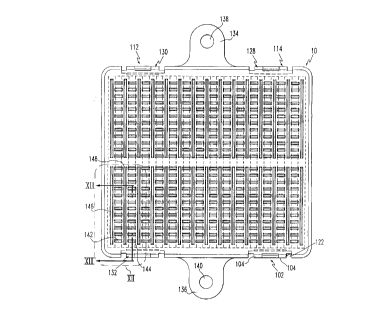
Referring generally to Figs. 1 - 2 and 12 - 13, a set of intermating
connectors according to a first embodiment of a high density connector of
the present invention includes a receptacle which is shown generally at
numeral 10. A base section of the receptacle is shown generally at
CA 02267293 1999-03-30
WO 98/15991 PCT/US97118354
numeral 12. The base is preferably formed by molding an appropriate
insulating polymeric material capable of withstanding SMT reflow
temperatures, for example, liquid crystal polymer (LCP). Referring first to
the base section, this element includes a base wall 14 having an exterior
5 side I6 and an interior side I8. On the exterior side there are outer
recesses as, for example, recesses 20, 22, 24, 26 and 28 (Fig. 12). On the
interior side there are inner contact receiving recesses as, for example,
recesses 30, 32, 34, 36 and 38. Connecting these inner and outer
recesses are medial slots as, for example, slots 40, 42, 44, 46 and 48.
10 Each of the outer recesses has a base wall and a lateral wall as, for
example, base wall 50 and lateral wall 52 (Fig. 12). Each of the inner
signal contact receiving recesses has a base wall and intersecting lateral
walls as, for example, base wall 54 and lateral walls 56 and 58. Each of
the inner ground or power contact receiving recesses also has a base wall
and diagonal lateral walls as, for example, base wall 60 and lateral walls
62 and 64. The above described inner and outer recesses and connecting
medial slots receive ground/ power contacts or signal contacts.
The ground or power contacts preferably have an upper section,
shown generally at numeral 66, formed of two contacting forks 68 and 70.
Each of these forks has a converging section 72, a contact point 74 and
an outwardly diverging or lead-in section 76. The ground or power
contacts also include a medial section ?8 passing through the lower wall
CA 02267293 1999-03-30
WO 98/15991 PCT/US97/18354
11
of the receptacle and a lower section 80 that extends into the outer
recess. A solder ball 82 is fused onto lower section 80, as will be
described below.
Each of the signal contacts (Figs. 12, and 13) includes an upper
section shown generally at numeral 84 preferably having a contact
projection 86, a lead-in bend 88 and a stiffening rib 90. The signal
contacts also include a medial section 92 which passes through the lower
wall of the receptacle. Each signal contact includes a lower section 98
(Fig. 13) extending into the outer recess for example, recess 22 in Figs. 12
-13, where a solder ball 100 is fused to lower section 98 as will be
explained below.
Referring particularly to Figs. 1 - 2, the base section of the
receptacle includes latching structures, for example, as is shown
generally at numeral 102. This latching structure includes an upward
tab 104 which is superimposed over a vertical groove 106 and which has
an outward projection I08. The base section of the receptacle also has
other similar latching structures 110, 112 and 114. The receptacle also
includes an upper section shown generally at 116 which is superimposed
over the base section. This upper section has a top wall 118 and a
peripheral side wall 120. This upper section is fixed to the base section
by means of latching structures as is, for example, shown generally at
numeral 122. Each of these latching structures has a side wall recess
CA 02267293 1999-03-30
WO 98/15991 PCT/US97/18354
12
124 and a U-shaped latch 126 which extends downwardly from the top
wall and is spaced from the side wall recess. The tab 104 fits between the
U-shaped latch 126 and the side wall recess 124 to enable the U-shaped
latch to engage the outward projection 108 on the latching structure 102
of the base section. The upper section includes other similar latching
structures 128, 130 and 132 which engage, respectively, latching
structures 110, 112 and 114 on the base section. The upper section 116
or the base 102 also may have mounting brackets 134 and 136 which
have fastener apertures 138 and 140, respectively. On the top wall 118 of
the upper section 116 there are also signal contact access apertures as,
for example, apertures 142 and 144. These access apertures are
arranged in a plurality of rows corresponding to the rows of signal
contacts in the base section. Interposed between these rows of signal
contact access apertures are elongated ground or power contact access
slots as, for example, slots 146 and 148. The upper section 116 forms a
mating interface between receptacle 10 and a mating plug 150 described
below.
Referring to Figs. 3 - 4 and Fig. 11, the plug element of the
connector is shown generally at numeral 150. The plug includes a base
wall 152 and a peripheral side wall 154. There are opposed gaps 156 and
158 in the side wall and there is an open side 160 in opposed relation to
the base wall. Projecting laterally from the plug are mounting brackets
CA 02267293 1999-03-30
WO 98/15991 PCT/US97/18354
13
162 and 164 having fastener receiving apertures 166 and 168
respectively, that are alignable with the fastener receiving apertures 138,
140 in the mounting brackets of the receptacle.
Referring to Fig. 11, on the inner side of the base wall 152 there are
inner signal contact receiving recesses such as recess 170. Also on the
inner side of the base wall are inner power or ground contact receiving
recesses such as recess 172. In opposed relation to the outer recesses on
the base wall there are outer signal contact receiving recesses such as
recess 174, and outer power or ground contact receiving recesses, as at
recess 176. Connecting the outer and inner signal contact receiving
recesses and the outer and inner power or ground contact receiving
recesses are, respectively, medial slots 178 and 180. Mounted in the
power/ground contact receiving recesses via the medial slots 180 are
power or ground contacts, shown generally at numeral 182. Each
'f 5 contact 182 has an elongated inner section 184, an elongated medial
section 186, which is mounted in base wall 152, and an outer section 188
extending into recess 176. A solder ball 190 is fused onto section 188.
The outer section 188 and the solder ball are partially contained in the
outer recess 176. The plug also includes a plurality of signal contacts
192. These signal contacts each have an inner section 194, a medial
section 196 mounted in the base wall, and a terminal tab 198 extending
into recess 174. A solder ball 200 is fused onto terminal tab 198. Again
CA 02267293 1999-03-30
WO 98/15991 PCT/US97/18354
14
it will be observed that this outer section and the solder ball are partially
contained in the outer recess as at 170.
Referring to Figs. 5 - 7c, it will be seen that the plug described
above is mounted on a circuit substrate, such as a rigid PWB 202, and
the receptacle is mounted on a similar PWB 204. The plug and receptacle
thereby form a board to board interconnection, as illustrated in Fig. 6.
The plug has a two dimensional array of signal contacts, such as 192 onto
which are fused solder balls 200 and a plurality of ground/power
contacts, such as contacts 192, onto which are fused solder balls 190.
By use of SMT techniques, the solder balls are also fused to the PWB 202
to fix the entire plug to the PWB and effect electrical contact between the
signal contacts and ground or power contacts in the plug and the PWB. It
will be appreciated that although not all contacts are illustrated in Fig. 5,
all such contacts are connected to solder balls and to the PWB in the
same way. Similarly, solder balls 100 are fused onto receptacle signal
contacts 84 and those solder balls are fused to the PWB 204. Receptacle
ground/power contacts 66 are mounted in slot 134 and are fused to
solder balls 82 and these solder balls are fused to PWB 204.
The plug is aligned with the receptacle so that the peripheral side
wall 154 of the plug overlaps the peripheral side wall 120 of the upper
section 118 of the receptacle.
Referring particularly to Figs. 7a - 7c the engagement of the plug
and receptacle is shown in greater detail. Fig. ?a shows, after initial
CA 02267293 1999-03-30
WO 98/15991 PCT/US97/18354
alignment, the ground/power contacts in the plug initially entering the
ground/power contact receiving slots in the receptacle and engaging the
corresponding power/ground contacts in the receptacle. The signal
contacts have entered the signal contact slots in the receptacle. Fig. 7b
5 shows the signal contacts in the plug initially engaging the corresponding
signal contacts in the receptacle and the power/ ground contacts in the
plug becoming further engaged between the opposed leaves of the power
ground contacts in the receptacle. Fig. 7c shows that the signal contacts
in the plug being fully engaged with the signal contacts in the receptacle.
10 The power/ground contacts in the plug have become positioned at the
base of the fork of the power/ground contacts in the receptacle.
Referring to Fig. 8, the exterior side 16 of the base section 12 of the
receptacle is shown prior to the application of the solder balls. Prior to the
application of the solder balls, the terminal tabs of the signal contacts, for
15 example, terminal tab 82, and of the power ground contacts, for example
terminal tab 98, are disposed within a corresponding outer recesses for
example, outer recesses 20, 22, 24, 26 and 28, by insertion of the
contacts into the opposite surface 18 of the base 12. A quantity of solder
paste of appropriate composition is applied to substantially fill each outer
recess. The solder balls are then applied over the outer or mounting
surface of the base. Preferably, the outer recesses are smaller in
transverse extent than the solder balls, so that the solder balls are
supported on the edges of the recesses, at a position near the terminal
CA 02267293 1999-03-30
WO 98/15991 PCT/US97/18354
'I 6
tabs of the contacts. To maximize the stability of the solder ball in the
recess, a recess that is round or the shape of a regular polygon in cross-
section is preferred. The solder paste aids in holding a solder ball in each
of the exposed recesses as is shown in Fig. 9, where, for example, solder
ball 82 is shown in recess 20 and solder ball 100 is shown in recess 22.
Additional solder balls, 230, 232 and 234 are shown, for example, in
recesses 24, 26 and 28. A solder ball will be positioned in all of the outer
recesses of the receptacle. It will also be understood that the exterior side
of plug will be substantially identical to the exterior side of the receptacle
before placement of the solder balls as is shown in Fig. 8 and after
emplacement of the solder balls as is shown in Fig. 11. After
emplacement of the solder balls in the outer recesses, the connector is
subjected to a reflow process to fuse the solder balls onto the terminal
tabs. The exterior sides of the connectors, together with the solder balls
and particularly the outer surfaces of the solder balls, form a
substantially planar mounting interface, along which the connector is
mounted onto a supporting circuit substrate, such as a PWB.
Figures 10 and 13 show a variant of the Figure 1 embodiment
wherein, instead of the forked receptacle contacts 66, oppositely disposed
pairs 66a and 66b of blade type contacts engage the ground/power
terminals 182.
Figs. 14 - 18 illustrate a second preferred embodiment of a set of
intermating connectors of this invention. Referring particularly to Figs.
CA 02267293 1999-03-30
WO 98/15991 PCT/US97/18354
17
14 - 15, this set includes a receptacle shown generally at numeral 236.
This receptacle includes an insulative housing shown generally at 238
which has an inner side 240, a lateral side 242 and an exterior side 244.
The housing also includes opposed alignment projections 246 and 248.
On the inner side of the housing there are contacts 250 and 252 each
having sections which bow away from each other and then converge to a
contact point from which then again diverge. Contacts 251 are mounted
on base 231 in the same manner as the embodiments shown in Figs. 1
13. Solder balls, such as solder ball 254, are mounted to the board side
of contacts 250 and 252 in the same manner as described above.
Referring particularly to Figs. 16 and 17, the set also includes a plug
shown generally at 258 which includes an insulative housing shown
generally at 260 having an inner side 262, a peripheral lateral side 264
and an exterior side 266. At one end of the housing there are a pair of
vertical end walls 268 and 270 with a medial end recess 272. At the
opposed end of the housing there are another pair of end walls 274 and
276 with a medial end recess 278. Extending from the inner side of the
housing there are a plurality of contacts as at contact 280 that extend
from recesses as at 282. Onto each of these contacts is fused a solder
ball 284. It will also be seen that these contacts are positioned in a
staggered arrangement. For example, contact 286 is offset with respect
to contact 280, so rows of contacts can be spaced closer together to
increase contact density. Referring particularly to Fig. 18, it will be seen
CA 02267293 1999-03-30
WO 98/15991 PCT/US97/18354
18
that each contact in the plug such as contact 280 is vertically aligned
with one of the pairs of converging contacts, such as contacts 250 and
252, in the receptacle and is interposed between these converging
contacts. It will also be seen that the alignment projections 246 and 248
also engage the end recesses 272 and 278 in the plug. In this
embodiment the separate ground/power contacts used in the Figs. 1 - 13
embodiment are not present. Such functions can, if desired, be
incorporated into the undivided contacts pairs.
Figs. 19 - 23 show a third preferred embodiment of a set of
intermating connectors. The plug is shown generally at numeral 290.
This plug includes a housing generally 292 having a base wall 294 and a
peripheral lateral wall 296, as well as opposed alignment projections 298
and 300. The base wall of the housing has an inner side 302 and an
outer side 304. Signal contacts, such as contact 306, extend from inner
side 302. It will be seen that the signal contacts a.re also staggered or
offset in alternate rows, to increase contact density. The plug also
includes ground or power contacts 310, 312, 314 and 316 arranged
adjacent each of the sides of the plug parallel to one side of the lateral
wall. On the exterior side of the base wall are signal contact solder balls,
such as solder ball 318, and power ground contact solder balls, such as
320, which are fused to their respective contacts in the same way as
described with respect to the first embodiment. The receptacle is shown
generally at numeral 322 and has an insulative housing 324 that includes
CA 02267293 1999-03-30
WO 98/15991 PCT/US97/18354
19
a base wall 326, a peripheral lateral wall 328 and alignment projection
receiving recesses 330 and 332. The base wall also has an exterior side
334 and an inner side 336. Projecting from the inner side are signal
contacts such as contacts 338 and 340. The contacts in adjacent
transverse rows are also axially offset to allow an increase in contact
density. Parallel to each side of the peripheral wall there are lateral power
or ground contacts 342, 344, 346 and 350. On the exterior side of the
base wall there are for each signal contact a solder ball, such as solder
ball 352. There are also solder balls, such as at solder ball 354, for
attaching each of the power or ground pins. Referring to particularly to
Fig. 23, it will be seen that at the plug 290 engages receptacle 322.
As previously mentioned, components such as electrical connectors,
that are to be mounted on circuit substrates by SMT techniques must
meet very demanding specifications for coplanarity. If tight tolerances on
coplanarity, usually on the order of about 0.003 to about 0.004 inch, are
not maintained, manufacturers experience undesirably high failure rates
resulting from faulty solder connections. Variations in the distance of a
surface mount portion of a contact from the circuit substrate can result
from variations in the location of the contact in the insulative housing
occurring as a result of the contact insertion process and from
deformation of the housings, resulting in bowing or warping of the
mounting interface of the connector body. Connectors made in
accordance with the present invention are capable of attaining strict
CA 02267293 1999-03-30
WO 98!15991 PCT/US97/18354
coplanarity requirements by use of features that carefully locate and size
the fusible bodies used for bonding the connector to a substrate and by
the use of contact securing arrangements that prevent accumulations of
stresses in the connector housing that tend to distort the housing.
5 In the embodiments of Figures 1 - 23 the metal contacts are
secured in insulative housings in a manner to avoid the inducing of stress
in the body of the housing. This securing is achieved by the use of a
shaped slot or opening into which a securing portion of the contact is
inserted. In one arrangement especially useful for the smaller signal
10 contacts, the slot has a shape that closely conforms in shape and
dimensions to all the surfaces of the contact but one. The wall of the slot
facing that one surface has an integrally molded lateral projection
projecting into the slot. The distance between the distal end of the
projection and the opposing wall of the slot is less than the thickness of
15 the contact. Thus the distal portion of the projection is engaged by and
deformed by the contact as it is inserted into the slot. The contact is held
securely in the slot by the normal force exerted on the contact by the
deformable projection. Because the distal of the projection is free to
deform, the build up of stresses in the housing is avoided. In the
20 preferred embodiments illustrated, the projection comprises a pyramidal
rib integrally formed on one of the side walls of the slot.
The specific rib configuration illustrated is believed to be optimum
for the particular housings in which it is employed, but other similar ribs
CA 02267293 1999-03-30
WO 98/15991 PCT/US97/I8354
21
of somewhat different shape or size might be advantageously employed
with other types of housings. Referring particularly to Figs. 29 and 30, a
signal contact 494 is retained in slot 496 and abuts against rib 498. The
rib has a planar surface 500, where it engages the contact 494, and
opposed oblique sides 502 and 504. The contact 494 is securely retained
imthe slot by engagement with the back and side edges of the slot 496
and rib 498. The portion of the rib adjacent surface 500 is free to deform
as contact 494 is forced into slot 496, thereby relieving any stresses that
result from contact insertion.
Similarly, a power/ ground contact is retained in slot 508 and bears
against deformable rib 510. The rib has a distal portion 512, where it
abuts against the contact, and opposed oblique sides 514 and 516. In
this arrangement, there is also an opposed rib as, for example, rib 518.
This opposed insulative rib also has a distal portion 520 and oblique
sides 522 and 524. The opposed deformable ribs can be used for securing
larger contacts and for centering the contact in the slot. Those skilled in
the art will also appreciate the particular shape, size, number and
placement of such ribs may vary for different types of housings, and these
factors would be selected so that, to the greatest extent possible, stresses
in the housing are isolated in the deformable ribs. Fig., 31 which was
generated using ANSYS stress analysis software available from Ansys, Inc.
of Houston, Pennsylvania shows that by use of the contact securing
arrangement illustrated in Figs. 29 and 30, high levels of stress are
CA 02267293 1999-03-30
WO 98!15991 PCT/US97/18354
22
essentially isolated in the ribs, and do not extend substantially beyond
the contact mounting slots thereby significantly reducing the risk of
warpage or twisting of the housing which could otherwise result from a
large number of contact insertions. The units for the various stress areas
shown in Fig. 31 is N/mm2 and the mm is the unit for displacement
shown. Fig. 32 shows that, for a typical contact 494, increases in
deformation (compression) of the distal portion of the deformable rib up to
about 0.0004 inch resulted in an increasing retention force between the
contact and the housing, resulting from the normal force imparted on the
contact by the rib. After 0.0004 inches of deformation (compression), only
minor increases in retention force resulted.
As previously mentioned, another factor influencing coplanarity of
the substrate mounting face of a connector utilizing BC'rA mounting is the
uniformity of the size of the solder balls and the position of the solder
balls with respect to the board mounting face of the connector housing.
In the preferred embodiments previously described, the termination tab of
each contact is positioned in a recess. The outer recesses are
substantially uniform in size and shape. These recesses provide several
features of importance with respect to the present invention. The
recesses can receive a highly uniform amount of solder paste placed
therein, for example, by a simple deposit and squeegee operation. Thus
the amount of solder available for securing each solder ball onto a contact
is substantially uniform. The recesses locate the position of each solder
CA 02267293 1999-03-30
WO 98/15991 PCT/US97/18354
23
ball in the lateral X - Y directions prior to attachment of the solder balls
onto the contacts. The recesses also locate the solder balls in the Z
direction with respect to the bottom surface of the housing and the
distance of the solder ball from the terminal tabs of the contacts. The
nominal extension of the tab into the recess is set so that at the
maximum of the tolerance for extension of the tab into the recess, the tab
does not touch the solder ball and thereby influence its Z direction
location. However, fusing of the solder ball onto the contact tab is
assured by having a relatively uniform and adequate amount of solder,
from the solder paste, in the recess. Any variation in the distance
between the contact tab and the solder ball is absorbed by the variable
volume of solder paste placed in the recess.
In order to maintain an adequate amount of solder adjacent the
solder ball during the reflow step used to attach the solder balls onto the
contacts and to prevent solder wicking onto the engagement surfaces of
the contact, the contact is treated to resist solder wicking. Referring
particularly to Fig. 33, contacts 526 and 528 are shown attached to a
carrier strip 530. The contacts have a contact engagement area 532
usually plated with non-oxidizing metals such as gold, palladium or alloys
of palladium. The contacts also have a central area 534, a portion of
which forms the contact retention area in the housing. An anti-solder
wicking or non-solder wettable material is applied to the central area 532.
One preferred material for this purpose is nickel plating. While not
CA 02267293 1999-03-30
WO 98/15991 PCTIUS97/18354
24
intending to be bound by any particular theory, it is believed that the
solder resistant feature of this nickel plated area results from or is
enhanced by the oxidation of the nickel after plating, for example, by
exposure to ambient air for several days. Surprisingly and unexpectedly,
it is found that the nickel or nickel oxide barrier prevents or reduces
solder wicking in such contacts. For the nickel or nickel oxide plating to
have such a passivation function, it is preferred that the plating have a
thickness of from 10~,in to 100~.in and more preferably about 50mm.
Other solder wick resistant materials are believed to be usable for this
purpose, such as flourine containing solder resist coatings. These may be
especially useful if the entire contact is plated with a continuous outer
layer of a solder wettable metal, for example, gold. The contact tab area
536 may preferably be plated with a solder receptive material such as
gold, tin or tin alloys. Preferably the entire contact will be plated with
nickel. On the upper section there is a precious metal layer selectively
plated over the nickel. This upper section precious metal plating will
preferable have a thickness of from 10~.in to 100~.in and more preferable
30~,in. On the lower section there is a solder wettable metal layer
selectively plated on the lower section. Alternatively, an electroplated
layer of chromium can be substituted for the nickel layer. Referring to
Fig. 34, plug signal contacts 538 and 540 are shown attached to a carrier
strip 542. Each of these contacts has a gold plated tab area 544, a nickel
plated central retention and anti-wicking area 536 and a precious metal
CA 02267293 1999-03-30
WO 98/15991 PCTIUS97/18354
plated engagement area 548. Similarly in Fig. 35, the ground/power
contact 550 is shown attached to carrier strip 552. This contact has a
lower gold plated tab area 554, a nickel plated central anti-wicking area
556 and an upper gold plated contact engagement area 558. Another
5 feature of ground/power contact 550 which is also found to reduce
wicking is a series of notches in the tab area 554 such as notches 560,
562 and 564. Another feature of ground/power contact 550 which was
included in embodiments disclosed above is vertical slots such as slot
566. Referring to Fig. 36, a plug ground/power contact 568 is shown
10 which has a lower gold plated tab area 570, a nickel plated central anti-
wicking area 572 and an upper gold plated area 574. It will be seen that
ground/power contact 568 does not have a separate carrier strip, but it
does have apertures such as aperture 576 which allow the contact itself
to serve this carrier function. With each of the contacts described above it
15 will be understood that tin or other solder wettable material may be
substituted for gold in the lower area. For all the contacts shown in Figs.
33 - 36 the width of the lower gold plated tab area as is, for example,
shown at w1 in Fig. 36 will preferably be from about O.lmm to about
0.25mm. The width of the nickel plated central area as is shown, for
20 example, at w2 in Fig. 36 will preferably be from about 0. lmm to about
1 mm.
Referring to Figs. 24 - 25, an embodiment of the invention having
another arrangement for affixing solder balls is shown. The receptacle of
CA 02267293 1999-03-30
WO 98!15991 PCTIUS97/18354
2$
this connector is shown generally at numeral 324. This receptacle has a
base wall 326 having an exterior side 328 and an interior side 330. On
the exterior side there are recesses such as at recesses 332, 334, 336,
338, and 340, (Fig. 25) 342 and 344 (Fig. 24). Each of these recesses
preferably has an oblique base wall 360 having a rounded surface 362.
On the interior side 330 there are recesses as at recess 346, 348, 350,
352, 354 (Fig. 25), 356 and 358 (Fig. 24). Between the exterior and
interior recesses there are medial slots as at slot 364, 366, 368, 370, 372
(Fig. 25), 374 and 376 (Fig. 24). Each of these slots has a retention
projection (not shown) for retaining the contact in the slot, in a manner
substantially the same as that previously discussed in connection with
Figs. 29 and 30. On the interior side, the receptacle has substantially the
same construction as the receptacle illustrated in Figs. 1 and 2. It
includes an upper section 436 secured on base 326 in a suitable manner,
preferably by latches (not shown) as discussed with respect to Figs. 1 and
2. The upper section or cover 436 has a. plurality of openings, such as
openings 452 and 460, for receiving individual contacts from a mating
plug or slots, such as slots 454, 456, 468 (Figs. 25) for receiving ground
or power contacts from the mating plug. The signal contacts, such as
contact 408, and ground/power contacts are of a form substantially as
described with respect to any of the previous described embodiments. For
example, the ground contact 382 (Fig. 25) has a lower section 384 from
which there is a tab 386. This contact also has an upper section shown
CA 02267293 1999-03-30
WO 98/15991 PCT/US97/18354
27
generally at numeral 388 which is made up of forks 390 and 392. Each
of these forks has a converging section 394 and an outwardly diverging
Iead-in section 396. The tab 386 is located in recess 336. Each signal
contact, such as contact 408, has an upper section 410 with a forward
projection 412 and rearward bend 414. The signal contact also has a
medial section 416 where it engages the insulative housing and a lower
tab 418 located in recess 334.
The tab 386 of ground contact 382 and the tab 418 of signal
contact 408 are formed by bending the tail portions of the respective
terminals about the surfaces 362, after the contacts are inserted into base
326. Each surface 362 serves as bending mandrel for an associated
contact tail. The tails are bent to the extent of the oblique surface 360
and are allowed to spring back so that the tabs are transverse to the
longitudinal axis of the contact and are substantially parallel to the
surface 328. This assures a high degree of coplanarity of the tabs.
Subsequent to formation of the tabs, solder paste is applied to the outside
surface of each tab. Solder balls, such as 398, 400, 402, 404, 406 (Fig.
25), 426 and 428 (Fig. 24) are then applied to the tabs and the assembly
is heated to fuse the solder paste and solder ball onto each tab. In an
alternative structure, shown in Fig. 24a, the recess 334a are deepened so
that surfaces 360a and 362a are positioned further from bottom surface
328a. As a result, the solder ball 398a is located partially within the
recess 334a and is stabilized by the edges thereof, as previously discussed
CA 02267293 1999-03-30
WO 98/15991 PCT/US97/18354
28
especially with respect to Figs. 12 and 13. As a result, when solder balls
of highly uniform size are used, these arrangements can yield finished
connectors that exhibit coplanarity of the contacts across the mounting
interface.
A plug having generally the same construction as the plugs
previously described is shown generally at numeral 430. It includes a
base wall 432 having an exterior side 434 and an interior side 436. On
the exterior side there are recesses as at recess 438, 440, 442, 444 and
446. Each of these recesses has an oblique base wall 448 and a curved
wall 450. Connecting with each of these recesses are contact slots 452,
454, 456, 458 and 460. The plug also has a number of power/ ground
contacts as, for example, is shown generally at numeral 462. Each of
these contacts has a contact section 464 that engages the forks of the
ground/power contacts of the receptacle. These contacts also have a
medial section 466 where it engages the housing and a solder ball tab 468
for receiving a solder ball 470. The plug also includes a number of signal
contacts as, for example, is shown generally at numeral 476. Each of
these signal contacts includes a contact section 478 which engages the
signal contacts in the receptacle, a medial section 480 where it engages
the housing and a solder ball tab 482 for receiving a solder ball. Other
signal contacts as at 486 and 488 engage respectively other solder balls
as at 490 and 492. The solder ball tabs are formed and solder balls 470,
CA 02267293 1999-03-30
WO 98/15991 PCT/US97/18354
29
474, 484, 490 and 492 are applied to the plug in substantially the same
manner as previously described with respect to the receptacle.
In the method of this invention the conductive element will
preferably be a solder ball. Those skilled in the art, however, will
appreciate that it may be possible to substitute other fusible materials
which have a melting temperature less than the melting temperature of
the insulative body. The fusible element can also have a shape other than
a sphere. The solder ball or other conductive element will also preferably
have a diameter which is from about 50 percent to 200 per cent of the
width of the recess. This diameter will also preferably be related to the
depth of the recess and be from 50 percent to 200 per cent of that depth.
The volume of the solder ball will preferably be from about 75 percent to
about 150 percent of the volume of the recess and, more preferably, will
be about the same volume as the recess. The contact tab will extend into
7 5 the recess by a sufficient amount to present adequate surface area for the
solder ball to fuse to, and will usually preferably extend into the recess
from about 25 percent to 75 percent and more preferably to about 50
percent of the depth of the recess as previously mentioned. The recesses
ordinarily will be circular, square or the shape of any other regular
polygon in cross section. When the conductive element is solder, it will
preferably be an alloy which is in the range of about 90%Sn and 10%Pb to
about 55%Sn and 45%Pb. More preferably the alloy will be eutectic which
is 63%Sn and 37%Pb and has a melting point of 183°C. 'l~pically, a
CA 02267293 2002-02-20
"hard" solder alloy with a higher lead content would be used for mating to
materials such as ceramics. 'The "hard" solder ball will "mushroom" or deform
slightly as it softens under typical SMT conditions, but will not melt. A
"soft"
eutectic ball is used for attachment to printed circuit boards (PCBs) and will
5 usually reflow and reform itaelf under typical SMT conditions. Other solders
known to be suitable for electronic purposes are also believed to be
acceptable
for use in this method. Sucln solders include, without limitation,
electronically
acceptable tin-antimony, tin-silver and lead-silver alloys and indium. Before
the solder ball or other conductive element is positioned in a recess, that
7.0 recess would usually be filled with solder paste.
Alternatively, in place of the solder ball previously described, a body
of material which is not fusible at SMT temperatures may be attached by
reflow of the solder paste in tlhe recesses onto th.e contacts. The connector
mounting interface would comprise a plurality of infusible spheres in a
'l5 tightly coplanar array. Such a connector would be secured on a substrate
by
conventional SMT techniques..
While it is believed that a solder paste or cream incorporating any
conventional organic or inorganic solder flux may be adapted for use in this
method, a no clean solder pa~,te or cream is preferred. Such solder pastes or
20 creams would include a solder alloy in the form of a fine powder suspended
in a suitable fluxing material. This powder will ordinarily be an alloy and
not
a mixture of constituents. rl'he ratio of solder to flux will
CA 02267293 1999-03-30
WO 98/15991 PCT/US97/18354
31
ordinarily be high and in the range of 80% - 95% by weight solder or
approximately 80% by volume. A solder cream will be formed when the
solder material is suspended in a rosin flux. Preferably the rosin flux will
be a white rosin or a low activity rosin flux, although for various purposes
activated or superactivated rosins may be used. A solder paste will be
formed when a solder alloy in the form of a fine powder is suspended in
an organic acid flux or an inorganic acid flux. Such organic acids may be
selected from lactic, oleic, stearic, phthalic, citric or other similar acids.
Such inorganic acids may be selected from hydrochloric, hydroflouric and
orthophosphoric acid. Cream or paste may be applied by brushing,
screening, or extruding onto the surface which may advantageously have
been gradually preheated to ensure good wetting. Although it has been
found that wicking of the solder onto the contact is significantly reduced
when a solder paste or cream is used, it is believed that paste type solder
flux alone may also be used when a suitable, passivation agent is used.
Such a suitable passivation agents would include fluoride containing
solder resist coatings such as FLOURAD which is available from the 3M
Corporation.
Heating is preferably conducted in a panel infra red (IR) solder
reflow conveyor oven. The solder element would ordinarily be heated to a
temperature from about 183° to about 195° C. but, depending on
the
material of the housing, solders having melting temperatures may be
used. The conveyor oven would preferably be operated at a rate of speed
CA 02267293 1999-03-30
WO 98/15991 PCT/US97/18354
32
from about 10 to 14 inches per second and would be moved through a
plurality of successive heating phases for a total time of about 5 minutes
to about 10 minutes. Prior to being inserted into the conveyor oven the
connector housing, contacts and solder elements may be preheated at an
elevated temperature for at least an hour. In the conveyor oven a
temperature profile would be developed based on an appropriate peak
temperature, maximum slope and time above reflow temperature. Peak
temperature is the highest temperature reached by the housing. For a
solder element with a melting point of 183°C, peak temperature would
usually be between 185°C and 195°C. Maximum slope is measured in
°C/sec. and specifies how fast the connector housing temperature is
allowed to change, so as to avoid warping or bending. For most
applications of this method, maximum positive slope will preferably
initially be from about 2°C/sec to 15°C /sec. After the wetting
point of
the solder is reached negative slope will preferably be -2°C/sec to
-15°C/sec. An important aspect of the method of this invention is that
time above reflow is minimized. Time above reflow is a measure of how
long the solder element remains in its liquid phase. It is found that when
time of the solder in its liquid phase is minimized, wicking of solder from
the recess up the contact is eliminated or significantly reduced.
Preferably rise time of temperature as measured on the board between
180°C arid 200°C and fall time of temperature as measured on the
board
between 200°C and 180°C will both be from about 10 seconds to
about
CA 02267293 1999-03-30
WO 98/15991 PCT/US97/18354
33
100 seconds. While not intending to be bound by any particular theory, it
is believed that during such relatively short periods of time, surface
tension of the liquid solder element will restrain the liquid solder from
flowing through the contact receiving slot in the base of the recess. After
such periods of time, however, the liquid solder will begin to flow through
the contact receiving slot and wick up the contact. Prior to bringing the
temperature of the solder element to its melting temperature, it may also
be advantageous to initially have a relatively high slope but before melting
temperature is reached to slow the rate of temperature increase or
decrease after which a relatively high slope is then adopted until the
melting temperature is reached. The selection of an appropriate housing
material may also enhance results. Preferably the housing material will
be wholly aromatic liquid crystal polyester (LCP) with characteristics of
high glass transition temperature, low thermal coefficient, low moisture
absorption, high fracture toughness, good flow and low viscosity, high
temperature and high flash point.
The method of the present invention is further described with
reference to the following examples.
Example 1
An insulative housing for a connector plug and receptacle
substantially is described above in connection with Figs. 1 - 18 was made.
Contacts also substantially in accordance with that description were also
CA 02267293 1999-03-30
WO 98/15991 PCT/US97/18354
34
positioned in the housing. These contacts were beryllium copper and
were plated with gold over their entire surface area to a thickness of 30
microns. The housing material was DUPONT H6130 liquid crystal
polymer (LCP). The length and width of the plug were respectively
52.5mm (including mounting brackets) and 42.36mm . The recesses on
the exterior surfaces of the plug and receptacle housing were cross
sectionally square having a side dimension of 0.62mm and a depth of
0.4mm. About 2mm of the contact extended into the recess. Other
dimensions were generally in proportion to the above dimensions in
accordance with Figs. 1 - 18. On the exterior sides of both the plug and
receptacle the recesses were filled or substantially filled with CLEANLINE
LR 725 no clean solder cream which is commercially available from
Alphametals, Inc. of Jersey City, New Jersey. Both the plug and
receptacle were turned over on their exterior sides on a quantity of
spherical solder balls so that a solder ball became embedded in each of
the recesses. The solder balls used were ALPHAMETAL no flux
63SN/37PB spherical solder balls which had a diameter of .030 inch ~
001 inch and a weight of approximately .001958. The plug and
receptacle were then treated with FLUORAD, a solder anti-wicking
material available from 3M Corporation. After such treatment the plug
and receptacle were then dried in a convection oven for 2 hours at
105°C.
The plug and receptacle were then positioned on separate circuit boards
CA 02267293 1999-03-30
WO 98/15991 PCTNS97/18354
made of conventional reinforced epoxy printed circuit board material,
having thicknesses of .061 inches. Referring to Fig. 9, a thermocouple
was placed on the exterior surface of the plug in position T. Another
thermocouple was centrally positioned upon the supporting board surface
5 adjacent the plug. Both the plug and the receptacle were then treated in
a panel-infrared (IR) conveyer solder reflow oven. As is conventional for
this type of oven, the plug and receptacle were moved through six zones
in the reflow oven. The conveyor speed was 13 in/min. Heating
temperatures in each zone are shown in Table 1. Minimum and
10 maximum temperatures for the plug and for the supporting board are
shown in Table 2. Both positive and negative maximum slopes are shown
in Table 3. Rise time and fall time measured on the board between 180°C
and 200°C are shown in Table 4. Temperature by time and distance for
the plug is shown in the curve in Fig. 26a wherein the heavy line is the
15 temperature at the thermocouple on the supporting board and the light
line is temperature at the thermocouple on the plug exterior surface. A
visual inspection of the plug and the receptacle after solder reflow showed
that nearly all the solder balls had fused to the contact leads in their
respective cavities. Solder ball height above the exterior surfaces of the
20 plug and the receptacle also appeared to be relatively uniform. There was
no noticeable warping or bending of the housing.
CA 02267293 1999-03-30
WO 98/15991 PCT/US97/18354
36
Example 2
Another plug and receptacle were prepared in essentially the same
way as was described in Example 1 and solder balls were emplaced in the
recesses on the exterior sides. Several hours after the treatment in the
solder reflow oven in Example 1, when atmospheric conditions were
somewhat different, another plug and receptacle essentially similar to the
ones used in Example 1 were subjected to similar reflow heating as were
used in Example 1. Oven conditions are shown in Table 1. Minimum and
maximum temperatures of the plug and the adjacent supporting board
are shown in Table 2. Both positive and negative maximum slope is
shown in Table 3, rise time and fall time measured on the board between
180°C and 200°C is shown in Table 4. Temperature by time and
distance
is shown in Fig. 26b. It will be seen that the curve shown in Fig. 26b is
somewhat different than that shown in Fig. 26a which difference is
attributed to different ambient atmospheric conditions. A visual
inspection of the resulting connector showed similar results to those
achieved in Example 1.
TABLE 1
Temperature (°C)
Example ZONE #1 #2 #3 #4 #5 #b
1 UPPER 350 Unheated 275 230 310 Unheated
1 LOWER UnheatedUnheated 275 230 310 Unheated
2 UPPER 350 Unheated 275 230 310 Unheated
2 Lower UnheatedUnheated 275 230 710 Unheated
CA 02267293 1999-03-30
WO 98/15991 PCT/US97/18354
37
TABLE 2
Connector Board
Example Max p (C) Time (Min. Max Temp (C Time (Min &
Tem & Sec 1 Sec)
1 188 4:37.6 _______ _______
1 --- ------- 232 4:19.8
2 191 4:53.2 --_____ _______
2 ___ _______ 229 5:10.4
TABLE 3
Positive
and
Negative
Maximum
Slope
C JSecl
Connector Board
Example Max Time Reached Max
Time Reached
(Min & Sec) (Min & Sec)
I +2 0:50.4 +2 0:30.4
1 -2 6:45.2 -3 5:58.8
2 +3 7:08.0 +3 1:14.8
2 -15 6: I 3.8 -7 6:14.0
TABLE 4
Rise Time and Full Time Between 180°C and 200°C
[Measured on Board)
Example Rise Time [Min & SecJl Fall Time (Min & Sec)
1 0:28.8 0:15.2
2 1:31.6 0:40.6
CA 02267293 1999-03-30
WO 98115991 PCT/US97/18354
38
Example 3
Another connector was made using essentially the same conditions
as were described in Examples 1 and 2 except that the specific curves
shown in Fig. 26a and 26b may have been somewhat different because of
atmospheric conditions. After the completion of this connector, the solder
balls at six locations on the exterior surface of the plug were examined by
Laser Point Range Sensor (PRS) available from Cyber Optics Corporation
of Minneapolis, Minnesota. Referring to Fig. 9, these locations are
identified as areas 27a and 27b when the laser was directed from Li, as
areas 27c and 27d when the laser was directed from L2 and as areas 27e
and 27f when the laser was directed from Ls. At all these areas a laser
profile was taken of the profiles of the five solder balls in each of these
areas. Reproductions of these laser profile are shown in Fig. 27a - 27f.
The height of each of these solder balls at its highest point above the
plane of the exterior side of the plug is shown in Table 3. For each of
these groups the solder ball closest to the front of the plug as shown in
Fig. 9 was considered the first position in Table 5 and was the solder ball
on the left of the graphs in Figs. 27a - 27f. An examination of these
results reveals that in each group of five solder balls there was what was
considered to be an acceptable degree of uniformity for the height of the
solder balls.
CA 02267293 1999-03-30
WO 98/15991 PCT/US97/18354
39
TABLE 5
POSITION )
HEIGHT
( 001
in
GROUP 1 2 3 4 5
27a 18.1 18.9 19.5 19.6 19.1
27b 19.2 18.5 17.6 18.5 18.0
27c 20.4 21.1 21.6 21.1 21.4
27d 19.9 20.1 20.1 21.2 20.5
27e 18.2 18.9 19.3 18.2 18.7
27f 19.1 18.2 19.0 18.2 18.9
Example 4
Another connector was made essentially according to the conditions
described in Examples 1 and 2 except because of atmospheric conditions
the specific curves shown on Figs. 26a and 26b may have been somewhat
different. In almost all cases solder balls were satisfactorily fused to the
contact leads and solder balls were of an acceptably uniform height above
the plane of the exterior surfaces of the plug and receptacle on visual
inspection. A stencil with a pattern matching the solder balls on both the
plug and receptacle was used to apply solder paste onto conductive solder
pads on two different circuit boards having a thickness of .061 inches.
The plug was positioned on one circuit board and the receptacle was
positioned on the other. The plug and receptacle were then separately
CA 02267293 1999-03-30
WO 98/15991 PCT/US97/18354
again treated in the conveyor oven under conditions similar to those
described in fusing the solder balls to the contacts except that conveyor
speed was decreased to 11 in/ sec. After cooling, the plug and receptacle
were found to have been satisfactorily fused to their respective boards. A
5 photograph showing these x-rays of selected solder balls are attached
respectively at Figs. 28a and 28b. Cross sectional electron microscope
photographs were taken to show the fusing of the solder balls to the
signal contact leads and the fusing of the solder balls to the printed
circuit board material. These electron microscope photographs are shown
10 respectively at Figs. 28c and 28d. There was only one short between
adjacent signal contacts and good connections were made between the
contacts and the solder balls and between the solder balls and the boards
at all other points.
It will be appreciated that electrical connector and the method of its
15 manufacture has been described in which the connector that can utilize
BGA technologies for mounting on a PWB. Surprisingly and unexpectedly
it was also found that there was a relatively high degree of uniformity in
the profiles of the solder balls and, in particular, in the weights and/or
volume of the solder balls.
20 While the present invention has been described in connection
with the preferred embodiments of the various figures, it is to be
understood that other similar embodiments may be used or modifications
and additions may be made to the described embodiment for performing
CA 02267293 1999-03-30
WO 98/15991 PCT/US97/18354
41
the same function of the present invention without deviating therefrom.
Further, the arrangements described can be used with respect to
components other than connectors, that comprise housings formed of
insulative materials which carry elements to be fused onto a PWB or other
electrical substrate.
Therefore, the present invention should not be limited to any single
embodiment, but rather construed in breadth and scope in accordance
with the recitation of the appended claims.