Note: Descriptions are shown in the official language in which they were submitted.
CA 02267366 2005-03-16
77332-22
- 1 -
PROCESS FOR GENERATING VOLTAGE PULSE SEQUENCES
AND CIRCUIT ASSEMBLY THEREFOR
Technical field
The invention relates to an electrical circuit
arrangement for producing pulsed-voltage sequences for the
operation of discharge lamps. The invention further relates
to the method in accordance with which the circuit
arrangement produces the pulsed-voltage sequences.
To be more precise, the circuit arrangement
according to the invention is used to operate discharge
lamps or radiators in which at least the electrodes of one
polarity are impeded dielectrically, by means of unipolar or
at least substantially unipolar voltage pulses, such as
those described in ~n10 94/23442, for example. This method of
15' operation uses a sequence, which is in principle unlimited,
of voltage pulses which are separated from one another by
pauses. The critical factors for the efficiency of the
wanted radiation production are, essentially, the pulse
shape as well as the time durations of the pulse and pause
times. Typical duty ratios are in the range between about
1:5 to 1:10. The peak value of the high-voltage pulses
depends on the design of the respective lamp, for example
the number of electrodes, the flashover distance and the
nature and thickness of the dielectric, and is typically
between 1 kV and 5 kV. The pulse repetition frequency is
also dependent on the geometry of the lamp and is in the
range from about 25 kHz to about 80 kHz. Conventional
methods of operation for such lamps in contrast use
sinusoidal AC voltages.
CA 02267366 1999-03-19
- 2 -
In contrast to conventional discharges, as are normally
used for discharge lamps, discharges which are impeded
dielectrically have a dielectric which is arranged
between the interior of the discharge space and the
electrode or electrodes of one polarity (impeded
dielectrically on one side) or else all the electrodes,
that is to say the electrodes of both polarities
(impeded dielectrically on both sides). Such electrodes
are also called electrodes which are impeded
dielectrically. The charge carrier transportation from
an electrode which is impeded dielectrically to the
ionized gas in the discharge path thus takes place by
means of a displacement current rather than by means of
a conduction current. This results in a capacitive
component in the electrical equivalent circuit for such
a discharge. In consequence, the circuit arrangement
has to be suitable for injecting the energy
capacitively into the lamp.
Prior art
DE 195 48 003 A1 discloses an electrical circuit
arrangement for producing pulsed-voltage sequences, in
particular for the operation of discharges which are
impeded dielectrically. This circuit arrangement has a
charge circuit which is fed from an input voltage and
has a charge capacitor, a discharge and pulse circuit
having a fast controllable switch which is connected to
a pulsed drive circuit, and a pulse transformer with a
load connected to it, as well as a feedback circuit
with a feedback electrical valve and a buffer capacitor
which is connected in parallel with the input of the
charge circuit. During the phases when the switch is
switched on, the electrical energy stored in the charge
capacitor is always transmitted to the load via the
pulse transformer. The oscillating energy returning
from the load and the pulse transformer passes through
the feedback circuit, is fed into the feedback point,
and is absorbed by the buffer capacitor. Thus, during
' CA 02267366 2005-03-16
77332-22
- 3 -
the reverse oscillation phases, the potential of the
secondary winding is clamped to the potential of the input
voltage. In addition, the energy fed back is in this way
also used for the charging phase of the charge capacitor.
The disadvantages of this solution are the high pulsed load
on the pulse transformer and on the switch, the relatively
poor efficiency, as well as the not inconsiderable component
complexity. In addition, the specific design of the pulse
transformer has a critical effect on the operation of the
circuit. Furthermore, the optimum design of the pulse
transformer can be determined only by experiment.
Description of the invention
An object of the present invention is to provide a
circuit arrangement with whose aid largely unipolar pulsed-
voltage sequences can be produced, with low circuit losses.
In addition, it is intended to be possible to produce
pulsed-voltage sequences with pulse shapes that are as
smooth as possible on loads which act in a predominantly
capacitive manner. A further aspect of the invention is to
provide a relatively simple circuit with as few components
as possible.
According to the invention there is provided
lighting system having a pulsed-voltage source which is
suitable for supplying voltage pulses which are separated
from one another in operation by pauses, a dielectric
barrier discharge lamp having an at least partially
transparent discharge vessel, which is closed and filled
with a gas filling or is open and has a gas or a gas mixture
flowing through it and is composed of electrically non-
conductive material, and electrodes which are connected to
the pulsed-voltage source, at least the electrodes of one
polarity being isolated from the interior of the discharge
' CA 02267366 2005-03-16
77332-22
- 3b -
Figure 3 shows a further exemplary embodiment
having a high-voltage transformer for higher pulsed
voltages,
Figure 4 shows yet another exemplary embodiment
having an autotransformer for higher pulsed voltages,
Figure 5 shows measured value curves relating to
the time response of the circuit from Figure 4,
Figure 6 shows an exemplary embodiment using a
MOSFET as the switch.
The basic idea of the invention is explained in
the following text with reference to a simplified block
diagram in Figure 1. Fed from an energy supply source 1, an
inductive energy reservoir 3 is first of all cyclically
charged up during the switched-on phase of a controllable
switch 2. After the charging-up phase,
CA 02267366 2005-03-16
77332-22
- 3a -
vessel by dielectric material, and where the pulsed-voltage
source has an electrical circuit arrangement for producing
pulsed-voltage sequences for operation of discharges impeded
dielectrically within the discharge vessel of the dielectric
barrier discharge lamp, having an oscillator-circuit
inductance, a controlled switch which is connected in series
with the oscillator circuit inductance, a pulse generator
which drives the switch, a current valve which is connected
back-to-back in parallel with the switch, the current valve
being formed by a discrete element or by the integrated
source-drain of a MOSFET acting as a switch, an oscillator
circuit capacitance which is connected in parallel with the
switch, the oscillator circuit capacitance being formed by a
discrete element, or in part by a boundary-Layer capacitance
of a MOSFET acting as a switch and/or by the intrinsic
capacitance of the dielectric barrier discharge lamp that is
connected, a means for coupling the dielectrical barrier
discharge lamp, the switch switching on and off alternately
in operation by means of the drive signal of the pulse
generator, as a result of which a sequence of voltage
pulses, which are separated by pause times, is produced
between the electrodes of the dielectrical barrier discharge
lamp which is connected to the means.
Description of the drawings
The invention will be explained in more detail in
the following text with reference to a plurality of
exemplary embodiments. In the figures:
Figure 1 shows a block diagram to illustrate the
principle of the invention,
Figure 2 shows a first cost-effective exemplary
embodiment for relatively low pulsed voltages,
CA 02267366 1999-03-19
- 4 -
that is to say as soon as the switch 2 switches off,
the magnetic energy stored in the inductive energy
reservoir 3 is transmitted to a capacitive energy
reservoir 4. In consequence, a first voltage half-cycle
of a roughly sinusoidal oscillation is produced on the
inductive energy reservoir 3, while a similar voltage
half-cycle, but in antiphase, is produced on the
capacitive energy reservoir 4. This first voltage half-
cycle is used as a voltage pulse for the lamp 5 - which
is coupled either to the inductive energy reservoir 3
or to the capacitive energy reservoir 4. After this,
the energy is fed back from the capacitive energy
reservoir 4, via the inductive energy reservoir 3, into
the energy supply source 1, which advantageously
contains an additional feedback reservoir (not
illustrated). In this case, the voltage on the
capacitive energy reservoir 4 is clamped to the voltage
which is dropped across the open electrical valve 6. In
consequence, during this process, the voltage on the
inductive energy reservoir 3 is equal to the supply
voltage. This process is repeated cyclically after a.
time which can be predetermined. The timing is
controlled via a signal transmitter 7 which is
connected to the controllable switch 2.
In this way, a sequence of essentially half-sinusoidal
voltage pulses in the same phase is produced at the
lamp electrodes, the individual voltage pulses being
separated .from one another by pauses, that is to say
times during which the voltage at the electrodes is
largely constant and is considerably less than the peak
value of the voltage pulses, preferably being close to
zero.
This idea of the invention is in essence achieved by
the series circuit formed by a controllable switch and
an inductance which is used, inter alia, as an
inductive energy reservoir and is also referred to in
the following text, for short, as a tuned circuit
CA 02267366 1999-03-19
- 5 -
inductance, the switch having connected in parallel
with it the electrical valve and a capacitance which is
used as the capacitive energy reservoir - also referred
to as a tuned circuit capacitance in the following
text, for short.
The width of the voltage pulses, inter alia, can be
influenced by the specific values of the tuned circuit
inductance and the tuned circuit capacitance. Typical
values for the operation of radiation sources of the
type mentioned in the introduction are in the range
between about 500 ~H and 10 mH for the tuned circuit
inductance, and about 100 pF and 1 ~.F for the tuned
circuit capacitance.
A capacitor may be used, for example, as the tuned
circuit capacitance, or alternatively the actual
intrinsic capacitance of a discharge arrangement which
is provided with electrodes which are impeded
dielectrically. If the switch is provided by a
controllable semiconductor switch, for example by a.
bipolar transistor, IGBT (Insulated Gate Bipolar
_Transistor) or MOSFET (Metal Oxide Semiconductor Field
Effect Transistor), the depletion layer capacitance of
the semiconductor switch can also be used as the tuned
circuit capacitance, since the tuned circuit
capacitance - as will be shown later - is significant
to the operation of the circuit arrangement only during
the phase when the switch is switched off. In fact, an
additional capacitor offers the advantage of in this
way being able to influence the width of the voltage
pulse. The value of an additional capacitor is thus
chosen depending on the desired pulse width. A
capacitor connected in parallel with the input
terminals of the arrangement may be used as a feedback
reservoir. The feedback reservoir may also be a
component of an energy supply which can be fed back. In
the latter case, it is possible to dispense with a
CA 02267366 1999-03-19
- 6 -
specific feedback reservoir in the input of the circuit
arrangement.
In the simplest case, the discharge arrangement or lamp
is coupled directly to the capacitor or to the
controllable semiconductor switch. To do this, lamp
supply leads are connected to the connections of the
capacitor or of the semiconductor switch. This simple
solution is particularly suitable for lamps having a
relatively low maximum pulsed voltage (pulsed voltages
of less than about 1500 V), since, in this case, the
maximum voltage across the semiconductor switch when it
is switched off limits the maximum pulsed voltage that
can be produced.
In a preferred variant for lamps having a higher
maximum pulsed voltage, the secondary winding of an
autotransformer is connected in one of the lamp supply
leads. The tuned circuit inductance, which is used as
an inductive energy reservoir, is in this case provided
by the primary winding of this autotransformer.
Finally, in a further variant, the lamp is coupled via
a high-voltage transformer. The primary winding of the
high-voltage transformer acts as the inductive energy
reservoir. The lamp supply leads are in this case
connected to the connections of the secondary winding.
Higher maximum pulsed voltages can likewise be produced
with this variant. In fact, this solution is more
complex, and therefore also more expensive than the
abovementioned solution. The disadvantages in
comparison with the autotransformer variant are also
the higher losses and the less favourable turns ratio.
In order, for example, to triple the voltage on the
lamp supply leads in comparison with the voltage on the
primary winding, a transformation ratio of three is
likewise required. In contrast, a transformation ratio
of two is sufficient for the autotransformer variant,
owing to the electrical circuitry of the primary and
CA 02267366 2005-03-16
77332-22
_ 7 _
secondary windings, and the fact that they are wound in the
same sense.
The circuit arrangement according to the invention
is also particularly suitable for operation at low voltages,
for example for battery operation when used in a motor
vehicle or the like. For operation at mains voltage, the
circuit arrangement has a voltage-matching converter
connected upstream of it, by means of which it is also
possible, at the same time, to ensure that the current drawn
from the mains is sinusoidal.
In addition, protection is claimed for a radiation
system which comprises the abovementioned novel pulsed-
voltage source and a discharge lamp or a discharge radiator
of the type mentioned initially.
Figure 2 shows a simplified illustration of a
preferred circuit arrangement for lamps with a relatively
low maximum required pulsed voltage. Since, in this circuit
arrangement, the lamp is connected in parallel with the
semiconductor switch, the maximum pulsed voltage which can
be produced is, namely, limited by the maximum voltage
across the semiconductor switch when it is switched off.
The circuit arrangement comprises a buffer
capacitor C1 which is supplied by a DC voltage + Uo, for
example the output voltage of a rectifier circuit or of a
battery, and which is in addition also used as a feedback
reservoir, a series circuit formed from the tuned circuit
inductance L1 and a bipolar transistor T1 with a
freewheeling diode D1, which series circuit is connected to
the negative lead of the buffer capacitor C1, as well as a
tuned circuit capacitor C2 which is connected in parallel
CA 02267366 2005-03-16
77332-22
g _
with the transistor T1. A lamp La1 with electrodes which
are impeded dielectrically is connected in parallel with the
tuned circuit capacitor C2, by means of the connections a,b.
The transistor T1 is driven by an asymmetric
square-wave oscillator OS, for example a pulse generator IC
which is known per se. As long as the transistor T1 is
switched on, a linearly rising current flows through it and
through the tuned circuit inductance L1. At the end of the
switched-on time tl, the current reaches the peak value IS.
At this time, the magnetic energy stored in the tuned
circuit inductance is:
Wm =0.5~L1 ~Is (1) .
CA 02267366 1999-03-19
_ g _
At the time t - tl, the transistor T1 is switched off,
and a free sinusoidal oscillation now takes place whose
period is
TS=2~~- L1 ~C2. (2)
In the process, the magnetic energy Wm charges the tuned
circuit capacitor C2 to a voltage U~z, which results
from the energy Wm in accordance with:
Wm=0.5~L1 ~IS=0.5~Cz ~U~~, (3)
that is to say
2~W
U~z= C m. (4)
z
In this assessment for the series tuned circuit
C1,L1,C2, the capacitance of the buffer capacitor C1,
typically a few ~1F, has become negligible in comparison
with the capacitance of the tuned circuit capacitor C2,
typically several 100 pF.
The positive half-cycle of the sinusoidal oscillation
at the tuned circuit capacitor C2 and having the
amplitude U~2 is in parallel with the transistor T1 and
reverse-biases the back-to-back connected diode D1. The
negative half-cycle is clamped by the diode D1, and the
tuned circuit inductance L1 feeds energy back into the
feedback capacitor C1. In this way, a roughly half-
sinusoidal pulsed voltage Ui is produced, with an
amplitude which is much higher than the supply voltage
Uo. In this case, the width of the voltage pulse is
ti =7t ~ L1~ C2. ( 5 )
Figure 3 shows a variant of the circuit from Figure 2,
which is also suitable for lamps with higher maximum
pulsed voltages. Equivalent components are given the
CA 02267366 1999-03-19
- 10 -
same reference symbols. In this case, the tuned circuit
inductance L1 from Figure 2 is replaced by a
transformer TR1. The lamp Lal is connected by means of
the connections a',b' to the secondary winding TR1-B of
the transformer TR1. In consequence, it is possible to
operate even lamps whose maximum pulsed voltage is
considerably above the maximum voltage across the
semiconductor switch T1 when it is switched off.
As in the case of the circuit in Figure 2, the
transistor T1 is driven by an as~.~netric square-wave
oscillator OS. When the transistor T1 is switched on, a
linearly rising current flows through the primary
winding TR1-A of the transformer TR1 with the
inductance LP, and through the transistor T1. At the end
of the switched-on time tl the current reaches the peak
value IS. At this time, the energy stored in the primary
inductance LP is
Wm=0.5~LP~IS (6)
At the time t - tl, the transistor T1 is switched off,
and this is followed by a free sinusoidal oscillation
with the period
TS=2.TL'. La.Cz. (7)
At the same time, the magnetic energy Wm charges the
tuned circuit capacitor C2 to a voltage Ucz which
corresponds to the energy Wm:
Wm=0.5~Lp~IS=0.5~Cz'Ucz, (8)
that is to say
2~Wm
Ucz= C ~ (9)
z
CA 02267366 1999-03-19
- 11 -
The voltage on the primary winding TR1-A of the
transformer TR1 is thus
UtP = Ucz - Uo. ( 10 )
This voltage ULP is transformed in accordance with the
transformation ratio
ii = w'
P
of the transformer TR1 onto the secondary winding TR1-B
and, in consequence, is applied to the lamp La1
connected there. In equation (12), ws is the number of
turns on the secondary winding and w~ is the number of
turns on the primary winding. The voltage ULS on the
secondary winding TR1-B of the transformer TR1 is thus
ULS = ULp ~ ii . ( 12 )
The positive half-cycle of the sinusoidal oscillation
on the tuned circuit capacitor C2 having the amplitude
U~2 is in parallel with the transistor T1, and thus
switches off the back-to-back connected diode D1. The
negative half-cycle is, in contrast, clamped by the
diode Dl, while energy is fed back into the feedback
capacitor C1 via the primary inductance Lp of the
transformer TR1.
During this feedback process, the voltage on the
primary inductance L~ is
(13)
ULP = Uo.
which is likewise transformed in accordance with the
transformation ratio a of the transformer TR1 onto the
secondary winding TR1-B. In consequence, during the
pulse pauses, that is to say during the times between
the pulses, there is an offset voltage on the lamp Lal.
In order to prevent any adverse effect on lamp
CA 02267366 1999-03-19
- 12 -
operation, the circuit is designed such that the offset
voltage is very much less than the pulsed voltage.
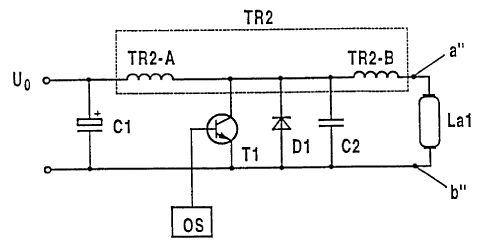
Figure 4 schematically illustrates a preferred variant
of the circuit from Figure 3, which is likewise
suitable for lamps with higher maximum pulsed voltages.
In this variant, the transformer TR1 is replaced by an
autotransformer TR2 whose primary winding TR2-A is used
as the inductive energy reservoir, and whose secondary
winding TR2-B is connected between the tuned circuit
capacitor C2 and the corresponding connection a" of the
lamp Lal. In consequence, the lamp La1 is connected by
means of the connections a",b" in parallel with the
series circuit formed by the secondary winding TR2-B
and the tuned circuit capacitor C2. One advantage of
this solution that results from this over the solution
in Figure 3 is the more favourable turns ratio. For
example, in order to triple the voltage from the lamp
supply leads in comparison with the voltage on the
primary winding TR2-A, a transformation ratio of just
two is sufficient for the autotransformer variant TR2,
owing to the electrical circuitry of the primary TR2-A
and secondary TR2-B windings, and the f act that they
are wound in the same sense. In contrast, a
transformation ratio of three is required for this
purpose in the solution from Figure 3. Apart from this,
the other function of the variant in Figure 4
corresponds to that function which has already been
described in the explanation relating to Figure 3.
Further advantages over the solution from Figure 3 are
a lower parasitic inductance and lower losses, as well
as a lower winding capacitance. Owing to the lower
winding capacitance, voltage pulses with steeper pulse
flanks are possible, which is advantageous for
efficient operation of radiators with a discharge which
is operated in a pulsed manner and is impeded
dielectrically.
CA 02267366 1999-03-19
- 13 -
Figure 5 shows measurement curves for the drive signal
for the transistor T1 (CH1) of the current through the
primary winding TR2-A (CH2) and the voltage on the lamp
Lal (CH3). The time t (one unit corresponds to 2 BLS) is
plotted on the x-axis, and the respective signal
strength is plotted, in arbitrary units, on the y-axis.
As can be seen from Figure 5, the pause time between
two voltage pulses can be influenced by the length of
the period T of the control signal. It is likewise
possible to see from Figure 5 the requirement that, on
the one hand, the duration of the switched-off time t2
of the transistor T1 must be longer than the duration t;
of the voltage pulse since, otherwise, the falling
flank of the voltage pulse is cut off. On the other
hand, the switched-off time t2 must have ended before
the zero crossing of the current through the tuned
circuit inductance L1 since, otherwise, interference
oscillations will normally occur. The pause duration
between the individual voltage pulses can be influenced
by the duration of the switched-on time tl of the
transistor Tl. The parameters switched-on time tl and.
switched-off time t2 can also be used for dimming a
connected radiation source.
Figure 6 illustrates schematically a variant of the
autotransformer circuit from Figure 4. The tuned
circuit capacitor is in this case formed by the
intrinsic capacitance of the lamp La1 (not illustrated)
or by the lamp capacitance transformed by the
autotransformer and, in addition, by the depletion
layex capacitance (not illustrated) of the MOSFET T2. A
supplementary tuned circuit capacitance in the form of
a discrete capacitor, for example as in Figure 4, is
dispensed with here. In addition, a discrete
freewheeling diode is dispensed with since its task is
carried out by the diode inherent in the MOSFET T2 (not
illustrated). The rest of the circuit and the principle
of the method of operation correspond to those in
Figure 4. The lamp Lal is in consequence connected by
CA 02267366 1999-03-19
- 14 -
means of the connections a~~, b~~ in parallel with the
series circuit formed by the secondary winding TR2-B
and the MOSFET T2. This circuit variant thus manages
with an extremely small number of components.