Note: Descriptions are shown in the official language in which they were submitted.
CA 02267492 2001-03-05
P.~TE~T
3~~~-3~-2~i
The present invention is directed to the formation of thin layer resistors,
preferably for
printed circuitry, such thin layers being capable of being embedded wi~in a
printed circuit
board. In particular, the invention is directed to forming thin layer
resistors from thin layers
of resistive material which may. be deposited by combustion chemical vapor
deposition.
Background of the Invention
Combustion chemical vapor deposition ("CCVD"), a recently invented CVD
technique, allows for open atmosphere deposition of thin films. The CCVD
process offers
several advantages over other thin-film technologies, including traditional
CVD. The key
advantage of CCVD is its ability to deposit films in the open atmosphere
without any costly
furnace, vacuum, or reaction chamber. As a result, the initial system
capitalization
requirement can be reduced up to 90% compared to a vacuum based system.
Instead of a
specialized environment, which is required by other technologies, a combustion
flame
provides the necessary environment for the deposition of elemental
constituents from
solution; vapor, or gas sources. The precursors are generally dissolved in
a~solvent that also
acts as the combustible fuel. Depositions can be performed at atmospheric
pressure and
temperature within an exhaust hood, outdoors, or within a chamber for control
of the
surrounding gases or pressure.
Because CCVD generally uses solutions, a significant advantage of this
technology is
that it allows rapid and simple changes in dopants and stoichiometries which
eases deposition
of complex films. The CCVD technique generally uses inexpensive, soluble
precursors. In
addition, precursor vapor pressures do not play a role in CCVD because the
dissolution
process provides the energy for the creation of the necessary ionic
constituents. By adjusting
solution concentrations and constituents, a wide range of stoichiometries can
be deposited
quickly and easily. Additionally, the CCVD process allows both chemical
composition and
physical structure of the deposited film to be tailored to the requirements of
the specific
application.
CA 02267492 2001-06-29
P.~TE~T
~~-l~-.i~-~.~
Unlike conventional C~'D, the CC~'D process is not confined to an expensive,
inflexible. low-pressure reaction chamber. Therefore, the deposition flame, or
bank of
flames, can be moved across the substrate to easily coat large and/or complex
surface areas.
Because the CCVD process is not limited to specialized environments, the user
can
continuously feed materials into the coating area without disruption, thereby
permitting batch
processing. Moreover, the user can limit deposition to specific areas of a
substrate by simply
controlling the dwell time of the flarne(s) on those areas. Finally, the CCVD
technology
generally uses halogen-free chemical precursors having significantly reduced
negative
environmental impact.
Numerous materials have been deposited via CCVD technology with the combustion
of a premixed precursor solution as the sole heat source. This inexpensive and
flexible film
deposition technique permits broad use of thin film technology. The CCVD
process has
much of the same flexibility as thermal spraying, yet creates quality,
conformal films like
those associated with conventional; CVD. With CCVD processing, a desired phase
can be
deposited in a few days and at relatively low cost.
A preferred embodiment of the CCVD process is described in detail in U.S.
Patent No. 5,997,596.
In accordance with that patent, a <ICVD produces vapor formed
films, powders and nanophase coatings from near-supercritical liquids and
supercritical
fluids. Preferably, a liquid or liquid-like solution fluid containing chemical
precursors) is
formed. The solution fluid is regulated to near or above the critical pressure
and is then
heated to near the supercritical temperature just prior to being released
through a restriction or
nozzle which results in a gas entrained very finely atomized or vaporized
solution fluid. The
solution fluid vapor is combusted to form a flame or is entered into a flame
or electric torch
plasmas and the precursors) react to the desired phase in the flame or plasma
or on the
substrate surface. Due to the high temperature of the plasma much of the
precursor will react
prior to the substrate surface. A substrate is positioned near or in the flame
or electric
plasma, and a coating is deposited. Alternatively, the material formed can be
collected as a
nanophase powder.
CA 02267492 1999-03-29
PATENT
3 X45-3 ~-2-1
Very tine atomization, nebulization, vaporization or gasification is achieved
using
solution fluids near or above the critical pressure and near the critical
temperature. The
dissolved chemical precursors) need not have high vapor pressure, but high
vapor pressure
precursors can work well or better than lower vapor pressure precursors. By
heating the
solution fluid just prior to or at the end of the nozzle or restriction tube
(atomizing device),
the available time for precursor chemical reaction or dissolution prior to
atomization is
minimized. This method can be used to deposit coatings from various
metalorganics and
inorganic precursors. The fluid solution solvent can be selected from any
liquid or
supercritical fluid in which the precursors) can form a solution. The liquid
or fluid solvent
by itself can consist of a mixture of different compounds.
A reduction in the supercritical temperature of the reagent containing fluid
produces
superior coatings. Many of these fluids are not stable as liquids at STP, and
must be
combined in a pressure cylinder or at a low temperature. To ease the formation
of a liquid or
fluid solution which can only exist at pressures greater than ambient, the
chemical
precursors) are optionally first dissolved in primary solvent that is stable
at ambient pressure.
This solution is placed in a pressure capable container, and then the
secondary (or main)
liquid or fluid (into which the primary solution is miscible) is added. The
main liquid or fluid
has a lower supercritical temperature, and results in a lowering of the
maximum temperature
needed for the desired degree of nebulization. By forming a high concentration
primary
solution, much of the resultant lower concentration solution is composed of
secondary and
possible additional solution compounds. Generally, the higher the ratio of a
given compound
in a given solution, the more the solution properties behave like that
compound. These
additional liquids and fluids are chosen to aid in the very fine atomization,
vaporization or
gasification of the chemical precursors) containing solution. Choosing a final
solution
mixture with low supercritical temperature additionally minimizes the
occurrence of chemical
precursors reacting inside the atomization apparatus, as well as lowering or
eliminating the
need to heat the solution at the release area. In some instances the solution
may be cooled
prior to the release area so that solubility and fluid stability are
maintained. One skilled in the
art of supercritical fluid solutions could determine various possible solution
mixtures without
undue experimentation. Optionally, a pressure vessel with a glass window, or
with optical
CA 02267492 2001-03-05
PATENT
345-3~-_'-1
fibers and a monitor, allows visual determination of miscibility and solute-
solvent
compatibility. Conversely, if in-line filters become clogged or precipitant is
found remaining
in the main container, an incompatibility under those conditions may have
occurred.
Another advantage is that release of fluids near or above their supercritical
point
results in a rapid expansion forming a high speed gas-vapor stream. High
velocity gas
streams effectively reduce the gas diffusion boundary layer in front of the
deposition surface
which, in turn, improves film quality and deposition efficiency. When the
stream velocities
are above the flame velocity, a pilot light or other ignition means must be
used to form a
steady state flame. In some instances two or more pilots may be needed to
ensure complete
combustion. With the plasma torch, no pilot lights are needed, and high
velocities can be
easily achieved by following operational conditions known by one of ordinary
skill in the art.
The solute-containing fluid need not be the fuel for the combustion.
Noncombustible
fluids like water, NZO or COZ, or diffcult to combust fluids like ammonia, can
be used to
dissolve the precursors or can serve as the secondary solution compound. These
are then
expanded into a flame or plasma torch which provides the environment for the
precursors to
react. T'he depositions can be performed above, below or at ambient pressure.
Plasma
torches work well at reduced pressures. Flames can be stable down to 10 torn,
and operate
well at high pressures. Cool flames of even less than 500 °C can be
formed at lower
pressures. While both can operate in the open atmosphere, it can be
advantageous to practice
the methods of the invention in a reaction chamber under a controlled
atmosphere to keep
airborne impurities from being entrained into the resulting coating. Many
electrical and
optical coating applications require that no such impurities be present in the
coating. These
applications normally require thin films, but thicker films for thermal
barrier, corrosion and
wear applications cari also be deposited.
Further bulk material can be grown, including single crystals, by extending
the
deposition time even further. The faster epitaxial deposition rates provided
by higher
deposition temperatures, due to higher diffusion rates, can be necessary for
the deposition of
single crystal thick films or bulk material.
CCVD is a flame process which utilizes oxygen. While it may be possible using
CCVD to deposit oxygen-reactive materials with CCVD by depositing in the
reducing
4
CA 02267492 2001-06-29
P.-~TE~T
portions of the flame, a better tech.n.ique for depositing oxygen reactive
materials, such as
nickel, is a related process described in published European Patent
Application
No. EP 0 976 847.
The invention described in published European Patent Application No. EP 0976
847
provides an apparatus and method for chemical vapor deposition wherein the
atmosphere in a
coating deposition zone is established by carefully controlling and shielding
the materials fed
to form the coating and by causing the gases removed from the deposition zone
to pass
through a barrier zone wherein they flow away from said deposition zone at an
average
velocity greater than 50 feet per minute, and preferably greater than L 00
feet per minute. The
rapid gas flow through the barrier zone essentially precludes the migration of
gases from the
ambient atmosphere to the deposition zone where they could react with the
coating or the
materials from which the coating is derived. Careful control of the materials
used to form the
coating can be provided by feeding the coating precursors in a fixed
proportion in a liquid
media. The liquid media is atomized as it is fed to a reaction zone wherein
the liquid media
is vaporized and the coating precursors react to form reacted coating
precursors.
Alternatively, the coating precursors) can be fed as a gas, either as itself
or as a mixture in a
carrier gas. The reacted coating precursors a.re often composed of partially,
fully and
fractionally reacted components, which can flow as a plasma to the deposition
zone. The
reacted coating precursors contact and deposit the coating on the surface of
the substrate in
the deposition zone. A curtain of flowing inert gases may be provided around
the reaction
zone to shield the reactive coating materials/plasma in that zone from
contamination with the
materials used in the surrounding apparatus or with components of the ambient
atmosphere.
The vaporization of the liquid media and reaction of the coating precursors in
the
reaction zone requires an input of energy. The required energy can be provided
from various
sources, such as electrical resistance heating, induction heating, microwave
heating, RF
heating, hot surface heating and/or mixing with hot inert gas.
Herein, a non-combustion process will be referred to as "Controlled Atmosphere
Combustion Cherraical Vapor Deposition" (CACCVD). This technique provides a
relatively
controlled rate of energy input, enabling high rates of coating deposition. In
some preferred
cases, the liquid media and/or a secondary gas used to atomize the liquid
media can be a
CA 02267492 1999-03-29
PATE~iT
3545-35-24
combustible fuel used in the CACCVD. Particularly important is the capability
of CACCVD
to form high quality adherent deposits at or about atmospheric pressure,
thereby avoiding the
need to be conducted in elaborate vacuum or similar isolation housings. For
these reasons, in
many cases, CACCVD thin film coatings can be applied in situ, or "in the
field", where the
substrate is located.
Combustion chemical vapor deposition (CCVD) is not suitable for those coating
applications which require an oxygen free environment. For such applications,
CACCVD,
which employs non-combustion energy sources such as hot gases, heated tubes,
radiant
energy, microwave and energized photons as with infrared or laser sources are
suitable. In
these applications it is important that all of the liquids and gases used be
oxygen-free. The
coating precursors can be fed in solution or suspension in liquids such as
ammonia or propane
which are suitable for the deposit of nitrides or carbides, respectively.
CACCVD processes and apparatus provide control over the deposition zone
atmosphere, thereby enabling the production of sensitive coatings on
temperature sensitive or
vacuum sensitive substrates, which substrates can be larger than could
otherwise be processed
by conventional vacuum chamber deposition techniques.
A further advantage of CACCVD is its ability to coat substrates without
needing
additional energy supplied to the substrate. Accordingly, this system allows
substrates to be
coated which previously could not withstand the temperatures to which
substrates were
subjected by most previous systems. For instance, nickel coatings can be
provided on
polyimide sheet substrates without causing deformation of the substrate.
Previously
atmospheric pressure deposition techniques were unable to provide chemical
vapor deposition
of metallic nickel because of its strong affinity to oxygen, while vacuum
processing of
polyimide sheet substrates was problematical due to its outgassing of water
and tendency
toward dimensional instability when subjected to heat and vacuum.
Brief Description of the Drawings
Figure 1 shows a schematic diagram of the apparatus of the invention.
Figure 2 shows a schematic diagram of an apparatus for the deposition of films
and
powders using near supercritical and supercritical atomization.
6
CA 02267492 1999-03-29
PATENT
3~~5-3~-2:~
Figure 3 shows a detailed schematic view of the atomizer used in the present
invention.
Figures 4a - -lc show in cross-sectional diagrams, steps of forming a thin
layer resistor
in accordance with the present invention; Figure 4d is a plan view of the thin
layer resistor of
Figure 4c.
Figures Sa - 5c are similar cross-sectional diagrams, illustrating steps of
forming thin
layer resistors in accordance with alternate processes of the invention.
Figure 6 is a cross-sectional view of the resistor of Figure 4c embedded in
insulating
material .
Figure 7 is a schematic view, partially in section, of an apparatus for
applying coatings
in accord with the present invention.
Figure 8 is a close-up perspective view, partially in section, of a portion of
the coating
head used in the apparatus of Figure 7.
Figures 9a-9g are cross-sectional views of structures representing a process
for
fabricating a resistor from a free-standing foil coated with an electrically
resistive material.
Figures 10 a, b and c illustrate a process of preparing a resistor pattern on
a metal foil
starting with a three-layer laminate including an electrically conductive foil
layer, an
intermediate etchable layer, and a layer of porous resistive material.
Summary of the Invention
In accordance with the present invention thin layer resistors are formed on a
substrate,
which resistors may be embedded within a printed circuit board. On a substrate
is formed a
thin layer of resistive material. Preferred resistive materials which form the
thin layers are
homogeneous mixtures of metals, such as platinum, and dielectric materials,
such as silica or
alumina. Even minor amounts of dielectric material admixed with a metal
significantly
increase the resistance of the metal. Preferably, the resistive material is
deposited on the
substrate by combustion chemical vapor deposition (CCVD). In the case of zero
valence
metals and dielectric material, the homogeneous mixture is achieved by co-
deposition of the
metal and dielectric material by CCVD. To form discrete patches of the
resistive material,
selected portions of the resistive material layer are etched away. Thus, a
layer of resistive
7
CA 02267492 1999-03-29
PATE:~iT
3~4~-3~-2-1
material may be covered with a patterned resist, e.g., an exposed and
developed photoresist,
and exposed portions of the underlying layer of resistive material etched
away. Furthermore,
the invention provides for the formation of thin layer, discrete patches of a
layer of resistive
material, and conductive material in electrical contact with spaced-apart
locations on the
patches of resistive material layer, such conductive material providing for
electrical
connection of the resistive material patches with electronic circuitry. Such
structures of
insulating material, resistive material, and conductive material may be formed
by selective
etching procedures.
Certain of the resistive materials which may be deposited by CCVD in
accordance
with the invention are porous. Such porosity facilitates etching by an etchant
which attacks
the underlying substrate. Selected portions of a porous resistive material
layer are exposed to
an etchant which seeps through the micropores in the resistive layer and
attacks the
underlying substrate material, thereby destroying adhesion between the
substrate and the
resistive material layer. Due to the thinness of the resistive material layer,
when adhesion is
destroyed, the thin layer of resistive material, in those regions exposed to
etchant, are broken
up and is carried away in the etchant, e.g., sprayed etchant. Exposure to the
etchant is limited
to a period of time sufficient to remove (ablate) the resistive material but
not long enough to
cause significant undercutting of the substrate.
In one embodiment of the invention, the resistive material layer is deposited
on a
metal foil, particularly copper foil, which foil is used to form the
conductive circuitry traces
in electrical contact with the thin layer resistors of the present invention.
Discrete patches of
resistive material are formed by use of photoimaging and ablative etching. The
resistive
material layer side of the foil is then embedded in dielectric material, e.g.,
prepreg. Then,
using photoimaging, the foil is etched into a circuitry trace pattern. This
circuitry trace
pattern is likewise embedded in dielectric material.
Because copper and/or copper oxide may interact with the resistive material
layer as it
is being deposited, in one embodiment of the invention there is deposited a
barrier layer on
the copper surface before the resistive material layer is deposited. The
barrier layer may be a
metal, such as nickel, or a layer of dielectric material, such as silica,
which is so thin that it
does not disrupt electrical contact between the copper foil and the resistive
material deposited
8
CA 02267492 2001-03-05
PATENT
3 ~-~~-3 ~-2.~
thereontop. When the resistive material layer is porous, ablative etching may
be
accomplished using an etchant which attacks the barrier layer.
Detailed Description of the Preferred Embodiments
The present invention may be understood more readily by reference to the
following
detailed description of preferred embodiments of the invention and the
Figures.
It is to be understood that the terminology used herein is for the purpose of
describing
particular embodiments only and is not intended to be limiting. It must be
noted that, as used
in the specification and the appended claims, the singular forms "a," "an" and
"the" include
plural referents unless the context clearly dictates otherwise.
The present invention provides a method for coating a substrate with a
selected
material. The method comprises, at a first selected temperature and a first
selected pressure,
dissolving into a suitable carrier to thereby form a transport solution one or
more reagents
capable of reacting (where, for a single precursor reagent, the precipitation
of the reagent
from the solution or change in chemical bonds is herein considered a
"reaction") to form the
selected material. At some time prior to~the actual deposition, a substrate is
positioned in a
region having a second selected pressure. The second selected pressure can be
ambient
pressure and is generally above 20 tort. The transport solution is then
pressurized to a third
selected pressure above the second selected pressure using a pressure
regulating means. One
of skill in the art would recognize that there are many suitable pressure
regulating means,
including, but not limited to compressors, etc. Next, the pressurized,
transport solution is
directed to a fluid conduit having an input end and an opposed output end
having a
temperature regulating means positioned thereon for regulating the temperature
of the
solution at the output end. The output end of the conduit fiuther comprises an
outlet port
oriented to direct the fluid in the conduit into the region and in the
direction of the substrate.
The outlet port can be of a shape similar to a nozzle or restrictor as used in
other spraying and
9
CA 02267492 2001-03-05
P.4TE~T
3~~1~-3~-?~
atomizing applications. Thereafter, the solution is heated using the
temperature regulating
means to a second selected temperature within ~0 °C above or below the
critical temperature,
T~, of the solution while maintaining the third selected pressure above the
second selected
pressure and above the corresponding liquidus or critical pressure, P~, of the
solution at the
second selected temperature using the pressure regulating means. Then, the
pressurized,
heated solution is directed through the outlet port of the conduit into the
region to produce a
nebulized solution spray in the direction of the substrate. As the solution is
directed into the
region, one or more selected gases are admixed into the nebulized solution
spray to form a
readable spray and, thereafter, this readable spray is exposed to an energy
source at a
selected energization point. The energy source provides sufficient energy to
react the
reactable spray (which contains the one or more reagents of the transport
solutions) thereby
forming the material and coating the substrate therewith.
In a further embodiment of this method, the energy source comprises a flame
source
and the selected energization point comprises an ignition point. In an
alternative embodiment,
the energy source comprises a plasma torch.
In a further embodiment of the method, the second selected pressure of the
region is
ambient pressure.
In yet another embodiment, the nebulized solution spray is a vapor or an
aerosol
having a maximum droplet size of less than 2 pm.
?0 In a further embodiment, the second selected pressure of the region is
reduced to
produce a combustion flame having a temperature of less than 1000 °C.
In yet another embodiment, the carrier is propane and the transport solution
comprises
at least 50 % by volume propane. In a further embodiment, the transport
solution further
includes butanol, methanol, isopropano!, toluene, or a combination thereof. In
yet another
embodiment, the carrier is selected such that the transport solution is
substantially precipitate
free at standard temperature and pressure for a period of time sufficient to
carry out the
method.
In an alternative embodiment of the method, a pressurized container is used
and before,
during or after the pressuring step, a standard temperature and pressure gas
is also contacted
CA 02267492 1999-03-29
PATEVT
3 ~:1~-3 ~-2:1
with the transport solution at a selected pressure sufficient to form a liquid
or supercritical
t~uid (depending upon the temperature). In a preferred embodiment, the
transport solution
containing the standard temperature and pressure gas is substantially
precipitate free at the
selected pressure for a period of time sufficient to carry out the method. In
yet another
embodiment, the reagent concentration of the transport solution is between
0.0005 M and
0.05 M.
In a further embodiment, the outlet end of the conduit further comprises a
fluid
introduction port and, prior to directing the pressurized, heated solution
through the outlet
port of the conduit, fluid is added to the pressurized, heated solution
through the fluid
introduction port. Such introduction forms a combined solution having a
reduced
supercritical temperature.
In yet another embodiment, each of the one or more reagents has a vapor
pressure of
no less than about 25 % of the vapor pressure of the carrier.
In a further embodiment, the outlet end of the conduit comprises tubing having
an
internal diameter of 2 to 1000 Vim, more preferably 10 to 250 Vim. In a more
preferable
embodiment, the outlet end of the conduit comprises tubing having an internal
diameter of 2~
to 125 Vim. In yet a further preferable embodiment, the outlet end of the
conduit comprises
tubing having an internal diameter of 50 to 100 Vim.
In another embodiment, the temperature regulating means comprises means for
resistively heating the conduit by applying thereto an electric current of a
selected voltage
from an electric current source. In a preferred embodiment, the voltage is
less than 115 Volts.
In yet another preferred embodiment, the means for resistively heating the
conduit comprises
a contact positioned within 4 mm of the outlet port.
Moreover, the present invention also provides the above method wherein the
carrier
and one or more reagents are selected such that the second selected
temperature is ambient
temperature.
The above method may be practiced wherein the material that coats the
substrate
comprises a metal, a metal or metalloid oxide, or a mixture of a metal with a
metal or
metalloid oxide.
11
CA 02267492 1999-03-29
P.~TE~iT
3~4~-35-?.I
In a further embodiment, the reactable spray comprises a combustible spray
having a
combustible spray velocity and wherein the combustible spray velocity is
greater than the
flame speed of the flame source at the ~.gnition point and further comprising
one or more
ignition assistance means for igniting the combustible spray. In a preferred
embodiment,
each of the one or more ignition assistance means comprises a pilot light. In
yet another
embodiment, the combustible spray velocity is greater than mach one.
In a further embodiment, the ignition point or flame front is maintained
within 2 cm.
of the outlet port.
The present invention also provides a method where, during the exposing step,
cooling the substrate using a substrate cooling means. In a preferred
embodiment, the
substrate cooling means comprises a means for directing water onto the
substrate. However.
one of ordinary skill in the art would recognize that many other suitable
cooling means could
be used.
In a further embodiment, the material that coats the substrate has a thickness
of less
than 100 nm. In yet another embodiment, the material that coats the substrate
comprises a
graded composition. In another embodiment, the material that coats the
substrate comprises
an amorphous material. In a further embodiment, the material that coats the
substrate
comprises a nitride, carbide, boride, metal or other non-oxygen containing
material.
The present invention also provides a method further comprising flowing a
selected
sheath gas around the reactable spray thereby decreasing entrained impurities
and maintaining
a favorable deposition environment.
In a preferred embodiment, the second selected pressure is above 20 torr.
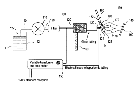
Refernng now to Figure 1, the preferred apparatus 100 comprises a pressure
regulating means 110, such as a pump, for pressurizing to a first selected
pressure a transport
solution T (also called "precursor solution") in a transport solution
reservoir 112, wherein the
transport solution T comprises a suitable carrier having dissolved therein one
or more
reagents capable of reacting to form the selected material and wherein the
means for
pressurizing 110 is capable of maintaining the first selected pressure above
the corresponding
liquidus (if the temperature is below T~) or critical pressure, P~,, of the
transport solution T at
12
CA 02267492 1999-03-29
PATE~1T
345-3j_2-1
the temperature of the transport solution T, a fluid conduit 120 having an
input end 122 in
fluid connection with the transport solution reservoir 112 and an opposed
output end 124
having an outlet port 126 oriented to direct the fluid in the conduit 120 into
a region 130 of a
second selected pressure below the first selected pressure and in the
direction of the substrate
140, wherein the outlet port 126 further comprises means 128 (see Figures 2
and 3, atomizer
4) for nebulizing a solution to form a nebulized solution spray N, a
temperature regulating
means 150 positioned in thermal connection with the output end 124 of the
fluid conduit 120
for regulating the temperature of the solution at the output end 124 within 50
°C above or
below the supercritical temperature, T~, of the solution, a gas supply means
160 for admixing
one or more gases (e.g., oxygen) (not shown) into the nebulized solution spray
N to form a
reactable spray, an energy source 170 at a selected energization point 172 for
reacting the
reactable spray whereby the energy source 170 provides sufficient energy to
react the
reactable spray in the region 130 of the second selected pressure thereby
coating the substrate
140.
I 5 In a further embodiment of the apparatus, the energy source 170 comprises
a flame
source 'and the selected energization point 172 comprises an ignition point.
In an alternate
embodiment, the energy source 170 comprises a plasma torch. In yet another
embodiment,
the outlet port 126 further comprises a pressure restriction (see Figure 3,
restrictor 7).
In a further embodiment of the apparatus, the second selected pressure of the
region is
ambient pressure.
In yet another embodiment, the nebulized solution spray N is a vapor or an
aerosol
having a maximum droplet size of less than 2 Vim.
In a further embodiment, the second selected pressure of the region is reduced
to
produce a combustion flame having a temperature of less than 1000 °C.
In yet another embodiment, the carrier is propane and the transport solution
comprises
at least 50 % by volume propane. In a further embodiment, the transport
solution further
includes butanol, methanol, isopropanol, toluene, or a combination thereof. In
yet another
embodiment, the carrier is selected such that the transport solution is
substantially precipitate
13
CA 02267492 2001-03-05
P.~TE~T
35:15-3s-'_'.i
tree at standard temperature and pressure for a period of time sufficient to
carry out the
method.
In an alternative embodiment of the apparatus, a pressurized container (not
shown) is
provided and a standard temperature and pressure gas is also contacted with
the transport
solution at a selected pressure sufficient to form a liquid or supercritical
fluid. In a preferred
embodiment, the transport solution containing the standard temperature and
pressure gas is
substantially precipitate free at the selected pressure for a period of time
suflacient to carry
out the method. In yet another embodiment, the reagent concentration of the
transport
solution is between 0.0005 M and 0.05 M.
In a further embodiment, the outlet end 124 of the conduit 120 further
comprises a
fluid introduction port (see Figure 2, feed lines 17 or 19) and, prior to
directing the
pressurized, heated solution through the outlet port 126 of the conduit 120,
fluid is added to
the pressurized, heated solution through the fluid introduction port. Such
introduction forms
a combined solution having a reduced supercritical temperature.
1 S In yet another embodiment, each of the one or more reagents has a vapor
pressure of
no less than about 25 % of the vapor pressure of the carrier.
In a further embodiment, the outlet end of the conduit comprises tubing having
an
internal diameter of 2 to 1000 Vim, more preferably 10 to 250 ~tm. In a more
preferable
embodiment, the outlet end of the conduit comprises tubing having an internal
diameter of 25
to 125 Vim. In yet a further preferable embodiment, the outlet end of the
conduit comprises
tubing having an internal diameter of SO to 100 pm.
In another embodiment, the temperature regulating means 150 comprises means
for
resistively heating the conduit by applying thereto an electric current of a
selected voltage
from an electric current source. In a preferred embodiment, the voltage is
less than 115 Volts.
In yet another preferred embodiment, the means for resistively heating the
conduit comprises
a contact 152 positioned within 4 mm of the outlet port 126.
Moreover, it is provided that the above apparatus is utilized wherein the
carrier and
one or more reagents are selected such that the second selected temperature is
ambient
temperature.
14
CA 02267492 2001-03-05
P.~TE~~T
3 ~.~~-3 ~-2-t
The above apparatus may be used wherein the material that coats the substrate
I.tO
comprises a metal. :alternatively, the material that coats the substrate 1.10
comprises one or
more metal oxides. In yet a further embodiment, the material that coats the
substrate 1.10
comprises at least 90 % silica.
In a further embodiment, the reactable spray comprises a coriybustible spray
having a
combustible spray velocity and wherein the combustible spray velocity is
greater than the
flame speed of the flame source at the ignition point 172 and further
comprising one or more
ignition assistance means 180 for igniting the combustible spray. In a
preferred embodiment.
each of the one or more ignition assistance means 180 comprises a pilot light.
In yet another
embodiment, the combustible spray velocity is greater than mach one.
In a further embodiment, the ignition point 172 or flame front is maintained
within 2
cm. of the outlet port.
The present invention also provides a substrate cooling means 190 for cooling
the
substrate 140. In a preferred embodiment, the substrate cooling means 190
comprises a
means for directing water onto the substrate 140. However, one of ordinary
skill in the art
would recognize that many other suitable cooling means could be used.
In a further embodiment, the material that coats the substrate 140 has a
thickness of
less than 100 nm. In yet another embodiment, the material that coats the
substrate 140
comprises a graded composition.
There is further provided an apparatus comprising a means (see Figures 2 and
3, feed
line 17 or 19) for flowing a selected sheath gas around the reactable spray
thereby decreasing
entrained impurities and maintaining a favorable deposition environment.
In a preferred embodiment, the second selected pressure is above 20 torr.
In a further embodiment of the method, the energy source comprises a flame
source
and the selected energization point comprises an ignition point. In an
alternate embodiment,
the energy source comprises a plasma torch, hot gasses, etc.
In a further preferred embodiment of the powder forming method, the transport
solution concentration is between 0.005 M and 5 M.
CA 02267492 1999-03-29
P:~TE~T
35~1~-35-24
To simplify the operation, it is helpful to pump the precursor/solvent
solution to the
atomizing device at room temperature. Heating of the solution should occur as
a final step
just prior to release of the solution into the lower pressure region. Such
late stage heating
minimizes reactions and immiscibilities which occur at higher temperatures.
Keeping the
solution below the supercritical temperature until atomization maintains the
dissolved
amounts of precursor in the region of normal solubility and reduces the
potential of
developing significant solvent-precursor concentration gradients in the
solution. These
solubility gradients are a result of the sensitivity of the solution strength
of a supercritical
solvent with pressure. Small pressure gradients (as they can develop along the
precursor-
solvent system delivery) can lead to significant changes in solubility as has
been observed.
For instance, the solubility of acridine in carbon dioxide at 308 °K
can be increased 1000
times by increasing the pressure from 75 atm to 85 atm. See V. Krukonis,
"Supercritical
Fluid Nucleation of Difficult to Comminute Solids", Presented at AIChE
Meeting, San
Francisco, November 25-30, 1984. Such solubility changes are potentially
detrimental
because they may cause the precursor to be driven out of solution and
precipitate or react
prematurely, clogging lines and filters.
The rapid drop in pressure and the high velocity at the nozzle cause the
solution to
expand and atomize. For solute concentrations in the normal solubility range,
preferred for
operation of the near supercritical atomization system of the present
invention, the precursors
are effectively still in solution after being injected into the low pressure
region. The term
"effectively in solution" must be understood in conjunction with processes
taking place when
a solution with solute concentrations above the normal solvent strength is
injected into the
low pressure region. In this case, the sudden pressure drop causes high
supersaturation ratios
responsible for catastrophic solute nucleation conditions. If the catastrophic
nucleation
rapidly depletes the solvent from all dissolved precursor, the proliferation
of small precursor
particles is enhanced. See D.W. Matson, J.L. Fulton, R.C. Petersen and R.D.
Smith, "Rapid
Expansion of Supercritical Fluid Solutions: Solute Formation of Powders, Thin
Films, and
Fibers", Ind. Eng. Chem. Res., 26, 2298 (1987); H. Anderson, T.T. Kodas and
D.M. Smith,
"Vapor Phase Processing of Powders: Plasma Synthesis and Aerosol
Decomposition", Am.
Ceram. Soc. Bull., 68, 996 (1989); C.J Chang and A.D Randolph, " Precipitation
of Microsize
16
CA 02267492 2001-03-05
P.~TE~T
3 ~-~ ~-3 5-2-1
Organic Particles from Supercritical Fluids". AIChE Journal, 35, 1876 ( 1989);
T.T. Kodas,
"Generation of Complex Metal Oxides by aerosol Processes: Superconducting
Ceramic
Particles and Films", Adv. Mater., 6, 180 (1989); E. Matijevic, " Fine
Particles: Science ad
Technology", MRS Bulletin, 14, 18 ( 1989); E. Matijevic, " Fine Particles Part
II: Formation
Mechanisms and Applications", MRS Bulletin, 15, 16 (1990); R.S. Mohamed, D.S.
Haverson, P.G. Debenedetti and R.K. Prud'homme, " Solid Formation After
Expansion of
Supercritical Mixtures," in Supercritical Fluid Science and Technology, edited
by K.P.
Johnston and J.M.L. Penniger, p.355, American Chemical Society, Washington, DC
(1989);
R.S. Mohamed, P.G. Debenedetti and R.K. Prud'homme, "Effects of Process
Conditions on
Crystals Obtained from Supercritical Mixtures", AIChE J., 35, 325 ( 1989); J.
W. Tom and
P.G. Debenedetti, "Formation of Bioerodible Polymeric Microspheres and
Microparticles by
Rapid Expansion of Supercritical Solutions", Biotechnol. Prog., 7, 403 ( 1991
). Particles are
undesirable for the formation of thin coatings, but can be beneficial during
the formation of
powders.
Thus the heated atomizer provides the further superior advantages, compared to
wn
unheated device that operates on rapid expansion of a solvent at exclusively
above the
supercritical temperature, that ( 1 ) the temperature allows for a well
controlled degree of
atomization of the precursor-solvent mixture and (2) catastrophic nucleation
of the precursors
can be omitted while still enjoying the benefits of supercritical atomization.
Supersonic
velocities can be created forming a mach disk which additionally benefits
atomization.
Addition of gases to the released atomized materials aids in directing the
flow and can
ensure a desired mixture for combustion.
By adjusting the heat input into the atomizing device, the liquid solution can
be
vaporized to various degrees. With no heat input to the atomizing device,
liquid solutions of
higher supercritical temperature liquids, that are liquids at STP, can exit in
the form of a
liquid stream which is clearly far from a supercritical condition. This
results in a poorly
formed flame and, possibly, undesirable liquid contact with the substrate.
Decreasing the
temperature differential of the liquid solution to its supercritical
temperature at the nozzle
causes the liquid solution to break up into droplets forming a mist which is
released from the
17
CA 02267492 2001-03-05
P.~TEV T
3 s.~~-~: -'_'~
atomizing device. The droplets vaporize, and thus become invisible, after a
short distance.
.-~s the supercritical temperature at the atomizing device is approached, the
liquid solution
droplets decrease in size, and the distance to solution vaporization is
decreased. L.'sing this
atomizer the vapor droplet size was determined using an aerosol vaporization
tester and the
obtained droplet size was below the 1.8 mm detection limit of the instrument.
Further increasing the heat input results in a state of no mist at the tip, or
complete
. vaporization. Without wishing to be bound by theory, this behavior of the
solution can be
attributed to the combined supercritical properties of the reagents and
solvents. Solutions of
precursors in lower supercritical temperature solvents, that gases at STP,
behave
similarly, but the emerging solution from the tip (also referred to as the
"nozzle" or
"restrictor") does not form a liquid stream, even without heat input. The
amount of heat
needed to obtain optimal vaporization of the solution depends mostly on the
heat capacity of
the solution and the differential between the supercritical temperature of the
solvent and the
ambient temperature around the nozzle.
It is desirable to maintain the pressure and temperature of the system (before
vaporization) above the boiling and the supercritical point of the solution.
If the pressure falls
below the liquidus or critical pressure, coincident with the temperature above
the boiling
point, vaporization of the solvents will occur in the tube prior to the tip.
This leaves the
solutes which can build up and clog the atomizing device. Similarly the
pressure is preferably
sufficiently high in the supercritical region so that the fluid is more liquid-
like. Liquid-like
supercritical fluids are better solvents than more gas-like supercritical
fluids, further reducing
the probability of solutes clogging the atomizing device. If the precursor-to-
precursor
interaction is higher than the strength between solvent and precursor; the
solvent-precursor
bonds can be broken and effectively drive the precursor out of solution.
Precursor molecules
then form clusters that adhere to the atomizing device and clog the
restrictor. The problem
can be solved, in most cases, by shifting the vaporization point from the
inside of the tip to
the end of the tip, which is accomplished by reducing the heat input into the
atomizing
device. Another solution is to use a solvent which forms stronger bonds with
the precursor so
a more stable solution is formed. A small amount of mist at the tip usually
results in the best
18
CA 02267492 2001-03-05
P.~TE~T
35-~5-35-?-1
quality thin films. Vano- or micro-spheres of the material will form if the
temperature of the
solution is too high or too low. These spheres are detrimental if dense
coatings are desired.
If the no-mist condition is reached, the deposition is being perfot~rrted
above the
critical temperature. The heat of the flame and mixing with external ~ gases
keeps STP liquid
solvents from condensing and forming droplets. In the no-mist instance,
atomization and
intermixing is very good but flow stability is reduced, resulting in a flame
that can jump from
side to side with respect to the direction of the tip. With such a flame
behavior, depositions
remain possible, but it can be difficult to deposit films requiring stringent
thickness
uniformity. Additionally, it is necessary to maintain the temperature of the
solution, prior to
release. below the temperature where either the solute precipitates or reacts
and precipitates.
When using a solvent mixture it may be possible during heating to cross the
line for spinoidal
immiscibility. This causes the formation of two separate phases, with the
possibility of
concentration differences in the two phases due to different solubilities of
the solutes. This
may influence the formation of precursor and product spheres at high
atomization
temperatures. All of these factors demonstrate the preferability of minimizing
the solution's
exposure to heating, if necessary, until the tip so that possible unwanted
equilibrium
condition states of matter do not have sufficient time to transpire. The
structure of the films
deposited can thus be precisely controlled.
Due to this control, a number of film microstructures are possible. By,
increasing
solution concentration it is possible to increase the deposition rate and the
following
microstructural changes result with increasing solution concentration; dense
to porous,
specular to dull, smooth to rough, columnar to hillocks, and thin to thick.
Graded and
multilayered coatings can also be produced. Multilayers can be formed by
supplying different
precursor containing solutions to an individual flame. Sequential multiple
deposition flames
may be used to increase throughput for production applications. Some
additional factors
controlling deposition parameters include; substrate surface temperature which
controls
surface diffusion and nucleation; pressure which controls boundary layer
thickness and thus
deposition rate, solution composition and mix gases varies the material being
deposited and
thus the coatings growth habit, flame and plasma energy level effects where
the reaction
occurs and vapor stability, and the distance to the substrate effects the time
from nebulization
19
CA 02267492 2001-03-05
P.~TE~ T
35~~-35-~.~
to reaction to deposition which can lead to particle formation or increased
diffusion time for
larger clusters. Additionally, electric and magnetic fields affect the growth
habits of some
materials, or increase deposition efficiency. One of ordinary skill in the art
would recognize
that such electric and magnetic fields will affect the growth habits of some
vapor deposited
materials, as well as vary the particular deposition rate and efficiency.
Because the required energy input into the solution heating atomizer varies
for
different precursor/primary-solvent/secondary-solvent solutions, it is
preferred to deposit
multilayer thin films from solutions with constant primary to secondary
solvent ratios. In so
doing, it is not necessary to change the energy input to the atomizer when
switching from one
solution to another solution. The resulting simplification of the setup
produces increased
performance and reliability while reducing costs. Alternatively, the substrate
can be passed
by flames containing different reagents to build the desired multilayer.
When the solution provides the fuel for combustion, concentrations up to 0.1
molar
result in dense coatings depending on the material. Most materials have
preferred
concentrations o.f up to 0.01 molar. Materials with lower diffusion and
mobility need solution
concentrations of less than 0.002. Solution concentrations of less than 0.0001
molar result in
very slow deposition rates for most materials. Flame depositions with added
combustible
materials can have higher concentrations, even exceeding 1 M, but for the
preferable vapor
formation of the precursors, high concentrations are less desirable unless the
precursors)
have high vapor pressures. Low vapor pressure precursor solution
concentrations are
preferably less than 0.002 molar.
Without wishing to be bound by theory, it is helpful to understand that the
principle of
the deposition technique of the present invention involves the finding that
CVD is not
limited to reactions at the surface. See Hunt, A.T., "Combustion Chemical
Vapor Deposition.
a Novel Thin Film Deposition Technique", Ph.D. Thesis Georgia Inst. of Tech,
Atlanta, GA.,
( 1993); Hunt, A.T., "Presubstrate Reaction CVD, and a Definition for Vapor",
presented at
the 13th Int. Conf. on CVD, ; Los Angeles, CA (1995).
Reactions can occur predominately in the gas stream, but the resulting
material which is
deposited must be subcritical in size to yield a coating with vapor deposited
~orostructures. These observations demonstrate that a vapor is composed of
CA 02267492 2001-03-05
P.aTE~T
3 515-3 ~-_'-1
individual atoms, molecules or nanoclusters which can be absorbed onto a
substrate and
readily diffused into lower energy sites or corifigurations. Thus the maximum
cluster size
must decrease with lower substrate temperatures as does the critical nucleus
size. It is known
by one of ordinary skill in the art that reagent clusters are left after
vaporization of the
solvents, and the cluster size is related to the reagent vapor pressure,
initial droplet size and
the solution concentration. Therefore, atomization of low vapor pressure
reagents, which
therefore do not gasify in the flame, must be very fine to form vapor.
Preferred liquid solvents are low cost solvents include, but are not limited
to, ethanol,
methanol, water, isopropanol and toluene. Water solutions must be fed into a
preexisting
flame, while the combustible solvents can themselves be used to form the
flame. It is
preferable, but not required, to form the bulk of the flame using the solution
rather than
feeding the solution into a flame. Lower reagent concentration results this
way, which eases
the formation of subcritical nucleus sized materials.
One preferred solvent and secondary solution fluid is propane, which is a gas
at
STP. However, it must be noted that many other solvent systems are operable.
See, e.g.,
CRC Handbook ofd ml na_-d Ph, ci c, CRC Press; Boca Raton, Florida. Propane is
preferred because of its low cost, its commercial availability, and its
safety. Many low cost
organometallics can be used in a predominately propane solution. To ease
handling, the initial
precursors can be dissolved in methana~, isopropanol, toluene or other
solvents compatible
?0 with propane. This initial solution is then placed into a container into
which liquid propane is
added. Propane is a liquid at above only about 100 psi at room temperatures.
The resulting
solution has a much lower supercritical point than the initial solution which
eases atomization
by lowering the required energy input into the atomizer. Additionally, the
primary solvent
acts to increase the polar. solubility of the propane, thus allowing higher
solution
concentrations for many reagents than would otherwise be achieved by propane
alone. As a
general rule, the polarity of the primary solvent should increase with
increasing polarity of the
solute (precursor). Isopropanol can thus aid in the solubility of a polar
solute better than
toluene. In some cases the primary solvent acts as a shield between the
secondary solvent and
a ligand on the solute. One example is the dissolution of platinum-
acetylacetonate
21
CA 02267492 2001-03-05
P.~TE~T
3 ~-~ ~-. ~-'_.~
[Pt(CH,COCHCOCH;)=J in propane, where the weight ratios between
precursor'primary
solvent and primary solvent'secondary solvent can be higher than those
required in other
systems.
Ammonia has been considered and tested as a secondary solvent for the
deposition
of coatings and powders. While ammonia is an inexpensive solvent that is
compatible with
some nitrate based precursors, it is not easily usable with other secondary
solvents and
problems stem from the general aggressiveness of pure ammonia. The atomization
properties
of ammonia were tested without the addition of a precursor and the used
pressure vessel was
significantly attacked after the experiment even when an inert Type-316
stainless steel vessel
was used. In contrast to hydrocarbon based solvents, ammonia also renders
"Bona-N"* and
"Viton"* gaskets useless after only a°few minutes. Even with a suitable
gasket material this is a
problem since the desired coatings or powders usually must not contain traces
of iron or other
elements leached from the pressure vessel wall. However, there are materials,
such as
EPDM elastomer which may be used.
Other gas-like secondary solvents that were tested and can be used include
ethane,
ethylene, ethane/ethylene mixture, propane/ethylene mixture, and
propane/ethanc mixture.
Platinum thin films were deposited from a supercritical mixture of ethane and
a platinum
metalorganic.
One useful solvent and secondary. solution fluid is propane, which is a gas at
STP. However, it must be noted that many other solvent systems are operable.
See, e.g.,
CRC Press, Boca Raton, Florida. Propane is
preferred because of its low cost, its commercial availability, and its
safety. Many low cost
organometalics can be used in a predominately propane solution. To ease
handling, the initial
precursors can be dissolved in methanol, isopropanol, toluene or other
solvents compatible
with propane. This initial solution is then placed into a container into which
liquid propane is
added. Propane is a liquid at above only about 100 psi at room temperatures.
The resulting
solution has a much lower supercritical point than the initial solution which
eases atomization
by lowering the required energy input into the atomizer. Additionally, the
primary solvent
acts to increase the polar solubility of the propane, thus allowing higher
solution
* Trademark 22
CA 02267492 1999-03-29
PATE~;T
3~~5-3~-24
concentrations for many reagents than would otherwise be achieved by propane
alone. As a
general rule. the polarity of the primary solvent should increase with
increasing polarity of the
solute (precursor). Isopropanol can thus aid in the solubility of a polar
solute better than
toluene. In some cases the primary solvent acts as a shield between the
secondary solvent and
a ligand on the solute. One example is the dissolution of platinum-
acetylacetonate
[Pt(CH3COCHCOCH3),] in propane, where the weight ratios between
precursor/primary
solvent and primary solventlsecondary solvent can be higher than those
required in other
systems.
Ammonia has been considered and tested as a secondary solvent for the
deposition
of coatings and powders. While ammonia is an inexpensive solvent that is
compatible with
some nitrate based precursors, it is not easily usable with other secondary
solvents and
problems stem from the general aggressiveness of pure ammonia. The atomization
properties
of ammonia were tested without the addition of a precursor and the used
pressure vessel was
significantly attacked after the experiment even when an inert Type-316
stainless steel vessel
was used. In contrast to hydrocarbon based solvents, ammonia also renders Buna-
N and
Viton gaskets useless after only a few minutes. Even with a suitable gasket
material this is a
problem since the desired coatings or powders usually must not contain traces
of iron or other
elements leached from the pressure vessel wall. However, there are materials,
such as
EPDM elastomer which may be used.
Other tested solvents and solvent mixtures resulted in similar quality, but
were more
complex to work with since their boiling points are significantly lower, which
required
cooling of the solution or very high pressures. The ease of handling makes
propane the
preferred solvent but the other supercritical solvents are considered
alternatives to propane in
cases where propane cannot be used, such as when a precursor that is soluble
in propane
cannot be found. Other fluids can be used to further reduce the supercritical
temperature if
desired.
One heating method is the application of an electric current between the
nozzle end,
where the precursor solution is injected into the low pressure region, and the
back of the
restriction tube. This directly heated restrictive tube method allows for fast
changes in
23
CA 02267492 1999-03-29
PATEN
3s4~-3~-24
atomization due to a short response time. The location of most intense heating
can be shifted
toward the tip by increasing the connection resistance between the tip and the
electrical lead
connected to the tip. Thin walled restriction tubes possess a larger
resistance than thick
walled tubes and decrease the response time. Other heating methods can be
applied and
several have been investigated, including but not limited to, remote resistive
heating, pilot
flame heating, inductive heating and laser heating. One of ordinary skill in
the art could
readily determine other suitable heating means for regulating the temperature
at the outlet
port of the atomizer.
Remote resistive heating uses a non-conducting restriction tube that is
located inside
an electrically heated tube. The non-conducting tube will fit tightly into the
conductive tube.
Application of an electric current to the conductive type heats that tube and
energy is
transferred into the inner, non-conductive restriction tube. This method
requires larger
heating currents compared to the directly-heated restrictive tube method and
shows longer
response times, which can be advantageous under certain conditions since the
increased
1 ~ response time results in a high degree of thermal stability. On the other
hand, pilot flame and
laser heating use the energy of the pilot flame or laser light, respectively,
to heat the
restriction tube. This can be done in a directly heated setup where the tip of
the restriction
tube is subjected to the pilot flame or laser light or in an indirectly heated
configuration where
the larger outer tube is heated. Because the amount of energy that needs to be
transferred into
the solution is quite large, the heated tube will, preferably, have a thicker
wall than in the case
of direct electrical heating or remote electrical heating. Subjecting an outer
tube to the pilot
flame or laser light allows the use of a thin walled restriction tube.
Referring now to Figures 2 and 3, an apparatus 200 for the deposition of films
and
powders using supercritical atomization is shown. The apparatus 200 consists
of a fixed or
variable speed pump 1 that pumps the reagent transport solution 2 (also called
"precursor
solution") from the solution container 3 into the atomizer (also referred to
as the "nebulizer"
or "vaporizer") 4. Figure 3 is an inset view showing a more detailed schematic
view of the
atomizer 4. The precursor solution 2 is pumped from the precursor solution
container 3
through lines 5 and filters 6 and into the atomizer 4. The precursor solution
2 is then pumped
24
CA 02267492 1999-03-29
PATEN
3 ~~5-35-2-t
into a constant or variable temperature controlled restrictor 7. Heating can
be accomplished
in many ways including, but not limited to, resistive electrical heating,
laser heating,
inductive heating, or flame heating. For resistive electrical heating, either
AC or DC current
can be used. One of the electrical connections 8 to the restrictor 7 is
preferably placed very
close to the tip of the restrictor 7. In the case of heating by a DC source,
this connection 8 or
pole can be either positive or negative. The other pole 9 can be connected at
any other point
along the restrictor 7, inside or outside the housing 10. For special
applications such as
coating the inside of tubes, where a small total atomizer size is
advantageous, it is preferable
to either connect to the restrictor 7 at the back of the housing 10 or to
connect inside the
housing 10. Gas connections at the back of the housing 10 are shown in an on-
line
arrangement but can be placed in any other arrangement that does not interfere
with the
function of the apparatus 200.
The thin gas A supply line 11, 1/16 " ID in most cases, carries a combustible
gas mix
to a small outlet 12 where it can serve as a stable pilot flame, preferably
within 2.5 cm of the
restrictor 7, for the combustion of the precursor solutions supplied via the
restrictor 7. Gas A
supply is monitored by a flow controller 13, controlling the flow of the
individual gas A mix
components, 14 and 15. The gas A fuel component 14 is mixed with the oxidizing
component 15 in a mixing "T" 16 close to or inside the atomizer 4. This late
mixing is
preferably for safety reasons because it reduces potential flash-back.
Distribution channels
inside the housing 10 connect the gas supply lines 11 to the gas A feed 17.
Gas B supply
lines 18 are used to deliver gas B from the supply 19 such that good mixing
with the
nebulized solutions spray can be accomplished. In most cases a high velocity
gas stream is
utilized. A number of gas B supply holes 20 (six for most cases, more or less
holes can be
used depending on the particular application) is placed around the restrictor
7 supplying gas B
such that the desired flow pattern is obtained. The flow properties of the gas
B stream are
influenced by such factors as gas B pressure in the gas B storage container
21, flow rate as
determined by the flow controller 13, line diameters 5, and number of supply
holes 20.
Alternatively, gas B can be fed through a larger tube coaxial to and
surrounding the restrictor
7. Once the precursor solution 2 has been pumped into the precursor supply 22
its
CA 02267492 1999-03-29
PATENT
3545-35-24
temperature is controlled by the current flow (in the case of electrical
heating) through the
restrictor 7 as determined by the power supply 23. This heating current can
then be adjusted
such that the proper amount of atomization (nebulization, vaporization) can
occur. The stable
pilot flame is then capable of igniting the nebulized reactive spray and
depositing a powder or
film on a substrate 24.
Many different coatings have been deposited using the methods and apparatuses
described herein. While propane was used in most cases as the super critical
secondary
solvent (i.e. a small amount of high precursor concentration primary solvent
was mixed with
a large amount of secondary solvent), others solvents have been used. Other
possible
secondary solvents include, but are not limited to N20, ethylene, ethane, and
ammonia.
One of ordinary skill in the art would recognize that almost any substrate can
be
coated by the method and apparatus of the present invention. A substrate can
be coated if it
can withstand the temperature and conditions of the resulting hot gases
produced during the
process. Substrates can be cooled using a means for cooling (described
elsewhere herein),
such as a water jet, but at low substrate surface temperatures, dense or
crystalline coatings of
many materials are not possible because of the associated low diffusion rates.
In addition,
substrate stability in the hot gases can be further accounted for by using a
low temperature,
low pressure flame, either with or without additional substrate cooling.
A variety of chemical precursors have been suggested for CCVD deposition of
films
and powders, and additional chemical precursors are suggested herein. In
addition to
providing the metal or metalloid element, it is required of any chemical
precursor for
CCVD that it be soluble in a suitable carrier solvent, most desirably soluble
in propane.
Furthermore, if the precursor solution is to contain precursors of more than
one metal
and/or metalloid, the chemical precursors must be mutually soluble in a
suitable carrier
solvent and chemically compatible with each other. If a precursor is not
highly soluble in a
primary solvent, such as propane, it may be initially dissolved in a secondary
solvent, such
as toluene, and subsequently introduced into the primary solvent as a solution
in the
secondary solvent, providing that the chemical precursor does not precipitate
when such a
26
CA 02267492 1999-03-29
PATEN
3~~~-3~-2:~
solution is introduced into the primary solvent. Furthermore, cost
considerations enter into
the choice of chemical precursor.
If a mixture of chemical precursors are to be provided for depositing a layer
or
powder of a particular composition, it is desirable that such precursors be
combinable as a
homogeneous "pre-solution" without the addition of any additional solvent. If
not, it is
desirable that all chemical precursors be mutually soluble in a common
solvent, the less
solvent the better, as a "pre-solution". These desired properties, of course,
facilitate
shipping and handling, particularly when the intended primary solvent is
propane or
another material which is gaseous at room temperature. Though desirable to be
able to
provide a "pre-solution", it is considered acceptable that the chemical
precursors be
mutually soluble in a deposition solution of one or more solvents and either
be prepared and
sold as such a solution or prepared on-site as a deposition solution.
For deposition, the total concentration of the precursor compounds in the
carrier
solvent is generally between about 0.001 and about 2.5 wt%, preferably between
about
0. OS and about 1.0 wt % .
For most CCVD depositions, it is preferred that the precursors be dissolved in
an
organic solvent. However, for the electrically resistive materials to which
the present
invention is directed, it is undesirable that carbon co-deposits with the
resistive material.
Some materials, nickel, for example, have a high affinity for carbon.
Accordingly,
precursors for such materials may be preferably dissolved in an aqueous and/or
ammonia
solution, in which case, the aqueous and/or ammonia and/or Nz0 solution would
be
aspirated into a hydrogen/oxygen flame for CCVD.
One of the advantages of CCVD, as performed with preferred atomizing
apparatus,
relative to other deposition methods, is that the a precursor solution
containing one or more
dissolved chemical precursors is atomized as a near-super critical liquid or,
in some cases,
as a super critical fluid. Accordingly, the amount of precursor or precursors
being burned
and deposited on a substrate or deposited in powder form is independent of the
relative
vapor pressures of the individual chemical precursors and the carrier solvent
or solvents.
This is in contrast to conventional CVD processes where individual supply
lines must be
27
CA 02267492 1999-03-29
PATENT
35:I~-3~-2.1
provided for each chemical precursor that is to be vaporized, generally within
a carrier gas,
for supply to a CVD furnace. Also, some conventional CVD precursors
disproportionate,
making it difficult to supply such a chemical precursor uniformly--another
problem readily
addressed by CCVD technology.
A Controlled Atmosphere Combustion Chemical Vapor Deposition (CACCVD)
apparatus is illustrated in Figures 7 and 8. A coating precursor 710 is mixed
with a liquid
media 712 in a forming zone 714, comprising a mixing or holding tank 716. The
precursor
710 and liquid media 712 are formed into a flowing stream which is pressurized
by pump
718, filtered by filter 720 and fed through conduit 722 to an atomization zone
724, from
which it flows successively through reaction zone 726, deposition zone 728 and
barrier zone
730. It is not required that a true solution be formed from mixing the coating
precursor 710
with the liquid media 712, provided the coating precursor is sufficiently
finely divided in the
liquid media. However, the formation of a solution is preferred, since,
generally, such
produces a more homogeneous coating.
The flowing stream is atomized as it passes into the atomization zone 724.
Atomization can be accomplished by recognized techniques for atomizing a
flowing liquid
stream. In the illustrated apparatus, atomization is effected by discharging a
high velocity
atomizing gas stream surrounding and directly adjacent the flowing stream as
it discharges
from conduit 722. The atomizing gas stream is provided from a gas cylinder or
other source
of high pressure gas. In the illustrated embodiment, high pressure hydrogen
(H,) is used both
as an atomizing gas and as a fuel. The atomizing gas is fed from hydrogen gas
cylinder 732,
through regulating valve 734, flowmeter 736 and into conduit 738. Conduit 738
extends
concentrically with conduit 722 to the atomization zone where both conduits
end allowing the
high-velocity hydrogen atomizing gas to contact the flowing liquid stream
thereby causing it
to atomize into a stream of fine particles suspended in the surrounding
gas/vapors. This
stream flows into the reaction zone 726 wherein the liquid media vaporizes and
the coating
precursor reacts to form a reacted coating precursor, which often involves
dissociation of the
coating precursor into ions of its components and results in a flowing stream
of ionic
28
CA 02267492 2001-03-05
P.~TE~'T
3 5.X5-3 5-2.~
particlzs. or plasma. The flowing stream,%plasma, passes to the deposition
zone 7'?8 wherein
the reacted coating precursor contacts the substrate 740 depositing the
coating thereon.
The flowing stream may be atomized by injecting the atomizing gas stream
directly at
the stream of liquid media/coating precursor as it exits conduit 722.
Alternatively,
atomization can be accomplished by directing ultrasonic or similar energy at
the liquid stream
as it exits conduit 722.
The vaporization of the liquid media and reaction of the coating precursor
require
substantial energy input to the flowing stream before it leaves the reaction
zone. This energy
input can occur as it passes through the conduit 722, or in the atomization
andlor reaction
zones. The energy input can be accomplished by a variety of known heating
techniques, such
as electrical resistance heating, microwave or RF heating, electrical
induction heating, radiant
heating, mixing the flowing stream with a remotely heated liquid or gas,
photonic heating
such as with a laser, etc. In the illustrated preferred embodiment, the energy
input is
accomplished by the combustion of a fuel and an oxidizer in direct contact
with the flowing
1 S stream as it passes through the reaction zone. This relatively new
technique, referred to as
Combustion Chemical Vapor Deposition (CCVD), is more fully described in
U.S. Patent No. 5,652,021. In the illustrated embodiment, the fuel, hydrogen,
is fed from
hydrogen gas cylinder 732, through a regulating valve, flowmeter 742 and into
conduit 744.
The oxidizer, oxygen, is fed from oxygen gas cylinder 746, through regulating
valve 748 and
flowmeter 750 to conduit 752. Condor: 752 extends about and concentric with
conduit 744,
which extends with and concentrically about conduits 722 and 738. Upon exiting
their
respective conduits, the hydrogen and oxygen combust creating combustion
products which
mix with the atomized liquid media and coating precursor in the reaction zone
726, thereby
heating and causing vaporization of the liquid media and reaction of the
coating precursor.
A curtain of a flowing inert gas provided around at least the initial portion
of the
reaction zone isolates the reactive gases from the materials present in the
apparatus located in
proximity to the reaction zone. An inert gas, such as argon, is fed from inert
gas cylinder 754,
through regulating valve 756 and flowmeter 758 to conduit 760. Conduit 760
extends about
and concentric with conduit 752. Conduit 760 extends beyond the end of the
other conduits
722, 738, 744 and 752, extending close to the substrate whereby it functions
with the
29
CA 02267492 1999-03-29
PATENT
354-3~-24
substrate 740 to define a deposition zone 728 where coating 762 is deposited
on the substrate
generally in the shape of the cross-section of conduit 760. As the inert gas
flows past the end
of oxygen conduit 752, it initially forms a flowing curtain which extends
about the reaction
zone, shielding the reactive components therein from conduit 760. As it
progresses down the
conduit 760, the inert gas mixes with the gases/plasma from the reaction zone
and becomes
part of the flowing stream directed to the deposition zone 728.
An ignition source is needed to initially ignite the hydrogen and oxygen. A
separate
manually manipulated lighting or ignition device is sufficient for many
applications, however
the use of such may require a temporary reduction in the flow of inert gas
until a stable flame
front is established. In some applications, the total flow of gas may be too
great to establish
an unassisted stable flame front. In such case, it is necessary to provide an
ignition device
capable of continuously or semi-continuously igniting the combustible gases as
they enter the
reaction zone. A pilot flame or a spark producing device are exemplary
ignition sources
which may be employed.
In the deposition zone 728, the reacted coating precursor deposits coating 762
on the
substrate 740. The remainder of the flowing stream flows from the deposition
zone through a
barrier zone 730 to discharge into the surrounding, or ambient, atmosphere.
The barrier zone
730 functions to prevent contamination of the deposition zone by components of
the ambient
atmosphere. The high velocity of the flowing stream as it passes through the
barner zone 730
is a characteristic feature of this zone. By requiring that the flowing stream
achieve a velocity
of at least fifty feet per minute as it passes through the barrier zone, the
possibility of
contamination of the deposition zone by components of the ambient atmosphere
is
substantially eliminated in most coating applications. By requiring that the
flowing stream
achieve a velocity of at least one hundred feet per minute the possibility of
ambient
atmosphere contamination of the deposition zone is essentially eliminated in
those coating
operations which are more highly contamination sensitive, such as the
production of TiN or
WC.
In the embodiment of Figure 7, a collar 764 is attached to and extends
perpendicularly
outward from the end of conduit 760 adjacent deposition zone 728. The barner
zone 730 is
defined between the collar 764 and the substrate 740. The collar is shaped to
provide a
CA 02267492 1999-03-29
PATENT
3~4~-3~-24
conforming surface 766 deployed close to the surface of the substrate whereby
a relatively
small clearance is provided for the exhaust of gases passing from the
deposition zone to the
ambient atmosphere. The clearance established between the conforming surface
764 of the
collar and the substrate is sufficiently small that the exhaust gases are
required to achieve the
velocity required in the barner zone for at least a portion of their passage
between the collar
and the substrate. To this end, the conforming surface 764 of the collar 762
is shaped to lie
essentially parallel to the surface of the substrate 740. When the surface of
the substrate 740
is essentially planar, as it is in the illustrated embodiment, the conforming
surface of the
substrate is also substantially planar.
Edge effects, such as elevated temperatures and residual reactive components,
which
occur adjacent the end of the conduit 760 can extend the deposition zone
beyond the area of
the substrate directly in front of the end of conduit 760. The collar 764
should extend
outward from its joinder to the conduit 760 a sufficient distance to preclude
the back-mixing
of ambient gases into the deposition zone due to a possible Venturi effect,
and to assure that
the entire area of the deposition zone, as it is extended by the previously
noted edge effects, is
protected from the backflow of ambient gases by the high velocity exhaust
gases sweeping
through the area between the collar and the substrate. The extended collar
assures that
contamination is prevented throughout the extended deposition zone. The
diameter of the
collar should be at least twice the internal diameter of conduit 760, and
preferably, should be
at least five times the internal diameter of conduit 760. The internal
diameter of conduit 760
typically is in the range of 10 to 30 millimeters, and preferably is between
12 and 20
millimeters.
In operation, the collar 764 is located substantially parallel to the surface
of the
substrate 740 being coated and at a distance therefrom of 1 centimeter or
less. Preferably, the
facing surfaces of the collar and the substrate are between 2 and 5
millimeters apart. Spacing
devices, such as three fixed or adjustable pins (not shown), may be provided
on the collar to
assist in maintaining the proper distance between the collar and the
substrate.
The embodiment illustrated in Figure 7 is particularly advantageous for
applying
coatings to substrates which are too large, or for which it is not convenient,
to be treated in a
specially controlled environment such as a vacuum chamber or a clean room. The
illustrated
31
CA 02267492 1999-03-29
P:~TEVT
33~1~-3~-24
coating technique is advantageous because it can be accomplished under
atmospheric
pressure conditions and at more convenient "in the field" locations. The
series of concentric
conduits 722, 7:8. 744, 7~2 and 760 form a coating head 768 which can be
supplied by
relatively small flexible tubes and can be sufficiently small to be portable.
Large substrates
can be coated either by having the coating head traverse the substrate
repeatedly in a raster or
similar pattern, or by traversing the substrate with an array of coating heads
arranged to
cumulatively provide a uniform coating, or by rastering an array of coating
heads. In addition
to permitting the thin film coating of articles which previously were too
large to be coated,
this technique permits the coating of larger units of those substrates which
previously were
coated under vacuum conditions. Manufacturing economies can be achieved by
coating
larger units of these substrates, especially when mass production of the
substrates is involved.
The embodiment illustrated in FIGS. 7 and 8 is also particularly suitable for
the
production of coatings which are oxidation sensitive, such as most metal
coatings. To
provide such coatings the fuel is fed through conduit 744 in proximity to the
atomized liquid
media and coating precursor, while the oxidizer is fed through conduit 752.
The atomizing
gas fed through conduit 738 and/or the liquid media fed through conduit 722
can be materials
having fuel value, they can be materials which react with the coating
precursor or they can be
inert materials. When the produced coatings or coating precursor materials are
oxygen
sensitive, a reducing atmosphere is maintained in the reaction and deposition
zones by
assuring that the total amount of oxidizer fed is restricted to an amount less
than that required
to fully combust the fuel provided to the reaction zone, i.e. the oxidizer is
provided in less
than stoichiometric amount. Generally, the fuel excess is limited so as to
limit any flame
zone which develops when the residual hot gases mix with atmospheric oxygen.
When the
produced coatings and the precursor materials are oxygen-tolerant or enhanced
by the
presence of oxygen, such as in the production of most of the oxide coatings,
an oxidizing or
neutral atmosphere may be provided in the reaction and deposition zones by
feeding a
stoichiometric or excess amount of oxidizer. Further, with oxygen tolerant
reagents and
products, the oxidizer can be fed through the inner conduit 744 while fuel is
fed through outer
conduit 752.
32
CA 02267492 2001-03-05
P.-~TE~T
35.5-35-2-1
The inert gas supplied through conduit 760 must be sufficient to shield the
inside
surface of the conduit tiom the reactive gases produced in the reaction zone.
and it must be
sufficient, when added with the other gases from the reaction zone, to.~rovide
the gas velocity
required in the barrier zone.
The energy input can be accomplished by mechanisms other than the combustion
method illustrated in FIGS. 7 and 8. For instance, it could be accomplished by
passing
electrical current through conduit 722 to create electrical resistance heat in
the conduit ~.vhich
then transfers to the liquid medium and coating precursor as it passes through
the conduit. It
should be apparent that all of the conduits 722, 738, 744, 752 and 760 are not
required when
the energy input is accomplished by other than the combustion method. Usually
one or both
of conduits 744 and 752 are omitted when the energy input is provided by one
of the
electrically derived energy input mechanisms.
The porosity or density of the deposited coating can be modified by varying
the
distance between the flame zone and the deposition zone at the substrate's
surface. Generally,
shortening of this distance provides an increased coating density, while
increasing the
distance provides a more porous coating.
In the illustrated CACCVD technique the reaction zone is generally coextensive
with
the flame produced by the burning fuel. Of course, the flame zone and the
substrate must be
maintained sufficiently far apart that the substrate is not damaged by the
higher;temperatures
which would result as the flame zone more closely approaches the substrate
surface. While
substrate temperature sensitivity varies from one substrate material to the
next, the
temperature in the deposition zone at the substrate surface, typically, is at
least 600°C cooler
than the maximum flame temperature.
When some of the alternative methods are used to supply the energy input, such
as when
the principal energy input is a preheated fluid which is mixed with the
flowing stream in, or
before it reaches, the reaction zone, the maximum temperatures produced in the
reaction zone
are substantially lower than those produced with a combustion energy input. In
such cases
the coating properties can be adjusted by varying the distance between the
reaction zone and
at the substrate surface with less concern for overheating the substrate.
Accordingly, the
terms reaction zone and deposition zone are useful in defining functional
regions of the
33
CA 02267492 2001-03-05
P.~TE~ T
3 ~~5-3 ~-2-~
apparatus but are not intended to define mutually exclusive regions, i.e. in
some applications
reaction of the coating precursor may occur in the deposition zone at the
substrate surface.
The lower maximum temperatures resulting when the principal energy input is
other
than a combustion flame enables the use of temperature sensitive coating
materials, such as
some organic materials. In particular, polymers may be deposited as protective
coatings or as
dielectric interlayer materials in capacitors, integrated circuits or
microprocessors. For
instance, a polyimide coating could be provided from its polyamic acid
precursor. Similarly,
polytetrafloroethylene coatings could be provided from low molecular weight
precursors.
The energy input to the flowing stream prior to its leaving the reaction zone
generally
negates the need to provide energy to the deposition zone by heating the
substrate, as is often
required in other coating techniques. In the present deposition system, since
the substrate acts
as a heat sink to cool the gases present in the deposition zone, rather than
heating them, the
temperatures to which the substrates are subjected are substantially less than
are encountered
in systems which require that energy be transmitted to the deposition zone
through the
substrate. Accordingly, the CACCVD :oating process can be applied to many
temperature
sensitive substrate materials which can not be coated by techniques which
involve heating
through the substrate.
A wide range of precursors can be used as gas, vapor or solutions. It is
preferred to
use the lowest cost precursor which yields the desired morphology. Suitable
chemical
precursors, not meant to be limiting, for depositing various metals or
metalloids are as
follows:
Pt platinum-acetylacetonate [Pt(CH3COCHCOCH3)ZJ (in toluene/methanol),
platinum-(HFACZ), diphenyl-(1,5-cyclooctadiene) Platinum (II) [Pt(COD) in
toluene-
propane]
platinum nitrate (in aqueous ammonium hydroxide solution)
Mg Magnesium naphthenate, magnesium 2-ethylhexanoate [Ma(OOCCH(C,Hs)C,H9),_],
magnesium naphthenate, Mg-TMHD, Mg-acac, Mg-nitrate, Mg-2,4-pentadionate
Si tetraethoxysilane [Si(OCzHs),J, tetramethylsilane, disilicic acid,
metasilicic acid
P triethyl phosphate [CZH30)3PO,J, triethylphosphite, triphenyl phosphite
La lanthanum 2-ethylhexanoate [La(OOCCH(CZHs)C,Fi9)~] lanthanum nitrate
[La(N03)3], La-acac, La-isopropoxide,
tris (2,2,6,6-tetramethyl-3,5- heptanedionato), lanthanum [La(C"H,90,)3]
34
CA 02267492 2001-03-05
PATEVT
3 ~4~-3~-?~
Cr chromium nitrate [Cr('~10,),), chromium 2-ethylhexanoate
[Cr(OOCCH(C.HS)C,H9),), Cr-sulfate,
chromium carbonyl, chromium(III) acetylacetonate
Ni nickel nitrate [:~li(NOs),) (in aqueous ammonium hydroxide);
Ni-acetylacetonate, Ni-
2-ethylhexanoate, Ni-naphthenol, Ni-dicarbonyl
A1 aluminum nitrate [Al(NO,)3], aluminum acetylacetonate
[AI(CH,COCHCOCH,),],
triethyl aluminum, Al-s-butoxide, Al-i-propoxide, Al-2-ethylhexanoate
Pb Lead 2-ethylhexanoate [Pb(OOCCH(CzHs)C,Hq)z], lead naphthenate,
Pb-TMHD,
Pb-nitrate
. Zr zirconium 2-ethylhexanoate [Zr(OOCCH(CZHs)C,H9),J, zirconium
n-butoxide,
zirconium (HFACz), Zr-acetylacetonate, Zr-n-propanol, Zr-nitrate
Ba barium 2-ethylhexanoate [Ba(OOCCH(C2H3)C,Hg)zJ, Ba-nitrate,
Ba-acetylacetonate, Ba-TMHD
Nb niobium ethoxide, tetrakis(2,2,6,6-tetramethyl-3,5-heptanedionato)
niobium
Ti titanium (IV) i-propoxide [Ti(OCH(CH3)z),], titanium (IV)
acetylacetonate,
titanium-di-i-propoxide-bis-acetylacetonate, Ti-n-butoxide,
Ti-2-ethylhexanoate, Ti-oxide bis(acetylacetonate)
Y yttrium 2-ethylhexanoate [Y(OOCCH(C2Hs)C,Hq)3J, Y-nitrate,
Y-i-propoxide,
Y-naphthenoate
Sr strontium nitrate [Sr(N03)z], strontium 2-ethylhexanoate,
Sr(TMHD)
Co cobalt naphthenate, Co-carbonyl, Co-nitrate,
Au chlorotriethylphosphine gold (I), chlorotriphenylphosphine
gold(I)~
B trimethylborate, B-trimethoxyboroxine
K potassium ethoxide, potassium t-butoxide,
potassium 2,2,6,6-tetramethylheptane-3,5-dionate
Na sodium 2,2,6,6-tetramethylheptane-3,5-dionate, sodium ethoxide,
sodium t-butoxide
Li lithium 2,2,6,6-tetramethylheptane-3,5-dionate,
lithium ethoxide lithium-t-butoxide
Cu Cu(2-ethylhexonate)~, Cu-nitrate, Cu-acetylacetonate
Pd palladium nitrate (in aqueous ammonium hydroxide solution)
(NH,)zPd(NOz)z,
Pd-acetylacetonate, ammonium hexachloropalladium
Ir HZIrCib (in 50~ ethanol in water solution), Ir-acetylacetonate,
Ir-carbonyl
Ag silver nitrate (in water), silver nitrate, silver fluoroacetic
acid, silver acetate
Ag-cyclohexaneburyrate, Ag-2-ethylhexanoate
Cd cadmium nitrate (in water), Cd-2-ethylhexanoate
Nb niobium (2-ethylhexanoate)
Mo (NH,)6Mo,Oz,, Mo(CO)6, Mo-dioxide bis (acetylacetonate)
Fe Fe(N03)3~9HZ0, Fe-acetylacetonate
Sn SnC12~2H20, Sn-2-ethylhexanoate, Sn-tetra-n-butyltin, Sn-tetramethyl
In In(N03)yxHzO, In-acetylacetonate
Bi Bismuth nitrate, Bismuth 2-ethyl hexanoate
Ru Ru-acetylacetonate
Zn Zn-2-ethyl hexanoate, Zn nitrate, Zn acetate
CA 02267492 1999-03-29
PATENT
345-3~-2:I
W W-hexacarbonyl. W-hexafluoride, tungstic acid
In most cases where a mixture of metal precursors and/or metalloid precursors
are
deposited, the deposition is generally stoichiometric with respect to the
relative proportions
of the metals) and/or metalloids) provided by the precursors in the reaction
mixtures.
However, this relationship is neither precise nor entirely predictable.
Nevertheless, this
does not present any significant problem in achieving a coating layer or
powder of desired
composition because the relative amounts of chemical precursors required to
obtain a
coating layer or powder of desired composition can be readily determined
without undue
experimentation for any set of coating parameters. Once a ratio of chemical
precursors
under a set of coating parameters is determined to obtain a coating or powder
of desired
composition, the coating can be duplicated with highly predictable results.
Thus, if one
desired a coating or powder that would contain two metals in a particular
predetermined
ratio, one might start out with two chemical precursors containing the two
metals in the
predetermined stoichiometric ratio. If determined that the two metals were not
deposited in
the predetermined ratio, adjustments would be made in the relative amounts of
the two
precursor chemicals until the desired ratio of metals in the deposited
materials was
achieved. This empirical determination would then be relied upon for future
depositions.
CCVD has the advantages of being able to deposit very thin, uniform layers
which
may serve as the dielectric layers of embedded capacitors and resistors. For
embedded
resistors, the deposited layers are typically at least about 40 ~ thick. The
material can be
deposited to any desired thickness; however, for forming resistive material
layers by
CCVD, thicknesses seldom exceed 50,000 ~ (5 microns). Generally film
thicknesses are in
the 100-10,000 /~ range, most generally in the 300-5000 l~ range. Because the
thinner the
layer, the higher the resistance and the less material, e.g., platinum used,
the ability to
deposit very thin films is an advantageous feature of the CCVD process. The
thinness of
the coating also facilitates rapid etching in processes by which discrete
resistors are formed.
Examples of coatings produced by CCVD include silicon dioxide coatings
produced
from a solution of tetraethoxysilane [Si(OCZHS)4] in isopropanol and propane;
platinum
coatings produced from a solution of platinum-acetylacetonate
[Pt(CH3COCHCOCH3),] in
36
CA 02267492 1999-03-29
PATEN
3 ~~~-3 ~-?4
toluene and methanol: and nickel-doped LaCrO; coatings produced from solutions
of
lanthanum nitrate in ethanol, chromium nitrate in ethanol and nickel nitrate
in ethanol.
The electrical resistance of a resistor is determined by the resistivity of
the material, as
well as the length and cross-sectional area of the resistor. While very thin
films are desirable
from the standpoint of material efficiency, where power loading (current flow)
is high, thicker
films may be required. For higher power loading requirements where thicker
films are
required, the resistivity of the material may need to be higher, e.g., by
using more heavily
doped metals as the resistive material.
Novel resistive materials can be deposited by CCVD and CACCVD such that very
small, discrete electrical resistors can be formed by CCVD and CACCVD
processes in
conjunction with conventional or modified printed circuit board technology.
The novel
resistive materials are formed by the co-deposition by CCVD and CACCVD of
conductive
materials, particularly metals, such as platinum and nickel, with highly
resistive (dielectric)
materials, such as silica. It is found that a very small amount of the highly
resistive
material, e.g., about 0.1 wt% to about 20 wt%, very profoundly reduces the
conductive
properties of the conducting material. For example, platinum, though an
excellent
conductor, when co-deposited with between 0.1 and about 5 wt% silica, serves
as a
resistor, the resistance being a function of the level of silica co-deposited.
While applicants
are not bound by theory, it is believed that when a conductor and a minor
amount of a non-
conductor are co-deposited by CCVD or CACCVD, the non-conductor is deposited
generally homogeneously throughout the conductor, either as single molecules
or as
nanoclusters of molecules.
For resistive material which is a mixture of a conductive metal and a minor
amount
of a dielectric material, to be deposited by CCVD or CACCVD, the metal must be
capable
of being deposited as a zero valence metal from an oxygen-containing system if
the resistive
material is to be deposited by CCVD or CACCVD. The criteria for deposition in
the zero
valence state using a flame is that the metal must have a lower oxidation
potential than the
lower of the oxidation potential of carbon dioxide or water at the deposition
temperature.
(At room temperatures, water has a lower oxidation potential; at other
temperatures carbon
37
CA 02267492 2001-03-05
P:~TE~T
3 ~.~~-3 ~-'_'-~
dioxide has a lower oxidation potential. ) Zero valence metals which can be
readily
deposited by CCVD are chose having oxidation potentials about equal to silver
or below.
Thus, Ag, Au, Pt, and Ir can be deposited by straight CCVD. Zero valence
metals having
somewhat higher oxidation potentials may be deposited by CACCVD I~which
provides a
more reducing atmosphere. Ni, Cu, In, Pd, Sn, Fe, Mo, Co and Pb are best
deposited by
CACCVD. Herein, metals also include alloys that are mixtures of such zero-
valence
metals. The preferred dielectric materials being capable of co-deposition with
the zero
valence metals are metal oxides or metalloid oxides, such as silica, alumina,
chromia,
titania, ceria, zinc oxide, zirconia, phosphorus oxide :, bismuth oxide,
oxides of rare earth
metals in general, and mixtures thereof. Silicon, aluminum, chromium,
titanium, cerium,
zinc, zirconium, magnesium, bismuth, rare earth metals, and ~ phosphorus ,
each have
relatively high oxidation potentials, such that if any of the metals mentioned
above are
codeposited with the suggested precursors for electrically resistive material,
the metals will
deposit in zero valence state and the dopant will deposit as the oxide. Thus,
even when no
flame is used the dielectric needs to have a higher oxidation, phosphidation,
carbidation,
nitrodation, or boridation potential to form the desited two phases.
Again, for more oxygen-reactive metals and alloys of metals, CACCVD may be the
process of choice. Even if the metal can be deposited as a zero valence metal
by straight
CCVD, it may be desirable to provide ~. controlled atmosphere, i.e., CACCVD,
if the
substrate material on which it is to be deposited is subject to oxidation. For
example,
copper and nickel substrates are readily oxidized, and it may be desired to
deposit onto
these substrates by CACCVD.
Another type of resistive material which can be deposited as a thin layer on a
substrate by CCVD is "conductive oxides" . In particular, BhRu20, and SrRu03
are
conductive oxides which may be deposited by CCVD. Although these materials are
"conductive", their conductivity is relatively low when deposited in amorphous
state; thus,
a thin layer of such mixed oxides can be used to form discrete resistors. Like
conductive
metals, such "conductive oxides" may be doped with dielectric materials, such
as metal or
metalloid oxides, to increase their resistivity. Such mixed oxides may be
deposited either
38
CA 02267492 1999-03-29
PATENT
354-3 ~-?.~
as amorphous layers or as crystalline layers, amorphous layers tending to
deposit at low
deposition temperatures and crystalline layers tending to deposit at higher
deposition
temperatures. For use as resistors, amorphous layers are generally preferred,
having
higher resistivity than crystalline materials. Thus, while these materials are
classified as
"conductive oxides" in their normal crystalline state, the amorphous oxides,
even in un-
doped form, may produce good resistance. In some cases it may be desired to
form low
resistance, 1-100, resistors and a conduction-enhancing dopant, such as Pt,
Au, Ag, Cu
or F, may be added. If doped with dielectric material, e.g., metal or
metalloid oxides, to
increase resistivity of the conducting oxides, or conduction-enhancing
material to decrease
resistivity of the conducting oxides, such homogeneously mixed dielectric or
conduction-
enhancing material is generally at levels between about 0.1 wt% and about 20
wt% of the
resistive material, preferably at least about 0.5 wt% .
There are a variety of other "conducting materials" which though electrically
conducting, have sufficient resistivity to form resistors in accordance with
the present
invention. Examples include yttrium barium copper oxides and Lat_xSrxCo03,
0<_x<_ 1, e.g.,
x=0.5. Generally, any mixed oxide which has superconducting properties below a
critical
temperature can serve as electrically resistive material above such critical
temperature.
Deposition of such a variety of resistive materials is possible with proper
selection of
precursors selected from those described herein above.
To produce a metal/oxide resistive material film, precursor solution is
provided
which contains both the precursor for the metal and the precursor for the
metal or metalloid
oxide. For example, to produce platinum/silica filins, the deposition solution
contains a
platinum precursor, such as platinum(II)-acetylacetonate or diphenyl-(1,5-
cyclooctadiene)
platinum (II) [Pt(COD)] and a silicon-containing precursor, such as
tetraethoxysilane. The
precursors are mixed generally according to the ratio of metal and the metal
or metalloid
(that will form the oxide) to be deposited as a film; however, exact ratios
must be determined
empirically for any desired ratio of metal to oxide. Accordingly, precursor
solutions for
forming resistive films in accordance with the invention contain a precursor
that forms the
39
CA 02267492 1999-03-29
PATEN
3s~5-3~-24
metal and a precursor that forms the oxide at a weight ratio of between of
between about
100:0.2 to about 100:20.
Similarly, when conducting oxides are deposited to form a resistive material
layer,
precursors of each metal, e.g., Bi and Ru, and Sr and Ru, are provided in
appropriate ratios so
as to provide the correct stoichiometry ~f the conducting oxides. Again, some
experimentation may be required to provide the precursors in a precise ratio
for any particular
deposition conditions so as to produce the desired stoichiometry of the mixed
oxide. Also,
where the conducting oxide is to be doped with a dielectric metal oxide or
metalloid oxide to
increase the resistivity of the material being deposited, or conduction-
enhancing material to
decrease the resistivity of the material being deposited, an additional
precursor is provided so
as to produce minor amounts of the metal oxide or metalloid oxide, e.g.,
between 0.1 and 20
wt%, preferably at least about 0.5 wt%, of the deposited doped conducting
metal oxide.
Either of the above-mentioned platinum precursors are soluble in toluene.
Dissolving
the platinum precursors is facilitated by sonification. To a solution of the
platinum
precursor, it is convenient to add tetraethyloxysilane dissolved in methanol,
isopropanol or
toluene to form a precursor solution. The precursor solution can then be
further diluted to
a desired concentration with propane or other organic solvents.
Generally, for shipping, storage, and handling, the precursor chemicals are
dissolved in common liquid organic solvents, such as toluene, isopropanol,
methanol,
xylene, and mixtures thereof, to a concentration (of total precursor
chemicals) of between
about 0.25 and about 20 wt% , preferably at least about 0.5 wt% and typically
up to about 5
wt %a . Generally, for shipping and handling it is desired to provide
concentrations in a
concentrated form to minimize cost and minimize the quantity of flammable
liquids. At the
same time, stability, particularly low temperature stability, e.g., down to -
20°C must be
consider, lest an overly concentrated solution precipitate from solution. At
the time of
deposition, the precursor solutions are typically further diluted, e.g., in
propane, to a
concentration (of total precursor chemicals) to between about 0.005 and about
1.0 wt % ,
preferably to between about 0.05 and about 1.0 wt% , more preferably no more
than about
0.6 wt%.
CA 02267492 2001-03-05
PATEVT
3545-35-'_'.~
One of the most important metals which can be deposited in doped or undo~d
form
by CACCVD is nickel. Nickel is inexpensive and can be selectively etched
relative to
conductive metals, such as copper. An important precursor for depositing zero
valence
nickel by CACCVD is nickel nitrate. Nickel may be deposited from an ammoniacal
aqueous solution of nickel nitrate. However, as described above, it is
preferred that
deposition be from a liquid at conditions approaching supercritical. To this
end,
advantageous carriers for nickel nitrate include liquefied ammonia or
liquefied nitrous oxide
(N=O). Nitrous oxide may be liquefied by pressurizing to 700-800 psi. Ammonia
may be
liquefied by pressurization and/or low temperatures. Whether the carrier is
liquefied
ammonia or liquefied nitrous oxide, it is found advantageous to add a minor
portion of
water, i.e., up to about 40 wt% , preferably between about 2 to about 20 wt% ,
(the
liquefied ammonia or liquefied nitrous oxide comprising the balance, between
about 60 and
about 100 wt% ). The water raises the supercritical point of either liquefied
ammonia or
liquefied nitrous oxide. This makes it easier to operate sufficiently below
the supercritical
point such that variations in viscosity and density are.not encountered. Also,
the addition
of water reduces the instability of the solutions. (It is to be understood,
however, that
depositions may, in some cases, be carried out in liquified ammonia or
liquefied nitrous
oxide without the addition of water.) In such nickel deposition solutions, the
nickel
precursor along with any precursor for. a nickel dopant are typically 'present
at a low level,
i.e., from about 0.001 wt% to about 2.5 wt%. Currently preferred dopants for
nickel are
nickel phosphorus and/or nickel phosphorus oxides, e.g., nickel phosphate. It
is
believed that when using a phosphorus-containing precursor, such as phosphoric
acid, the
major dopant species is nickel phosphate. Precursor solutions in which water
and either
liquefied ammonia or NZO are the carrier co-solvents are advantageous in that
no carbon is
present which could result in deposition of carbon.
When preparing a precursor solution of nickel nitrate to be carried in
liquefied
ammonia, the nickel nitrate may be conveniently pre-dissolved in ammonium
hydroxide
solution along with precursor for any dopant, and this solution then adi~nixed
with liquefied
ammonia.
41
CA 02267492 1999-03-29
PATEN
3~4~-3~-2.~
The resistive materials described herein can be fabricated into resistors,
either as
embedded resistors, or as resistors on the surface of a printed circuit board
within
integrated circuits or other electronic applications. This is generally
accomplished using a
photoresist which is used to form a resist pattern over the layer of resistive
material and
using an appropriate etchant to remove the resistive material in areas not
covered by the
resist. For metal/oxide resistive material layers, the etchant chosen is an
etchant for the
metal component of the resistive material. Typically such etchants are acids
or Lewis
acids, e.g., FeCl3 or CuCl2 for copper. Nitric acid and other inorganic acids
(e.g.,
sulfuric, hydrochloric, and phosphoric) may be used to etch nickel, a variety
of other
metals which may be deposited as well as conductive oxides.
Aqua Regia may be used for etching noble metals, such as platinum. Aqua Regia
is
an extremely corrosive acid mixture which, herein, is useful for etching
metals, particularly
noble metals, such as platinum and gold. Au can also be etched in a potassium
iodide/iodine (KI/IZ) solution. Because CCVD uses a flame, thereby tending to
produce
oxides, only the less reactive metals, i.e., those having low oxygen
potentials, are easy to
deposit as metals, rather than as oxides. Easiest to deposit are the noble
metals, such as
platinum and gold. While these metals are, of course, costly, CCVD can be
advantageous
in that it can be used to deposit very thin, but nevertheless uniform, films.
Accordingly,
deposition by CCVD of thin layers of noble metals is, in many cases practical.
Furthermore, as noble metals are non-oxidizing, their use in high quality
electronic
applications may easily be economically justified.
Also, although noble metals are conductors, it is found that in depositing
noble
metals along with relatively minor amounts of oxides, such as silica or
alumina, the
deposited material becomes highly resistive. Accordingly, metals, such as
platinum,
containing minor amounts, e.g., 0.1%-5% of an oxide, can serve as resistors in
printed
circuit board. Such material can be deposited as a layer on a printed circuit
board and then
processed by printed circuit board techniques to provide discrete resistors.
42
CA 02267492 2001-03-05
PATENT
3315-3~-2~
However, noble metals, by their non-reactive nature, are difficult to etch, as
is
required in many processes for production of printed circuit boards. Aqua
regia is an
etchant for metals, particularly noble metals, in printed circuit board.'
processes.
Aqua regia is made from two well-Irnown acids: 3 parts concentrated (12N17
hydrochloric acid (HCl) and 1 part concentrated (16M) nitric acid HNOj . Thus,
the molar
ratio of hydrochloric acid to nitric acid is 9:4, although slight variations
from this ratio,
i.e., 6:4 to 12:4 would be acceptable for etching purposes in accordance with
the invention.
Because of its corrosive nature and limited shelf life, Aqua regia is not sold
commercially,
but must be prepared on site. To reduce its corrosiveness, the Aqua regia may
be diluted
with water up to about a 3:1 ratio of water to aqua regia. Dilution with
water, of course,
increases the etching time, but good etching times of platinum are achievable
with a 33 %
aqua regia solution. Of course, more reactive metals, such as copper, will be
easily etched
as well by aqua regia. On the other hand, the noble metals, such as platinum,
are not
etched by many of the materials suitable for etching copper, such as FeC~ or
CuClz,
thereby allowing for a variety of selective etching options in forming printed
circuit boards.
The speed of etching will depend upon several factors including the strength
of the
aqua regia and the temperature. Preferably the aqua regia is prepared fresh.
Typically,
aqua regia etching is conducted in the 55 - 60°C range, although this
may be varied depending
upon the application.
The following discussion of formation of discrete resistors assumes the use of
a
platinum-based resistive material because platinum/silica is the currently
preferred CCVD-
deposited resistive material. However, it is to be understood that the other
resistive
materials, including both metal/oxide and conducting oxide films as described
above, can
be substituted. Likewise, in techniques described hereinafter in which copper
and
platinum-based resistive layers are selectively etched, it is to be umierstood
that there are
selective etchants available for a variety of conductor/resistive material
combinations in
accordance with the invention.
In its simplest form, a resistor 400 in accordance with the invention is
merely a
patch or strip 401 (FIGs. 4c and 4d) of the thin layer resist material on an
insulating
43
CA 02267492 2001-03-05
P.~TE~T
3~4~-3~-2.~
substrate 402 with means, such as a contacting copper patch 403 at each ends
to provide for
electrical connection of the resistor to electronic circuitry. The substrate
402 might be a
flexible sheet, such as a polyimide sheet, a rigid epoxy/fiberglass board, or
even liquid
crystal sheet material. Suitable substrates desired for many applications are
films of
organic polymers, such as polyimide, having thicknesses of about 10 microns or
less.
After optimizing deposition parameters, it was found, herein, that CCVD can
apply
resistive material layers to insulating substrates, such as polyimide, without
burning or
deforming the substrates. Direct deposition of the resistive material layer on
an insulating
substrate generally provides good adhesion of the resistive material layer to
the insulating
substrate. Usually, such adhesion is better than prior art techniques which
use an adhesive
to bind a resistive material to a substrate. To form a discrete resistor 400,
a thin layer of
resist material 401(4x) is deposited by CCVD on an insulating substrate 402 to
form the
structure of FIG 4a. A chemical-resistant photoresist, such as that sold by
Morton
Electronic Materials as "Laminar 5038"* which is resistive to aqua regia (in
the case of
platinum etching), is applied to the exposed surface of the resist material
and patterned by
conventional photoimaging techniques. Generally, a resist which will withstand
very
highly acidic conditions, such as gold-plating conditions, will be suitable as
a resist for
etching with aqua regia. The exposed portions of the resist material layer are
then etched
away, by aqua regia in the case of noble metal-based resist materials, leaving
the patches or
strips 401(4b) of resist material so as to form the structure of FIG. 4b.
Copper connecting
patches 403 may then be appliai to the ends of the strips 401 to form the
resistor 400 of
FIG. 4c.
Preferably, however, in reference to FIGS. 5a - Sc, both the thin layer resist
material patches 401 and the electrical connection conductive patches 403 are
formed by
photoimaging techniques. Shown in FIG. 5a is a three-layer structure 409 which
comprises
an insulating substrate 402, a layer of resist material 401(5x), e.g.,
Pt/silica, formed in
accordance with the invention by CCVD and a conductive layer 403(5x), e.g.,
copper,
formed by CCVD or another technique, such as electrolytic plating.
* Trademark
44
CA 02267492 1999-03-29
PATENT
3~4~-3~-24
The structure 409 of FIG. 5a might be patterned in one of two two-step
procedures
by photoimaging technology. In one procedure (with reference to FIG. 5b), the
conductive
material layer 403(5a) would be covered with a resist, the resist patterned by
photoimaging
techniques, and, in the exposed areas of the resist, both the conductive
material layer and
the underlying resistive material layer be etched away, e.g., with aqua regia
to give the
structure of FIG. 5b having a patterned resistive material patch (401(5b)) and
a patterned
conductive material patch (403(5b)). Next, a second resist would be applied,
photoimaged,
and developed. This time, only the exposed portions of the conductive material
patch
403(5b) would be etched away by etchant which would selectively etch the
conductive
layer, but not the resistive material patch, i.e., FeCl3 or CuClz in the case
of Cu as the
conductive material layer and Pt/silica as the electrically resistive
material, thereby
producing the resistor structure 400 of FIG. 4c. In an alternate procedure
(with reference
to FIG.Sc), a patterned resist layer would be formed, exposed portions of the
conductive
material layer 403(5a) etched away, e.g., with FeCl3, a further patterned
resist layer
formed, and then the exposed areas of the resistive material layer (401(5b))
etched away
with aqua regia so as to form the electrical contacts 403 and give the
resistor structure 400
of FIG. 4c. By either procedure, discrete thin layer resistors 400 are formed
by
conventional photoimaging techniques common to printed circuitry formation.
Still another way of forming discrete resistors is to start with a two-layer
structure
such as that shown in FIG. 4a having a layer of resistive material, e.g.,
Pt/silica, on an
insulating substrate. Using a photoresist process, discrete patches or strips
of the resistive
material are formed on the substrate, giving a structure such as that shown in
FIG. 4b.
Next, a layer of conductive material, e.g., copper, is formed on the resistive
patches or
strips, e.g., by electrolytic plating, giving a structure such as is shown in
FIG. 5b. A
further photoresist is applied and imaged, and exposed portions of the
conductive material
are then etched away so as to leave the conductive electrical connection
patches 403 and
provide a resistor structure 400 such as is shown in FIG. 4c.
While the resistor 400 of FIG 4c could be at the surface of a printed circuit
board
device, the resistors will, in most cases, be embedded within a mufti-layer
printed circuit
CA 02267492 2001-03-05
P.~TE~T
345-35-24
board as shown in Fig 6 where the resistor 400, which was formed on an
insulating
substrate .t02, such as polyimide, is embedded within additional insulating
material layers
420, such as epoxy/fiberglass prepreg material.
Illustrated in FIGS. 9 a-g are cross-sectional views representing a
circuitization
process which begins with a conductive foil 900, such as a copper foil, to
which a layer of
electrically resistive material 905 has been deposited by CCVD or CACCVD, this
two-layer
structure being represented in FIG. 9a. Copper foil useful in this process is
typically between
about 3 and about 50 microns thick.
Photoresist layers 910 and 915 are then applied to both sides of the two-layer
structure. The photoresist 910 covering the resistive material layer 905 is
exposed to
patterned actinic radiation while the photoresist 915 covering the conductive
foil 900 is
blanket-exposed to actinic radiation. The photoresists are then developed,
giving the
structure of FIG. 9b with a patterned photoresist layer covering the resistive
material layer
905 and the blanket-exposed photoresist layer 915 protecting the conductive
foil.
As shown in FIG. 9c, the resistive material layer 905 is then selectively
etched from
areas where the photoresist 910 had been removed. Subsequently, the remaining
photoresist
910, 915 is stripped.
Following this, as shown in FIG. 9d, an organic laminate 920 is applied to the
resistive material side of the structure.. .The laminate protects the now-
patterned resistive
material layer 905 from further processing and subsequently supports patches
of the resistive
material layer 905 when portions of the conductive foil is subsequently
removed from the
other side of the resistive material layer.
Next, a photoresist layer 925 is applied to the conductive foil 900. This is
imaged
with patterned actinic radiation and developed, giving the structure shown in
FIG. 9e.
Following this, the conductive foil 900 is etched with an etchant which
selectively etches the
conductive foil 900 but which does not etch the resistive material layer 905,
leaving the
structure shown in FIG. 9f. Stripping of the photoresist 925 leaves the
resistor structure
shown in FIG. 9g. This structure may subsequently be embedded in dielectric
material (not
shown).
46
CA 02267492 2001-03-05
P.aTE~T
355-35-?-1
.-~s a variation of this process, it should be noted that if an etchant is
used which .
selectively etches the electrically resistive material layer 905 but does not
etch or only
partially etches the conductive foil 900, the use of resist layer 915 (FIGS 9b
and 9c) is not
necessary.
When referring herein to "etching", the term is used to denote not only the
common
usage in this art where a strong chemical dissolves the material of one of the
layers, e.g.,
nitric acid dissolves nickel, but also physical removal, such as laser removal
and removal by
lack of adhesion. In this regard, and in accordance with an aspect of this
invention, it is
believed that resistive materials, such as doped nickel and doped platinum,
deposited by
CCVD or CACCVD are porous. It is believed that this porosity permits liquid
etchants to
diffuse through the electrically resistive material layer and, in a physical
process, destroy the
adhesion between the resistive material layer and the underlying layer.
For example, in reference to FIGS. 9b and 9c, if the conductive foil layer 900
is
copper and the resistive material layer 905 is doped platinum, e.g.,
Pt/silica, or doped nickel.
e.g., Ni/PO,, cupric chloride could be used to remove exposed portions of the
resistive
material layer. The cupric chloride does not dissolve either Pt or Ni, but the
porosity of the
resistive material layer allows the cupric chloride to reach the underlying
copper. A small
portion of the copper dissolves and the exposed portions of the electrically
resistive layer 905
by physical ablation. This physical ablation occurs before the cupric chloride
etches the
underlying copper layer 900 to any significant extent.
By the same token, the porosity of the resistive materials deposited in
accordance with
the invention may be removed by ablative etching. For example, a platinum
layer on a
polyimide substrate may be etched using etchants, such as those described
above with respect
to removing a resistive layer from a conductive copper substrate, particularly
inorganic acids
such as hydrochloric acid, sulfuric acid and acidic cupric chloride. Thus, in
processes, such
as heretofore described using common photoresist techniques, discrete
resistors may be
formed by etching thin films of resistive materials on insulating substrates,
such as polyimide
films.
If copper is the conductive material layer 900, it is sometimes advantageous
to use .
copper foil that has been oxidized; oxidized copper foil is commercially
available. An
47
CA 02267492 2001-03-05
PATE~'T
355-35-?-l
advantage of an oxidized copper foil is that a dilute HC1 solution, e.g.,
'/z%, dissolves copper
oxide without dissolving zero valence copper. Thus, if the electrically
resistive material layer
is porous. such that the dilute HC1 solution diffuses therethrough, HC1 can be
used for
ablative etching. Dissolving the surface copper oxide destroys the adhesion
between the
copper foil and the electrically resistive material layer. As noted above with
respect to the
process shown in FIGS. 9a-9g, the use of such an etchant which does not attack
the foil
dispenses with the need for protective photoresist layer 915 (FIGS 9b and 9c).
To minimize processing steps, the photoresists applied can be embcddable in
materials,
such as Morton International's permanent etch resist. Then both sides can be
processed
simultaneously if the etchant does not or only partially etches the conductor.
In particular.
only the resistor material side photoresist needs to be embeddable and the
conductor side can
be removed as a final processing step. Alternatively, the photoresists used on
the conductor
material side can be selected such that it is not removed with a specific
stripper used to
remove the resistor material side photoresist. Embeddable photoresist may
decrease tolerance
losses due to particular undercutting of resistor material which undercut
material will ablate
once the photoresist is removed.
It can be demonstrated that when using porous electrically resistive material
layers,
such as doped platinum and doped silica, with certain etchants, the etching
process is a
physical ablation process. This is because flakes of the electrically
resistive material layer are
found in the etchant bath. Because of this, separation of the ablated
resistive material can be
separated from the etchant bath by physical means, such as filtration,
settling, centrifugation,
etc. This is particularly convenient for recovering expensive material, such
as platinum.
To be practically removable by an ablative technique, the resistive material
layer must
generally be sufficiently porous to an etchant which does not dissolve the
electrically resistive
material but sufficiently attacks the surface of the underlying material such
as to result in loss
of interfacial adhesion and ablation of the electrically conductive material
within about 2 to 5
minutes. At the same time, such etchant must not substantially attack the
underlying material,
e.g., copper foil, during the etching period as such would cause excessive
undercutting or loss
of mechanical strength (i.e., reduce handleability).
48
CA 02267492 1999-03-29
PATE~iT
354-33-24
Thus, with respect to the structure described above, there is as illustrated
in FIGURE
10a a conductive layer 1000, e.g., copper; an intermediate etchable layer
1002, e.g., copper
oxide: and a porous layer 1004 of resistive material through which an etchant
may seep and
dissolve the intermediate layer without significantly degrading the conductive
layer. With
respect to FIGURE l Ob a patterned resistive layer 1006 is formed by light-
exposure and
development; then, with respect to FIGURE l Oc, a patterned resistive layer is
formed by
ablative etching of the resistive layer 1004 by exposure to an etchant that
seeps through the
porous resistive layer and attacks the intetmtediate layer 1002, whereby the
overlying resistive
layer may be mechanically ablated.
Though copper oxide is a suitable intermediate layer 1002 from the standpoint
of
being selectively etchable relative to the underlying copper conductive layer
1000, it is not the
preferred material for an intermediate layer 1002. It is found that when a
resistive material,
such as silica-doped platinum, is deposited directly onto either copper or
copper oxide, there
is a tendency for the copper and/or copper oxide to interact with the
resistive material such
that the resistivity of the resistive material may be unpredictable.
Preferably, therefore, before
applying the resistive material by CCVD or CACCVD, an intermediate layer 1002
is coated
onto the conductive foil layer 1000, the material being such that it does not
allow the
conductive material from the foil layer 1000 to diffuse into the resistive
material layer 1004.
The requirements of material for the intermediate layer 1002 must be such that
the
material be etchable by an etchant which degrades the intermediate layer
sufficiently to ablate
the resistive material layer 1004. It is preferred that the etchant be such
that it minimally
degrades or does not degrade the conductive layer 1000. It may be, for
example, that there
exists a chemical which etches the intermediate layer but which does not react
with the
conductive layer 1000. However, even if a chemical degrades both the material
of which the
intermediate layer 1002 is formed and the material of which the conductive
layer 1000 is
formed, it is generally still possible to use such an etchant by controlling
the etching
conditions, including time, such that the intermediate layer 1002 is degraded
without
substantial degradation of the conductive layer 1000. For example, if the
conductive layer
1000 is copper and the intermediate layer 1002 is nickel, cupric chloride,
which degrades both
nickel and copper is a suitable etchant providing that the etching conditions
are controlled
49
CA 02267492 2001-03-05
P.~TENT
345-3~-2.~
such that the very chin nickel layer is substantially degraded but the
relatively much thicker
copper layer is not significantly degraded. Furthermore, the material of the
intermediate layer
1002 must permit good electrical contact to be maintained between the
conductive layer 1000
and the resistive material layer. '
One choice of material for an intermediate layer 1002 is a metal, such as
nickel,
which prevents interaction between the copper and the resistive material layer
1004 by
providing a barrier between the conductive layer, e.g. copper and the layer
1004 of resistive
material. Nickel may be deposited on copper, for example by electroplating.
Typically, a
nickel intermediate layer would be between about 2 and about 6 microns,
although the
thickness is not considered to be particularly critical.
Another choice of an intermediate layer 1002 material is a ceramic, such as
silica or
another metal or metalloid oxide. Such an intermediate layer may be deposited
by CCVD as
described above prior to depositing the layer 1004 of resistive material.
While most ceramic
materials, such as silica, are electrically insulating (dielectric), if
deposited as a sufficiently
thin layer, e.g., averaging between about 15 and about 50 nanometers, a
dielectric material
still acts as an intermediate barrier layer 1002 without significantly
disrupting electrical
contact between the conductive layer 1000 and the resistive layer 1004. (When
discussing
intermediate layer thicknesses, what is being discussed is the mean or average
thickness, as
the thickness typically varies from location to location depending upon
factors such as the
roughness of the substrate and the deposition conditions.) The net effect is
an etchable,
electrically leaky intermediate layer which is an effective compositional
buffer. '
Suitable etchants for silica, if used as an intermediate layer, include
ammonium
hydrogen difluoride, fluoroboric acid and mixtures thereof. One particularly
suitable etchant
for silica, if used as the intermediate layer is an aqueous solution of 1.7
wt% ammonium
hydrogen difluoride, and 1.05 wt% fluoroboric acid. Other materials can be
added to a mixture
of these two components.
In the case of silica, a sufficiently nano-porous or defective coating to
enable nano
spots of direct contact between the resistor and conductor is desired. Such
contacts can be
1-100nm in size and form on 0.0590 to 10% of the area, thus allowing resistor
feature sizes
even down to micron scale resolution while still providing excellent
electrical
CA 02267492 2001-03-05
PATEN
3 ~-1~-3 ~-2.~
communication. This still sufficiently reduces material interaction.
Alternatively, poor
insulator, semiconducting or conductive composite ceramic or polymer materials
could be
used, in which case these could be thicker. Also, in this regard, the rougher
the substrate
surface, the thicker the intermediate layer may be because a rougher substrate
surface tends
to produce a more porous intermediate layer coating. That is, it is believed
that the
rougher the surface of the substrates, the greater the number of pinholes
produced in the
intermediate coating, pinholes through which electrical contact may be
maintainted.
Other oxides which may be used as an intermediate layer include zinc oxide,
strontium oxide, and tungsten oxide. Each of these oxides can be deposited by
CCVD
using zinc, strontium and tungsten precursors described above. Each of these
oxides can be
applied to copper substrates by CCVD at sufficiently low temperatures that the
copper is
not oxidized. Each of these oxides can be applied at relatively low cost.
Zinc oxide is an especially promising intermediate layer material in that it
is a
semiconductor of electricity. Therefore, it provides better electrical
continuity between the
conductive metal; e.g., copper, and the resistor. Zinc oxide (as well as other
oxides) can
be doped to increase conductivity. . Also, zinc oxide is etchable with
hydrochloric acid.
Strontium oxide and tungsten oxide are etchable with strong bases, such as
KOH.
The invention will now be described in greater detail by way of specific
examples.
51
CA 02267492 2001-03-05
PATEN
3545-3~-?-t
Exam In a 1
.-~ layer of Pt/SiO, resistive material was deposited by CCVD on polyimide
using
deposition conditions as follows:
Solution preparation: 1.23g Pt(COD)
250 ml toluene
0.43g TEOS (1.5 wt% Si in toluene)
150g propane
Deposition conditions: Solution llow: 3 ml/min
Deposition time: -18 min for 5" x 6" substrate
# of passes: 6
Devosition temp. 500°C
"Variac"* 3.0A
Tip Oxygen flow: -2900 mUmin
The sample described by the deposition conditions above yielded a resistance
value of
-17 ohms per square.
This is an example of a 65% concentrated,solution with 2.5 wt % SiO,. The
variables
that can~be changed include the amount of Pt(COD) and TEOS added
proportionally to reach
concentrations to 100% solution (e.g., 1.89g Pt(COD) and 0.658 TEOS ( 1.5 wt%
Si)) and the
amount of TEOS that can be added to change the resulting weight % SiO,
(typically 0.5-~ wt
are used for this project). . .
* Trademark
52
CA 02267492 2001-03-05
P.~TEVT
3 ~~5-35-?.l
I<ramnle 2?
In some cases. there will be the need to deposit certain materials onto
oxidation sensitive
substrates without oxidizing the substrate. This can be done using the CACCVD
technique,
and the deposition of the dielectric compound SrTi03 onto Ni is one e~Cample.
This
deposition uses the traditional CCVD nozzle which is placed in a jacket that
can supply inert
or reducing gases around the flame. This jacketed nozzle is then housed in a
quartz tube to
. prevent air from reaching the substrate during the deposition as shown in
FIG 8. For this
CACCVD flame, a combustible solution flows through the needle as in the CCVD
process,
oxygen flows through the tip, and hydrogen flows through the pilot tubes.
Eiigh flows of
inert (such as argon or nitrogen) or reducing gases (such as 90-99.5% argon/
10-0.5%
hydrogen) flow through the jacket around the flame. For very small samples, a
side arm
purged with an inert or reducing gas is part of the quartz tube to allow a
heated sample to cool
in a controlled atmosphere after the deposition and therefore prevent
oxidation at this point.
This process has allowed SrTi03 to be deposited onto Ni without forming Ni0 or
without
depositing carbon as far as EDX and XRD analysis have indicated. Early
experiments have
shown that solvents with a low carbon deposition potential such as methanol
are better to use
than toluene. Carbon was deposited onto the substrate when toluene was used.
The ideal
processing parameters to date are given below.
Solution preparation: 0.82g Sr 2-ethylhexanoate (1.5 wt % Sr in toluene)
0.738 Ti -di-i-acac (0.94 wt % ' Ti in toluene)
17 ml methanol
100g propane
Deposition conditions: Solution flow: 2 mUmin
Deposition time: 1 S min. (has varied from 10-15 min)
Deposition temp. -950°C (has varied from 800-1050°C)
"Variac" (trademark) 1.9 A (has varied from 1.9-2.25 A)
Pilot Hydrogen flow: --1926 mUmin (has been as low as 550
ml/m)
Tip Oxygen flow: -1300 mUmin (has varied from 500-2322
ml/m)
Reducing gas mix: 0.5 - 10% hydrogen/balance argon
Reducing gas flow: 58 Umin
53
CA 02267492 1999-03-29
PATENT
3545-3~-24
Yam 1
A phosphate-doped nickel film was deposited onto 200TAB-E, polyimide
substrates
utilizing a solution of 0.760 g Ni(NO;) H,O and 0.30 g H3P0, in 400 ml 6M
NH~OH using
the apparatus described in FIG. 7. The solution was flowed through a 22 ga.
stainless steel
needle with a 22 pm ID (0.006" OD) fused silica capillary insert (3 mm long)
at the tip 722,
at a flow rate of 0.50 sccm. Hydrogen gas was passed through the surrounding
tube 738 at a
rate of 1.20 lpm. Hydrogen was passed through the tube 744 surrounding that at
a rate of 7~6
sccm. Oxygen gas was passed through the tube 752 surrounding that at a rate of
1.40 lpm.
Argon gas was passed through the outer tube 768 at a rate of 28.1 lpm. All
flows were started
prior to manual ignition of the flame. Generally, the argon flow had to be
reduced for the
flame front to ignite the inner nozzle. The argon flow was then returned to
its initial setting.
Once Lit, no pilot or ignition source was required to maintain combustion. The
gas
temperature at approximately 1 mm above the deposition point was 500°C.
The substrate
was rastered at 2 mm from the nozzle collar at 20"/min with 0.0625" steppings
traversing an
area of 3.5" by 3.5" once with horizontal sweeps. The total time required for
this rastering
motion was 12 minutes.
The linear resistance of the deposited phosphate-doped nickel layer was 115
SZ/in.
For comparison, the deposition was repeated with a solution which did not
contain the
phosphoric acid. The resistance of the nickel layer was 5 Sl/in.
54
CA 02267492 1999-03-29
PATEN
3545-35-?-~
E~cample 4
Bi,Ru,O, was deposited using the following chemicals and process parameters:
Precursor solution:
0.0254 wt% of Bi in 2-ethylhexanoate + 0.0086 wt% of Ru in acetylacetonate +
1.8026 wt% methanol + 15.0724 wt% of toluene + 83.0910 wt% of propane.
Parameters:
Flow rate of precursor solution: 3 ml/min.
Tip oxygen flow rate: 41/min.
Variac: 2.30A.
No back cooling.
Deposition temperature: 250-650°C.
Amorphous Bi,Ru20, was coated at 400°C gas temperature and the
electrical resistivity was
less than 7200 ~~~cm; this is the best mode to date. Propane and toluene were
used as
solvents. To prepare concentrated or diluted solution for deposition, toluene
ranging from 1 to
35 wt% can be used. Propane in the range of 99 to 65 wt% can also be utilized.
By changing
the solvent weight percentages, the concentrations of solutes (Bi-2-
ethylhexanoate and Ru-
acetylacetonate) can be adjusted accordingly. Flow rate of precursor solution
can range from
1-5 ml/min.
CA 02267492 1999-03-29
PATEV'T
3~4~-3~-24
Example 5
SrRuO; was deposited using the following chemicals and process parameters:
Precursor solution:
0.0078 wt% of Sr in 2-ethylhexanoate + 0.0090 wt% of Ru in acetylacetonate +
12.7920 wt% of toluene + 87.1912 wt% of propane.
Parameters:
Flow rate of precursor solution: 3 ml/min.
Tip oxygen flow rate: 4 1/min.
Variac: 2.75A.
No back cooling.
Deposition temperature: 300-650°C.
Amorphous SrRu03 was coated at 400°C gas temperature and the electrical
resistivity was
less than 5400 pS~~cm; this is the best mode to date. Propane and toluene were
used as
solvents. To prepare concentrated or diluted solution for deposition, toluene
ranging from 1 to
35 wt% can be used. Propane in the range of 99 to 65 wt% can also be utilized.
By changing
the solvent weight percentages, the concentrations of solutes (Sr-2-
ethylhexanoate and Ru-
acetylacetonate) can be adjusted accordingly. Flow rate of precursor solution
can range from
1-5 ml/min.
56
CA 02267492 2001-03-05
P.~TE\T
~j~~,bod One: Formation of Sineular Discrete Resistors
i
On a polyirnide sheet, 25 microns thick. there was deposited a 200 manometer
thick
platinum/silica layer (Pt:SiO;, 97.x:2.5) according to the method of (Example
1 ). To the
platinum layer was laminated a photo resist, Laminar X000 Series, sold by
Morton
International Electronics Materials. The resist layer was covered with a photo
tool, and the
uncovered portions of the resist layer exposed with 70 millijoules of UV
light. The
unexposed resist was then removed by developing in a 1% sodium carbonate
monohydrate
solution at 80° F using a conveyorized spray developer at about 25 psi
with a residence time
adjusted so that the breakpoint occurred at 40% to 50% of the chamber length,
followed by
several spray rinses using tap water and deionized water.
Next, the sheet was exposed to a 50% solution of aqua regia (500 ml H,O + 125
ml HNO; -
375 ml HCI) solution at 50° C for a sufficient time to remove all of
the PtJSiOZ material in
those regions from which the resist had been removed thus forming the discrete
resistors.
57
CA 02267492 2001-03-05
P.ATEVT
3~~~-3~-2-f
Vfethod Two: Formation of Single Discrete Resistors with Copper Connecting
Circuits
On a polyimide sheet, 25 microns thick, there was deposited a 200 nanometer
thick
platinum/silica layer (Pt:SiO:, 97.x:2.5) according to the method of (Example
1 ). Copper was
then plated directly to the surface of the Pt/SiOz layer to a thickness of 12
microns using a
. commercial vendor supplied acid copper plating bath using standard vendor
supplied plating
parameters. To the plated copper layer was laminated a photo resist, Laminar
5000 Series.
sold by Morton International Electronics Materials. The resist layer was
covered with a photo
tool, and the uncovered portions of the resist layer exposed with 70
millijoules of L'V light.
The unexposed resist was then removed by developing in a 1 % sodium carbonate
monohydrate solution at 80° F using a conveyorized spray developer at
about 25 psi with a
residence time adjusted so that the breakpoint occurred at 40% to SO% of the
chamber length.
followed by several spray rinses using tap water and deionized water.
Next, the sheet was exposed to a 50% solution of aqua regia (500 ml H:O + 125
ml HNO, +
375 ml HCI.) solution at 50° C for a sufficient time to remove all of
the plated copper and the
PtJSiO~ material in those regions from which the resist had been removed, thus
forming the
electronic circuit pattern. The photo resist was removed in a 3% solution at
130° F of sodium
hydroxide using a conveyorized sprayresist stripper at about 25 psi with a
residence time
adjusted so that the breakpoint occurred at 40% to 50% of the chamber length,
followed by
several spray rinses using tap water and deionized water.
To the circuitized electronic pattern was laminated a photo resist , Laminar
5000 Series, sold
by Morton International Electronics Materials. The resist layer was covered
with a photo
tool, and the uncovered portions (all areas other than the area of the
discreet resistors) of the
resist layer exposed with 70 millijoules of UV light. 'The unexposed resist
was removed by
developing in a 1 % sodium carbonate monohydrate solution at 80° C
using a conveyorized
spray developer at about 25 psi with a residence time adjusted so that the
breakpoint occurred
at 40% to 50% of the chamber length, followed by several spray rinses using
tap water and
deionized water. 'The exposed copper area was then etched in a cupric chloride
commercial
58
CA 02267492 2001-03-05
P:~TE~T
3 545-3 ~-2-~
vendor supplied etchant to remove only the copper leaving the Pt/SiO, exposed
and
unetched. thus forming the resistors connected at each end by copper circuit
traces. The photo
resist is removed in a 3% solution at 130° F of sodium hydroxide using
a conveyorized spray
resist stripper at about 25 psi with a residence time adjusted so that the
breakpoint occurred at
-~0% to ~0% of the chamber length, followed by several spray rinses using tap
water and
deionized water.
59
CA 02267492 2001-03-05
P.~TE:~ T
3~-t~-3~-?~
Method Three: Formation of Single Discrete Resistors with Copper Connecting
Circuits
On a polyimide sheet, 25 microns thick, there was deposited a 200 n~nometer
thick
platinum/silica layer (Pt:SiOZ, 97.5:2.5) according to the method of (Example
1 ). Copper was
then plated directly to the surface of the Pt/SiO: layer to a thickness of 12
microns using a
commercial vendor supplied acid copper plating bath and plating parameters. To
the plated
copper layer was laminated a photo resist, Laminar 5000 Series, sold by Morton
International
Electronics Materials. The resist layer was covered with a phototool; and the
uncovered
portions of the resist exposed with 70 millijoules of UV light. The unexposed
resist was then
removed by developing in a 1 % sodium carbonate monohydrate solution at
80° F using a
conveyorized spray developer at about 25 psi with a residence time adjusted so
that the
breakpoint occurred at 40% to 50% of the chamber length, followed by several
spray rinses
using tap water and deionized water.
The copper was then etched in a cupric chloride vendor supplied etchant
exposing the
Pt/SiO:. The resist was stripped and a new layer of photo resist (Laminar 5000
Series)
applied using an industry standard vacuum lamination process. A second photo
mask having
line widths two mils wider than the original patter was used to expose the
second pattern
using identical exposure parameters as used in the original resist exppse
operation.
Next, the sheet was exposed to a SO% solution of aqua regia (500 ml H,O + 125
ml HNO, +
375 ml HCl) solution at 50° C for a suiTicient time to remove all of
the exposed Pt/SiO:
material in those regions from which the resist had been removed thus forming
the elecuonic
circuit pattern. The photo resist was removed in a 3% solution at 130°
F of sodium hydroxide
using a conveyorized spray resist stripper at about 25 psi with a residi;nce
time adjusted so
that the breakpoint occurred at 40% to 50% of the chamber length, followed by
several spray
rinses using tap water and deionized water.
To the sheet was laminated a third new photo resist layer, Laminar 5000
Series, sold by
Morton International Electronics Materials. The resist layer was covered with
a phototool,
CA 02267492 1999-03-29
PaTE~T
3~~1~-3~-?.~
and the uncovered portions (all areas other than the area of the discreet
resistors), exposed
with 70 milijoules of ~ V light. The unexposed resist was then removed by
developing in a
1 % sodium carbonate monohydrate solution at 80° C using a conveyorized
spray developer at
about 25 psi with a residence time adjusted so that the breakpoint occurred at
40% to ~0% of
the chamber length, followed by several spray rinses using tap water and
deionized water.
The exposed copper area was then etched in a commercial vendor supplied cupric
chloride
etchant to remove only the copper leaving the Pt/Si02 exposed and unetched,
thus forming
the resistors connected at each end by copper circuit traces. The photo resist
is again removed
in a 3% solution at 130° F of sodium hydroxide using a conveyorized
spray resist stripper at
about 25 psi with a residence time adjusted so that the breakpoint occurred at
40% to 50°,% of
the chamber length, followed by several spray rinses using tap water and
deionized water.
61
CA 02267492 1999-03-29
PATENT
3545-35-?-l
Resistor With Silica Barrier Lover
This is an example of how to produce an embedded resistor using a SiO,
barrier.
Starting with copper foil of the desired finished circuit trace thickness, a
barrier layer
of SiO, approx. 20 to 50 manometers thick is deposited on the copper foil by
CCVD
deposition. This can be accomplished either by depositing on a single sheet of
foil or by using
a roll (reel to reel) process.
Following the barrier layer deposition process the resistor material (e.g. Pt
metal
doped with 2.5 % SiOZ) is deposited to a thickness of approx. 100 to 150 mono-
meter
thickness using the CCVD process. The quality of the deposited material is
tested at this point
for thickness, composition and bulk resistivity.
An actual resistor material sample consisted of an amorphous silica coating as
the
barrier layer and an overlaying resistor layer of platinum silica composite.
The substrate was
copper foil of 24"x30" size and with coated area of 18"x24".
The solution of resistor precursors contained 0.512 wt% diphenyl(1,5-
cyclooctadiene)
platinum (II), 0.028 wt% of tetraethoxysilane, 58.62 wt% of toluene and 40.69
wt% propane.
The solution of silica precursor contained 0.87 wt% tetraethoxysilane, 8.16
wt% isopropyl
alcohol and 90.96 wt% propane. Depositions of the resistor coating with silica
barrier layer
also used the solutions of Pt(SiOz) precursors at lower concentrations, such
as 80%, 75%,
65% and 50% of the above concentration.
Deposition was performed using the four-nozzle CCVD system at 650°C for
the first
pass of silica, at 750°C for the second pass of silica and at
700°c for the overlaying three
passes of Pt(SiOz) resistor coating.
To remove the unwanted resistor material from the package a photo imageable
etch
resist (e.g. Laminar 5000) is coated over the resistor material. The photo
resist material is
exposed using standard photo processing techniques (e.g. UV light exposure
through a photo
mask) and the unpolymerized photo resist is removed using the appropriate
solvent (e.g. 2%
62
CA 02267492 2001-03-05
PATE~iT
3 X45-3 S-?-1
sodium carbonate solution at 80°C.) uncovering the resistor material
which is to be removed
in the subsequent ablative etch process. The package is then processed through
a spray etch
machine where a solution of glass etchant (e.g. 1.7 wt% ammonium hydrogen
difluoride and
1.05 wt% fluoroboric acid in water)for sufficient time to chemically attac~C
the SiO, barrier layer
and ablate the unwanted resistor material. The principle of this process is
that the etchant
penetrates micro pores in the resistor material attacking the underlaying SiOz
layer. As the
SiO, layer is solublized by the glass etchant, the resistor material loses
adhesion and due to
the thinness is broken up into small pieces and is carried away as a solid in
the sprayed
etchant material. Exposure to the etchant is limited to a period of time
sufficient to remove
the resistor material but not long enough (approx. 15 to 60 seconds) to cause
undercutting of
the desired material covered by the photo resist.
The resistor material is then transferred to a layer of standard epoxy
laminate material
using commercial lamination processes by placing one sheet of 76289 prepreg
over the
resistor material side of the etched resistor package followed by an organic
release sheet.
This package was placed in a standard PWB laminating press and cured using
standard
laminating conditions. After lamination the release sheet is peeled from the
laminate package
and the copper is removed to expose the resistors and to form the connection
circuit traces.
The copper removal process is accomplished using standard photo processing
techniques and
etching with cupric chloride. Resistors are formed by removing the copper from
over the
surface while leaving the copper to connect to both ends of the resistor.
63
CA 02267492 1999-03-29
PATENT
3~4J-3J-2~
Exam 1p a 10
Resistor with Nickel Barrier Laver
.-~n example of how one would produce a buried (embedded) resistor using a
nickel
barrier is as follows.
Starting with copper foil of the desired finished circuit trace thickness, a
barrier layer
of nickel metal approx. 2 to 5 microns is deposited on the copper foil either
by electro plating
or by CCVD deposition. This can be accomplished either by depositing on a
single sheet of
foil or by using a roll (reel to reel) process.
Following the barrier layer deposition process the resistor material (e.g. Pt
metal
doped with 2.5 % SiOz) is deposited to a thickness of approx. 100 to 150 nano-
meter
thickness using the CCVD process. The quality of the deposited material is
tested at this point
for thickness, composition and bulk resistivity.
Actual resistor samples with a Nickel barrier layer were processed . The
samples
consisted of three 18" x 24" copper sheets which had been electro nickel
plated using a
commercial nickel plating bath. Three thicknesses of nickel were deposited to
a thickness of
approx. 3.5; 7Ø and 10.5 microns. The substrate was commercial copper foil
used in the
production of standard PWB (Printed Wiring Boards).
The resistor material was depos~.ted using a solution of resistor precursors
contains
0.512 wt% diphenyl(1,5-cyclooctadiene) platinum (II), 0.028 wt% of
tetraethoxysilane, X8.62
wt% of toluene and 40.69 wt% propane. Depositions of the resistor coating with
nickel
barrier layer also used the solutions of Pt(SiO,) precursors at lower
concentrations, such as
80%, 7~%, 65% and SO% of the above concentration.
Deposition was performed using the four-nozzle CCVD system at 700°C
for the
overlaying three passes of Pt(SiOz) resistor coating.
To remove the unwanted resistor material from the package a photo imageable
etch
resist (e.g. Laminar 5000) is coated on both sides of the resistor material
package (if a
selective etchant material, one which will etch nickel and not the copper is
used to ablatively
etch the resistor, only the resistor material side has to be coated with the
photo resist
material). The photo resist material is exposed using standard photo
processing techniques
(e.g. UV light exposure through a photo mask) and the unpolymerized photo
resist is removed
64
CA 02267492 2001-03-05
P.~TE'T
3 ~~5-3 ~-'_'-1
using the appropriate solvent (e.g. 2% sodium carbonate solution at 80'C.)
uncovering the
resistor material which is to be removed in the subsequent ablative etch
process. The package
is then processed through a spray etch machine where commercial cupric
chloride etch
solution is sprayed on the part causing the ablative etch of the resistor
material. The principle
of this processes that the etchant penetrates micro pores in the resistor
material attacking the
underlaying nickel layer. As the nickel layer is solubilized by the cupric
chloride, the resistor
material loses adhesion, and due to the thinness is broken up into small
pieces and is carried
away as a solid in the sprayed etchant material. Exposure to the etchant is
limited to a period
of time sufficient to remove the resistor material but not long enough
(approx. 15 to 60
seconds) to etch through the copper foil carrier.
The resistor material is then transferred to a layer of standard epoxy
laminate material
using commercial lamination processes by placing one sheet of 76289 prepreg
over the
resistor material side of the etched resistor package followed by an organic
release sheet.
This package was placed in a standard PWB laminating press and cured using
standard
laminating conditions. After laminations the release sheet is peeled from the
laminate
package and the copper is removed to expose the resistors and to form the
connection circuit
traces. The copper removal process is accomplished using standard photo
processing
techniques and etching with cupric chloride. Resistors are formed by removing
the copper
from over the surface while leaving the copper to connect to both ends of the
resistor.
65
CA 02267492 1999-03-29
PATEN
3~-~~->>-2~
Exam In a 11
Strontium Oxide Barrier Layer Deposition
Strontium oxide coatings were deposited onto Cu foil using the CCVD process.
During the deposition the solution flow rate, oxygen flow rate and cooling air
flow rate were
kept constant. The solution of the strontium oxide precursor contained 0.71
wt% strontium 2-
ethylhexanoate, 12.75 wt% toluene, and 86.54 wt% propane. The flow rate for
the solution
was 3.0 ml/min and for the oxygen 3500 ml/min at 65 psi. The cooling air was
at ambient
temperature and the flow rate was 25 1/min at 80 psi. The cooling air was
directed at the
back of the substrate with a copper tube whose end was positioned 2 inches
from the back of
the substrate. The deposition was performed at 700°C flame temperature
which was
measured at the substrate surface with a Type-K thermocouple. The cooling air
flow rate can
be in a range of 15 to 44 1/min. The deposition temperature may vary from 500
to 800°C.
66
CA 02267492 1999-03-29
P:-~TE~ T
3~4~-3~-2~
Exam Ip a 12
Zinc Oxide Barrier Layer Deposition
Zinc oxide coatings were deposited onto Cu foil using the CCVD process. During
the
deposition the solution flow rate, oxygen flow rate and cooling air flow rate
were kept
constant. The solution of the zinc oxide precursor contained 2.35 wt% zinc 2-
ethylhexanoate,
7.79 wt% toluene, and 89.86 wt% propane. The flow rate for the solution was
3.0 ml/min
and for the oxygen 4000 ml/min at 65 psi. The cooling air was at ambient
temperature and
the flow rate was 25 1/min at 80 psi. The cooling air was directed at the back
of the substrate
with a copper tube whose end was positioned 2 inches from the back of the
substrate. The
deposition was performed at 700 ° C flame temperature which was
measured at the substrate
with a Type-K thermocouple. The cooling air flow rate can be in a range of 9
to 25/1 min.
The deposition temperature may vary from 625 to 800°C.
67
CA 02267492 1999-03-29
PATENT
355-35-2.~
Exam In a 13
Tungsten Oxide Barrier Layer Deposition
Tungsten oxide coatings were deposited onto Cu foil using the CCVD process.
During the deposition the solution flow rate, oxygen flow rate and cooling air
flow rate were
kept constant. The solution of the tungsten oxide precursor contained 2.06 wt%
tungsten
hexacarbonyl, 26.52 wt% toluene, and 73.28 wt% propane. The flow rate for the
solution
was 3.0 ml/min and for the oxygen 3500 ml/min at 65 psi. No cooling air was
used at 350°C
deposition temperature. The temperature was measured at the substrate surface
with a Type-
K thermocouple. The cooling air flow rate can be introduced in the deposition
and directed at
the back of the substrate in a range of 7 to 10 1/min. The deposition
temperature may vary
from 350 to 800°C.
68