Note: Descriptions are shown in the official language in which they were submitted.
CA 02267522 1999-03-29
AJX 2 104
METHOD AND APPARATUS FOR SWITCHING CIRCUIT SYSTEM
INCLUDING A SATURABLE CORE DEVICE FOR SELECTIVE
ADJUSTMENT OF THE NUMBER OF CIRCUIT OPERATIONS
Background of the Invention
This invention pertains to the~art of
inverters or switching circuits and has specific
application to high-current switching circuits using
power transistors.
The invention is particularly applicable to
switching circuits that use insulated gate bipolar
transistors (IGBTs) and zero-voltage-switching (ZVS)
capacitors and will be described with particular
reference thereto. However,, it will be appreciated that
the invention has broader applications such as a safety
circuit for protecting against open circuit voltage
spikes, or snubber networks for high current devices to
eliminate switching losses and protect electrical
devices, circuitry or components from the voltage
spikes. The invention thus may be advantageously
employed in other environments and applications.
In industrial elecaronics and other
applications, inverters or ~>witching circuits are often
used to convert direct current (DC) to alternating
current (AC). Switching circuits are capable of
supplying high current at high voltage at specific AC
frequencies for applications. such as induction heating.
One type of solid-state switching circuit
contains power transistors that makes use of current
gains greater than unity. Examples of such power
transistors are insulated gate bipolar transistors
(IGBTs) and metal-oxide-semiconductor-field-effect
transistors (MOSFETs). When the power transistors are
CA 02267522 1999-03-29
- 2 -
switched off, the turn-off mimes are usually intended to
be very fast, and even when minimized, the stray
inductance of the switching circuit can result in
unacceptable voltage spikes in excess of the normal
rating of the device, can potentially harm components in
the circuit, and contribute to switching losses. As
switching circuits must deal with higher and higher
frequencies in high power industrial environments, this
problem becomes more and more serious.
To control the voltage spikes and to reduce
switching losses, ZVS capacitors are used in conjunction
with the power transistors. In one example, a ZVS
capacitor is wired in parallel to an IGBT. In addition,
a clamping diode is typically wired in parallel to the
ZVS capacitor and IGBT. However, a major problem with
such a ZVS capacitor configuration is that the capacitor
creates a resonant circuit with the bus inductance.
Accordingly, when the IGBTs are switched and cause
voltage spikes, severe oscillations (ringings) are set
up in the circuit which can damage or cause malfunctions
in the IGBTs. The RMS current requirements for the
capacitor can be more than doubled.
Snubber circuits for damping circuit ringing
comprise merely placing a resistor in series with the
ZVS capacitor. FIGURE 6 shows such a circuit. In this
regard, a resistor may be placed in series with the
capacitor, but at typical switching currents and speeds,
the resistor will have to di:~sipate significant power.
The present invention contemplates a new and
improved method and apparatu;~ which simply and
economically overcomes all oi: the above-referenced
problems and others and provides a substantial
improvement in efficiency in the handling of the
switching.
my z.~. ms
CA 02267522 1999-03-29
- 3 -
Summary of the Invention
In accordance with the present invention, a
method is provided for switching a high frequency
inverter circuit for obtaining significant reduction in
power dissipation while limiting voltage spikes and
damping ringing oscillations. The switch of the
inverter circuit is disposed in parallel with a network
consisting of a saturable core transforming device, a
resistor and a capacitor. If the switch is conducting a
l0 current, an opening of the switch will tend to generate
a voltage spike as a result of circuit inductance
resisting the interruption of the current. The parallel
network provides a path for the interrupted current to
reduce the undesired voltage spike. The saturable core
transforming device is sized to quickly saturate upon
the opening of the circuit to effectively disconnect the
resistor from the parallel path and thereby limit power
dissipation that would normally occur in the resistor.
As the capacitor charges up, the current is reduced
through the saturable core transforming device, thereby
unsaturating the saturable core so that the resistor is
effectively reinserted as a power dissipating load in
the network. The resistor thus operates to damp the
ringing that would normally occur in the circuit. The
method of the system thus reduces power dissipation in
the resistor by effectively connecting the resistor only
during the period of time of each switching cycle when
the saturable core transforming device is unsaturated.
In accordance with another aspect of the
present invention, the saturable core device comprises a
transformer having a preselecaed primary to secondary
turns ratio. The capacitor i.s disposed on the primary
and the resistor is disposed on the secondary. The
reflected inductance of the secondary circuit to the
primary is reduced in accordance with the turns ratio.
luiy.a. ms
CA 02267522 1999-03-29
- 4 -
In accordance with. another aspect of the
present invention, the saturating comprises effectively
converting the transformer t.o a relatively low
inductance short of the resistor.
In accordance with yet another aspect of the
present invention, the capacitor is sized to accommodate
an anticipated energy spike by the stray inductance of
the switching circuit and a fast interruption of the
switching current. The resistor is sized to dampen a
ringing of the circuit.
In accordance with an embodiment of the
apparatus of the present invention, a power inverter
changes direct current provided at a pair of source
terminals to alternating current at load terminals. A
first transistor has a base, a collector and an emitter.
The collector and the emitts:r conduct current from the
one of the source terminals to one of the output
terminals. A first transformer has a magnetic core, a
primary winding and a secondary winding. A first end of
the primary winding is connected to either the collector
or the emitter. A first source of capacitance is
connected between a second end of the primary winding
and the other of the collector and the emitter. A first
resistor dampens oscillations occurring in the circuit
when the first transistor i~; switched. The resistor is
connected between a first and a second end oP the
secondary winding of the first transformer.
In accordance with a more limited aspect of
the present invention, a second transistor has a base, a
collector and an emitter. The collector and the emitter
conduct current from the other of the source terminals
to the one of the output terminals. A second
transformer has a magnetic core, a primary winding and a
secondary winding. A first end of the primary winding
is connected to one of the collector and the emitter of
the second transistor. A second source of capacitance
is connected between a second end of the primary winding
my za. ma
CA 02267522 2005-05-06
of the second transformer and the other of the collector and the emitter of
the second transistor.
A second resistor dampens oscillations occurring in the circuit when one or
more of the first and
second transistors is switched. The resistor is connected between a first and
a second end of the
secondary winding ofthe second transformer.
In accordance with another more limited aspect of the present invention, the
number of
turns of the secondary winding is greater than the number of turns of the
primary winding.
One advantage of the present invention is its action as a snubber circuit that
effectively
disconnects the damping resistor at times when the capacitor current is the
greatest, thereby
limiting the power dissipated in the resistor.
Another advantage of the present invention is a snubber circuit which
introduces minimal
inductance to the circuit. The transformer secondary is connected to the
damping resistor so that
the value of the resistance ret7ected back to the primary is a fraction of the
value that would
occur if the resistor were placed directly in series with the capacitor. The
impedance on the
secondary is reflected to the primary as its value divided by the square of
the turn's ratio. So
while the value ofthe resistance can be adjusted for the desired reflected
value in the primary,
the inductance in the secondary is divided by the square of the turn's ratio
and reflected to the
primary as a much smaller value.
In accordance with one aspect of the present invention, there is provided a
method of zero voltage switching a high frequency inverter circuit to obtain
significant reduction
in power dissipation while limiting voltage spikes and damping oscillations,
comprising:
disposing a saturable core transforming device in association with a switch
ofthe inverter, a
capacitor, and a power dissipating resistor; opening the switch while the
switch is conducting a
current to allow an effective connection of the capacitor across the switch
and to provide a path
for the current for controlling a voltage across the switch; saturating the
saturable core
transforming device wherein the current bypasses the power dissipating
resistor; and,reducing
the current through the saturable core transforming device by fully charging
the capacitor,
thereby unsaturating the saturable core transforming device and effectively
reinserting the power
dissipating resistor in series with said capacitor to dampen oscillations and
limit voltage spikes
across the switch, whereby power dissipation in the power dissipating resistor
is reduced by
effectively connecting said resistor only during a time period of each
switching cycle when the
saturable core transforming device is unsaturated.
CA 02267522 2005-05-06
Sa
In accordance with another aspect of the present invention, there is provided
a
method of zero voltage switching a high frequency inverter circuit to obtain
significant reduction
in power dissipation while limiting voltage spikes and damping oscillations,
comprising:
disposing a saturable core transforming device in association with a switch of
the inverter, a
capacitor, and a power dissipating resistor; opening the switch conducting a
current wherein a
voltage spike is tended to be produced by the interruption of said current in
the circuit
inductance; saturating the saturable core transforming device for allowing the
effective
connection of the capacitor across the switch, bypassing the power dissipating
resistor to provide
a path for said current and thereby controlling the voltage across the switch,
reducing the current
through the saturable core transforming device by fully charging the
capacitor, thereby
unsaturating the saturable core transforming device and effectively inserting
the power
dissipating resistor in series with said capacitor to dampen oscillations
across the switch,
reducing power dissipation in the power dissipating resistor by effectively
connecting said
resistor only during the time period of each switching cycle when the
saturable core transforming
device is unsaturated.
In accordance with yet another aspect of the present invention, there is
provided a
method of effecting a safe switching in a switching circuit at an opening of a
switch, wherein a
parallel network to the switch includes a capacitance and a resistance to
preclude an undesired
energy spike tended to be induced across the switch at the opening, comprising
steps of-.
disposing in the parallel network a saturable core device having a primary
serially connected to
the capacitance and a secondary connected across the resistance; at the
opening of the switch,
transferring the switched current to the capacitance through the primary and
dampening
oscillations of said current by the secondary to primary reflected resistance;
prior to a charging
up of the capacitor, saturating the saturable core device for effectively
eliminating the resistance
from a path of the switched current; and, upon a reducing of the switched
current wherein the
satuable core device becomes unsaturated, effectively reinserting the
resistance to the path for
continued damping of said current.
In accordance with still another aspect of the present invention, there is
provided a
method of safely precluding an undesired voltage spike across an open circuit,
tended to be
induced by a fast interruption of current through an inductance of the
circuit, comprising steps
of: disposing a parallel network to the open circuit wherein a resistance of
the network is
selectively disconnectable for minimizing, power dissipation through the
resistance for times
CA 02267522 2005-05-06
Sb
when a capacitance of the network is better suited for solely picking up the
interrupted current;
transferring the interrupted current through the network; and, before a fully
charging up of the
capacitor, effectively disconnecting the resistance from the network with a
saturable core device
wherein upon a saturating of the device, additional dissipating of power by
the resistance is
precluded.
In accordance with yet another aspect of the present invention, there is
provided a
power inverter for changing direct current provided at a pair of source
terminals into alternating
current provided at a pair of load terminals comprising: a first transistor
having a base, a
collector and an emitter, the collector and the emitter conducting current
from the one of the
source terminals to one of the output terminals; a first transformer having a
magnetic core, a
primary winding and a secondary winding, a first end of the primary winding
connected to one
of the collector and the emitter; a first source of capacitance connected
between a second end of
the primary winding and the other of the collector and the emitter; and, a
first resistor for
damping oscillations occurring in the circuit when the first transistor is
switched, the resistor
connected between a first and a second end of the secondary winding of the
first transformer.
In accordance with still another aspect of the present invention, there is
provided a
switching circuit for altering input current provided at a pair of source
terminals into output
current provided at a pair of load terminals, a switching device of the
switching circuit causing
unwanted voltage spikes across a first node and a second node ofthe circuit,
the switching circuit
comprising: a first switching device having a base, a collector and an
emitter, the collector and
the emitter conducting current from the one of the source terminals to one of
the output
terminals, the first switching device causing voltage spikes in the circuit
when switched; a first
transformer having a magnetic core, a primary winding and a secondary winding,
a first end of
the primary winding connected to one ofthe collector and the emitter; a first
source of
capacitance connected between a second end of the primary winding and the
other of the
collector and the emitter; and, a first resistor connected between a first and
a second end of the
secondary winding of the first transformer whereby said resistor dampens the
unwanted voltage
spikes.
In accordance with yet another aspect of the present invention, there is
provided a
damping circuit for protecting an electrical device against voltage
fluctuations, the electrical
device having a first node and a second node across which the voltage
fluctuations occur, the
damping circuit consisting essentially of: a damping transformer having a
magnetic core, a
CA 02267522 2005-05-06
SC
primary winding and a secondary winding, a first end of the primary winding
connected to the
first node and a second end of the primary winding connected to the second
node; a damping
resistor for damping the voltage fluctuations, the damping resistor connected
across a first end
and a second end of the secondary winding.
In accordance with still another aspect of the present invention, there is
provided a
method of zero voltage switching a high frequency inverter circuit to obtain
significant reduction
in power dissipation while limiting voltage spikes and damping oscillations,
comprising:
disposing a saturable core transforming device having a primary and a
secondary and a relative
turns ratio therebetween, in association with a switch of the inverter, a
capacitor, and a power
dissipating impedance; opening the switch while the switch is conducting a
current to allow an
effective connection of the capacitor across the switch and to provide a path
for the current for
controlling a voltage across the switch; saturating the saturable core
transforming device wherein
the current bypasses the power dissipating impedance; reducing the current
through the saturable
core transforming device by fully charging the capacitor, thereby unsaturating
the saturable core
I 5 transforming device and effectively reinserting the power dissipating
impedance in series with
said capacitor to dampen oscillations and limit voltage spikes across the
switch, whereby an
inductance of the power dissipating impedance is reflected from the secondary
to the primary of
the transforming device at a value of the inductance divided by the square of
the turns ratio for a
reduced inductance to the primary.
Sti I 1 further advantages of the present invention will become apparent to
those of
ordinary skill in the art upon a reading and understanding the following
detailed description of
the preferred embodiments.
CA 02267522 1999-03-29
- 6 -
Brief Description of the Drawings
The invention may take form in various
components and arrangements of components and in various
steps and arrangement of stE~ps. The drawings are only
for purposes of illustrating preferred embodiments and
are not to be construed as :limiting the invention.
FIGURE 1 is a general schematic diagram of a
ZVS circuit formed in accordance with the present
invention;
FIGURES 2A and 2B are illustrations of the
configuration of a transformer and a mounting bracket
therefor as can be implemented by the invention;
FIGURES 3A, 3B and 3C are graphs showing the
collector-emitter voltage of an IGBT formed in
accordance with a prior art system and in the switching
circuit of the present invention at the time of
switching versus time;
FIGURE 4 is a detailed schematic diagram of a
circuit formed in accordance with the present invention;
and
FIGURE 5 is a flow chart of a method of the
invention;
FIGURE 6 is a prior art snubber circuit; and
FIGURES 7 -9 are schematic embodiments of
other inverter circuits including the subject invention.
Detailed Description of the Preferred Embodiments
With particular reference to FIGURE 1, an improved
method and system for inserting a damping resistor in a
switching circuit is shown. Keeping in mind that a
preferred embodiment of the aubject invention is for
converting a high voltage, direct current to AC power,
the simplified illustration of FIGURE 1 comprises a
system voltage 100 which is to be switched selectively
on and off by switching device 102 in order to generate
the desired alternating current. The switching device
is preferably an IGBT, but ii. is within the scope of the
July 3:1, 1~~7b
CA 02267522 1999-03-29
_ .7 _
invention to include any type of device which could
interrupt a high current flow wherein a system
inductance 104, stray or otherwise, would tend to
generate an undesired voltage spike as a result of this
fast interruption of the current flow. The invention is
even applicable to a safety circuit which could be
inserted to inhibit such a voltage spike in the case of
a circumstance where an open circuit would occur at the
location of the switching device 102.
With further reference to FIGURE 1; parallel to the
switching device 102 is a network 106 comprised of a
capacitor 108, a transforming device 114 and a resistor
110. In conventional snubber networks (Fig. 6)
associated with a switching device, the capacitor would
limit the voltage spike generated by the opening of the
switch 102 and a resistor 110 serially connected thereto
would dampen the ringing of the capacitor voltage. It
is a particular feature of the invention that the
resistor 110 is inserted into the network 106 via a
transforming device 114 having a primary serially
connected to the capacitor, and a secondary connected
across the resistor 110.
It is a more important feature of the
invention that the transformer 114 comprises a saturable
core device that is intended to saturate during the
operation of the system to effectively disconnect and
remove the resistor 110 from the network.
More particularly, at a time of saturation,
the core of the transformer, which is constructed of a
magnetic material, saturates due to the current flow
through its primary, and no .longer functions as a
transformer. In other words, and for all practical
purposes, upon saturation of the core of the transformer
114, it behaves as a low inductance short across
resistor 110, hence no power is dissipated in it.
Preferably, the transformer :114 comprises a saturable
magnetic core material wherein the primary can be an
Juw =-1, nr)r
CA 02267522 1999-03-29
_ g _
existing part of the circuit, as shown, where it is
connected in series with the circuit. The secondary is
thus connected to the resistor 110.
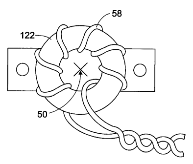
In the preferred embodiment, the transformer
is a toroidal ferrite core on a mounting bracket (see
FIGURE 2A) with seven turns of high voltage wire wound
around it (the number of turns can, of course, vary upon
demand). The seven turns comprise the secondary of the
transforming device 114 and are connected across damping
resistor 110. The primary is a single conductor 50
passing through the center of the core 12.2. Such a
construction effectively provides a single turn primary
with very low inductance. The capacitor 108 is mounted
directly to the switching device and presents a very low
inductance to the circuit 106.
With reference to FIGURE 2B, mounting bracket
126 is a stepped bracket to effectively raise the core
122 away from the support to which it is attached,
usually a cooling bus (not shown) of some sort, to allow
for adequate cooling of the core in view of the
temperatures it may reach during operation.
Another advantage of the transforming device
114 is that the effective primary resistance of the
circuit is the value of the resistor 110 divided by the
square of the turns ratio of the transformer 114. If
seven turns were employed, in this case it would be the
value of the secondary resistance divided by 49. A
consequent benefit of this construction is that the
secondary inductance is also divided by the same factor.
The resistor value can be se7_ected to give any desired
primary resistance while the transformer reduces the
insertion inductance by a facaor of approximately 49.
The significant advantage of this system is
that when the switching device current is initially
switched off, the capacitor 1.08 picks up 'the current and
there is only current in the resistor through the
secondary up to the point where the transformer core
Juw.l. ~Sx)s
CA 02267522 1999-03-29
- 9 -
saturates. It is thus intended in accordance with the
method of the invention that: core should be designed to
saturate quickly at the switching current levels. When
saturation does occur, the. resistor is thus out of the
circuit and the primary of t:he transformer looks like a
very low inductance short circuit to the bypassing
current. As the capacitor charges to the full applied
voltage, the current in the capacitor 108 and therefor
the transformer primary decreases so that the secondary
resistor 110 is effectively back in the circuit again.
In other words, the saturated core device goes out of
saturation so that the resistor can effectively dampen
the ringing and oscillations between the capacitor and
the inductance 104. Thus, a key advantage of the system
is that the saturation of the transformer core has no
effect on the ability of the resistor to damp
oscillations, or the capacitor to limit voltage spikes,
but does result in a significant reduction in the power
dissipated in the resistor b;y effectively taking the
resistor out of the circuit for the time period during
which the transformer is in saturation. For example, in
a common 10KHZ system, the resistor wattage dissipated
is about 173 watts compared to a system where the
resistor is merely serially connected to the capacitor
and where 1800 watts are dissipated by the resistor -
nearly a 90 percent improvemE~nt.
FIGURE 5 comprises a flowchart illustrating
the crucial steps in the implementation of the
invention. When the switching device 102 is opened at
step 140, the system current will bypass a switching
device into the network 106 t:o charge the capacitor 108.
The system thus provides a zero voltage switching of the
device 102 and thus avoids the undesired voltage spike.
Initially, since the transforming device is
not saturated, both the resistor 110 and 'capacitor 108
will effectively be in the circuit as shown at step 142.
Juh .',-t, 175
CA 02267522 1999-03-29
- 1.0 -
However, as will be seen later, the transformer device
114 quickly saturates so that the resistor 110 is only
in the circuit for a very short period of time. At
saturation, step 144, the resistor 110 is effectively
out of the circuit so that the current bypassing the
switching device does not dissipate power in the
resistor and solely charges up the capacitor 108. As
the capacitor becomes fully charged at step 146, the
current to the transformer is reduced so that the
ferrite core becomes unsaturated and the resistor is
reinserted into the system as at step 148.
The dramatic improvement in operational
advantages is best seen in reference to FIGURES 3A, 3B
and 3C. In FIGURE 3A, representing the system without
the network 106, channel 1 shows the IGBT collector
current from the time of turn off shown at 150 until
system voltage across the device is effectively reached,
at point 152. Channel 2 is 'the collector- emitter
voltage across the switch and it can be seen that the
voltage rises to approximately 1000 volts due to the
stray circuit inductance. Also, it can be seen that the
time interval where both the voltage and current are
relatively high is extended ;so that considerable power
is dissipated in the IGBT by the switching action of the
device.
FIGURE 3B shows comparable wave forms for a
system formed in accordance with the present invention.
Channel 1 shows the collector current going to zero and
channel 2 is the collector-emitter voltage rising at
turn off. An important difference to note with
reference to FIGURE 3A, is that the capacitor voltage
rises more slowly and has a :lower peak value. It
appears that the peak value :is in fact no more than 20
percent greater than the system voltage so that the
resulting voltage spike due i~o the switch turn off is
much safer than the system rE:presented in FIGURE 3A.
Wv Via. Ws
CA 02267522 1999-03-29
- 1.1 -
Also, the power dissipated by the IGBT in the
switching interval is considerably lower than the system
of FIGURE 3A. These features are shown more clearly in
FIGURE 3C which shows only the voltage rise on an IGBT
in the system including the saturable core transformer
of the subject invention. The collector-emitter voltage
shown is illustrated with indication of significant
events in the method of the invention. The time period
A denotes the interval where the transformer core is not
saturated and it can be appreciated that this is a very
short time relative to overall voltage rise. In period
B the transformer core is saturated and no power is
transferred to the resistor lby the secondary of the
transformer. This illustrates the significant reduction
in power losses achieved by vthe subject invention. For
a time period C the transformer core becomes unsaturated
and the secondary resistive :Load is in the circuit to
damp system oscillations and ringing.
With reference to l~IGURE 4 a more specific
embodiment of an inverter circuit is shown. A high-
voltage, high-current DC swii:ching circuit converts DC
power to AC power. The switching circuit or inverter 10
includes first and second IGBTs 12, 14 connected in
series. Each IGBT has an emitter 18, a collector 20 and
a base 22. The emitter 18 oi: the first IGBT 12 is
connected to the collector of: the second IGBT 14. The
collector of the first IGBT and the emitter of the
second IGBT are connected across the positive and
negative or source terminals 26, 28, respectively, of a
DC input.
A first diode 32 is connected in parallel
across the collector 20 and emitter 18 of the first IGBT
12. Analogously, a second diode 34 is connected in
parallel across the second IGBT 14. The diodes are
connected in a direction anti-parallel to the IGBTs.
That is, the diodes are connected to the IGBTs such that
the diode current flows in a direction opposite to the
miv =~. nx~x
CA 02267522 1999-03-29
- 7.2 -
IGBT current flow. These diodes function as clamping
diodes. When the collector-emitter voltage of the IGBT
rises to a certain level, the diode conducts current to
reduce the voltage and protect the IGBT from damage.
Connected in parallel to the first diode 32
and first IGBT 12 is a first ZVS capacitor 40 and a
first ferrite toroidal transformer 42 which are in
series. Analogously, connected in parallel to the
second diode 34 and second IGBT 14 is a second ZVS
capacitor 46 and a second ferrite toroidal transformer
48 which are in series. The ZVS capacitors supply a
load current during a switching interval in the circuit.
More specific to the configuration, each of
the ZVS capacitors 40, 46 are connected in series with a
primary winding 50 of the transformers 42, 48. The
first and second transformers are part of first and
second damping circuits 54, 56. The damping circuits
54, 56 minimize oscillations in the switching circuit 10
without consuming much electrical energy.
By way of background, a transformer is an
electrical component used to transfer electrical energy
from one AC circuit to another by magnetic coupling. In
general, a transformer consists of two multi turn coils
of wire placed in close proximity to cause the magnetic
field of one to link the other. One of the coils serves
as the primary winding and tlhe other serves as a
secondary winding. When the primary winding is
connected to alternating current, it produces an
alternating flux in the core. The flux generates a
primary electromotive force which is essentially equal
and opposite to the voltage ;supplied to it. It also
generates a voltage in the secondary winding. This
voltage generated in the secondary winding supplies
current to a device connected to the terminals of the
secondary winding. The current in the primary winding
is regulated to meet the power demand of the load
connected to the secondary winding. Thus, in normal
Juw ?a. W s
CA 02267522 1999-03-29
- .L 3 -
operation, current can be transferred from the primary
to the secondary electromagnetically. More importantly,
the electrical characteristics of an input current can
be altered to achieve desired electrical characteristics
in an output current. For example, transformers are
used to alter the following: voltage magnitude; current
magnitude; phase angle; impedance level and voltage
insulation level. Ordinarily, transformers are used in
inverters to change the voltage and current magnitude
between the inverter and a device driven by the
inverter. However, in the present invention, the
transformers 42, 48 serve another purpose.
With reference to FIGURE 2A, the primary
winding 50 of the transformer is a copper tube
approximately 2.5 cm in diameter. The copper tube
introduces very little inductance to the circuit. Each
of the secondary windings 58 of the first and second
transformers 42, 48 are connected across damping
resistors 60, 62, respectively. The secondary windings
are copper wire. The damping resistors dampen the
oscillations produced when the ZVS capacitors resonate
with the bus inductance.
The value of the resistance of the damping
resistor 60, 62 reflected back to the primary windings
58 is the resistor value divided by the square of the
turns ratio of the transformers. The value of the
damping resistors 60, 62 are chosen to give the desired
primary resistance. In the preferred embodiment, the
transformer has a 7-1 turns ratio. That is, the primary
winding consists of 1 turn of copper tube and the
secondary winding consists of 7 turns. Between the
IGBTs is an output terminal 66 which supplies
alternating current to a load (not shown). A ground
terminal 68 completes the circuit to the load.
As noted above, an advantage to this
configuration is that any secondary inductance is also
divided by the square of the turns ratio. Thus, while
iui, z.~. ms
CA 02267522 1999-03-29
- 14 -
the resistance is kept to a desired value, the
inductance in the primary is minimized.
Further, the watts in the damping resistor are
far lower than they would be if the resistor was
inserted in series in place of the primary winding. A
resistor directly in series with the capacitor would
dissipate much power during the charging and discharging
of the capacitor as well as during damping of
oscillations in the circuit. This waste of energy is
unnecessary.
In operation, the switching circuit is
supplied with DC power at input terminals 26, 28. The
bases 22 of the IGBTs are alternately biased with ~15 V.
More specifically, the base of the first IGBT 12 is
biased at +15 V to conduct current through the first
IGBT. Simultaneously, the base of the second IGBT 19 is
biased at -15 V to bar current through the second IGBT.
Thus, output terminals 66, 68 show a positive voltage.
Then, the biasing voltages to the bases 22 are stopped
or set to zero for an increment of time. After that,
the polarities on the bases are reversed and the first
IGBT is biased with -15 V and the second IGBT is biased
with + 15 V. Now, the output terminals show a negative
voltage. Again, the biasing voltages to the bases are
stopped for an increment of time. Then, the process is
repeated.
During the switching interval, i.e., during
the time that the biasing voltages to the bases are
zero, the load current is considered constant. This
load current is equal to the value of the current
switched out of the IGBT and into the ZVS capacitors.
Each capacitor supplies half the load current during
this time interval.
In the present embodiment, the transformer
saturates when the circuit is energized.' This
saturation limits the power coupled into the resistor
from the capacitor charging and discharging current.
!uly ~J, I~R
CA 02267522 1999-03-29
- 15 -
When the capacitor is charged up, the transformer
desaturates or comes out of saturation. Then, the
transformer-resistor combination or damping circuits 54,
56 acts to dampen the oscillations. Because
oscillations are minimized, the circuit is more energy
ef f icient .
In the preferred embodiment, the desired value
of primary resistance is approximately 400 milliohms.
As stated earlier, the resistance of the damping
resistor 62 as seen at the primary 50 is.a reduction of
the actual resistance of the resistor by the square of
the turns ratio of the transformer. Accordingly, the
damping resistor 62 is selected to be approximately: 7z x
400 x 10'3 = 19.6 ohms or 20 ohms. The actual inductance
of the 20 ohm resistor and associated leads is about 1
microhenry. However, placing the damping resistor into
the damping circuit 54, 56 reduces the perceived
inductance in the switching circuit to about 20
nanohenries.
With reference to FIGURE 1 and FIGURE 4, the
circuit 10 of the present invention successfully dampens
oscillations produced when the capacitors 40, 46
resonate with the circuit inductance. With reference to
FIGURE 3C, a graph of the collector-emitter voltage Vce
on one of the IGBTs 12, 14 versus time shows that the
voltage fluctuations are quickly dampened after the IGBT
is switched. The graph shows the dampened oscillations
of an embodiment in which a cross-sectional area of the
core of the damping transformers is 0.575 cmZ. The
following table presents the measurements in the circuit
corresponding to the results. of the graph of FIGURE 3C.
July 24, 1998
CA 02267522 1999-03-29
- 7.6 -
Table 1.
Characteristic Value
Biasing Frequency 10 kHz
Bus Voltage 658 V
Bus Inductance 150 nH
Damping Resistor 20 Ohms
ZVS Capacitor .5 ~F
Output Current 1000 A
Switching Current ~ 1413 A
Cross Sectional Area of Ferrite Core of 0.575 cm2
Transformer
Saturation Flux Density of the Core of the 4300 Gauss
Transformer
Total AC Capacitor Current at 10 kHz (RMS) 57 A
Capacitor Current (peak) 353 A
Collector-Emitter Voltage of IGBT (peak) 855 V
Resistor Current (peak) 50.4 A
Resistor Voltage (peak) 1009 V
Resistor Current (RMS) 2.94 A
Resistor Power (RMS) 173 W
Although the circuit is operative using two of
the same IGBTs, diodes, transformers, and damping
resistors, it is to be appreciated by one skilled in the
art that different values or types of components may be
used. Of course, the values or characteristics of the
components should be selected to achieve the desired
overall characteristics of the circuit and output
current.
Further, it is to be appreciated that the IGBT
may be replaced with other types of switching devices
such as MOSFETs, silicon-controlled rectifiers (SCRs)
and the like without departing from the scope of the
present invention. In addition, it is to be appreciated
lulp'_~1. 199X
CA 02267522 1999-03-29
i i
- 1.7 -
that the transformer-resistor or damping circuit of the
present invention may be used to dampen other types of
circuits.
Schematic illustrations of actual practical
configurations of inverter circuits are shown in FIGURES
7 - 9. FIGURE 7 shows a half bridge inverter with
series load circuit having first 72 and second 74
saturable core devices. FIGURE 8 is a full bridge
inverter with series load circuit having saturable core
devices 82, 84, 86, 88. FIGURE 9 is a full bridge
inverter with series parallel load circuit having
saturable core devices 92, 94, 96, 98.
The invention has been described with
reference to the preferred embodiments. Obviously,
modifications and alterations will occur to others upon
reading and understanding true preceding detailed
description. It is intended that the invention be
construed as including all ~:uch modifications and
alterations insofar as they come within the scope of the
appended claims or the equivalents thereof.
lulu =a. I~xn