Note: Descriptions are shown in the official language in which they were submitted.
CA 02267710 1999-03-24
1
LOW IMPEDANCE GRID-ANODE INTERACTION REGION
FOR AN INDUCTIVE OUTPUT AMPLIFIER
BACKGROUND OF THE INVENTION
1. Field of the Invention
The present invention relates to inductive output amplifiers having RF
modulation applied to an electron beam passing through a grid disposed
between an electron emitting cathode and an anode. More particularly, the
invention relates to a low impedance structure that prevents self-oscillation
of
the electron beam at a frequency determined in part by the resonant
frequency of the grid-anode interaction region.
2. Description of Related Art
It is well known in the art to utilize a linear beam device, such as a
klystron or travelling wave tube amplifier, to generate or amplify a high
frequency RF signal. Such devices generally include an electron emitting
cathode and an anode spaced therefrom. The anode includes a central
aperture, and by applying a high voltage potential between the cathode and
anode, electrons may be drawn from the cathode surface and directed into a
high power beam that passes through the anode aperture.
One class of linear beam device, referred to as an inductive output
amplifier, or inductive output tube (10T), further includes a grid disposed in
the
inter-electrode region defined between the cathode and anode. The electron
beam may thus be density modulated by applying an RF signal to the grid
relative to the cathode. After the density modulated beam is accelerated by
the anode, it propagates across a gap provided downstream within the
inductive output amplifier and RF fields are thereby induced into a cavity
coupled to the gap. The RF fields may then be extracted from the cavity in
the form of a high power, modulated RF signal.
As the modulated electron beam passes through the interaction region
CA 02267710 1999-03-24
2
defined between the grid and the anode, the modulated beam will radiate RF
energy from the interaction region if a high enough impedance is presented to
the modulated beam. Ideally, by avoiding reflections of the RF energy and
surrounding the grid-anode interaction region with "free space," a low
impedance is presented which minimizes RF radiation from the interaction
region. In practice, however, there is some leakage of RF radiation from the
grid-anode interaction region which can be harmful to other equipment and
persons in proximity to the device, and can couple to the cathode-grid space
causing oscillation. To prevent such undesirable leakage, the device is
ordinarily enclosed within a metallic housing which effectively shields the RF
radiation.
An unintended consequence of the housing, however, is that it
necessarily forms a cavity connected to the grid-anode interaction region. If
this grid-anode cavity presents a high impedance to the modulated electron
beam, the beam will radiate RF energy into the grid-anode cavity which may
be coupled back into the cathode-grid space. This can cause undesirable
regeneration of the beam modulation, i.e., a self-oscillation condition in
which
the electron beam is further modulated at a frequency determined by the
resonant frequencies of the cavities. The unwanted modulation of the
electron beam interferes with the RF signal which is desired to be amplified
by
the inductive output amplifier, and the radiated RF energy reduces the power
of the modulated beam, which reduces the gain of the amplifier. In extreme
cases, the self-oscillation can generate voltages high enough to damage the
amplifier.
An approach to overcoming this self-oscillation problem is to load the
cavity with lossy material in order to present a low impedance to the electron
beam over the band of frequencies at which the inductive output amplifier
operates. As known in the art, ferrite loaded silicon rubber material presents
a low impedance in the UHF and microwave frequency ranges and is capable
of standing off very high DC voltages on the order of several tens of
kilowatts.
CA 02267710 1999-03-24
3
A drawback of the use of such lossy material is that it is labor intensive,
and
hence costly, to apply the material to the grid-anode interaction region.
Moreover, the high voltage standoff characteristics of the material tend to
degrade over time, which reduces the performance of the inductive output
amplifier.
Thus, it would be desirable to provide an inductive output amplifier
having a low impedance grid-anode interaction region which avoids self-
oscillation. It would further be desirable to avoid the reliance upon lossy
ferrite material in reducing the impedance of the interaction region.
SUMMARY OF THE INVENTION
In accordance with the teachings of the present invention, an inductive
output amplifier is provided which has a low impedance grid-anode interaction
region. The low impedance is achieved without requiring lossy ferrite material
as in prior art systems, and serves to prevent RF radiation from the
interaction
region.
More particularly, a linear beam amplification device includes an axially
centered electron emitting cathode and an anode spaced therefrom. The
cathode provides an electron beam in response to a relatively high voltage
potential defined between the cathode and the anode. A control grid is
spaced between the cathode and anode for modulating the electron beam in
accordance with an input signal. A signal input assembly of the linear beam
amplification device comprises an axial input cavity into which the input
signal
is inductively coupled. The grid is electrically connected to the input
cavity.
An axially moveable tuning plunger is disposed within the input cavity with a
inductive coupling loop coupled to the tuning plunger allowing cooperative
movement therewith. A low impedance cavity is disposed coaxially with the
input cavity and is in electrical communication with an interaction region
defined between the grid and the anode. The grid-anode cavity and the input
cavity are separated by a common conductive wall, such that the outer wall
CA 02267710 2001-10-16
78267-3
4
(or outer conductor of a coaxial transmission line) of the
input cavity provides t:he inner wall (or center conductor)
of the grid-anode cavity.
In a first embodiment of the signal input
assembly, the grid-anode cavity is substantially enclosed by
an outer wall in which both the common wall and the outer
wall are comprised of a material having a relatively high RF
surface resistivity, such as iron. The high RF surface
resistivity tends to reduce the Q (quality factor) of the
1~~ grid-anode cavity, reducing the impedance of the grid-anode
cavity. The surface of the common wall within the input
cavity may be plated with a coating having a relatively low
RF surface resistivity, such as silver, so that the input
cavity has a high Q. The low impedance grid-anode cavity
1.'~ would extract only minimal amounts of RF energy from the
interaction region, resulting in negligible gain reduction
of the inductive output amplifier.
In a second embodiment of the signal input
assembly, the grid-anode cavity is provided with an
2() adjustable tuning structure. The tuning structure permits
the grid-anode cavity to be tuned to define a transmission
line having an electrical length equivalent to nA/4, where ~
is the wavelength of the input RF signal, and n is an even
integer. The tuning structure comprises an axially movable
25 choke disposed within the grid-anode cavity. The choke
provides an RF short that conducts RF currents while
maintaining a large DC voltage between the grid and the
anode. As a result, the transmission line would have zero
impedance at the interaction region, and would not extract
30 any RF energy from the modulated beam.
CA 02267710 2001-10-16
78267-3
4a
The invention may be summarized as in a linear
beam amplification device having an axially centered
electron emitting cathode and an anode spaced therefrom,
said cathode providing an electron beam in response to a
relatively high voltage potential defined between said
cathode and anode, a cc>ntrol grid spaced between said
cathode and anode for modulating the electron beam in
accordance with an input signal, a signal input assembly
comprises: an input cavity including means for inductively
coupling said input signal into said input cavity, said grid
being coupled to said input cavity; a moveable tuning
plunger disposed within said input cavity, said inductive
coupling means being coupled to said tuning plunger allowing
cooperative movement therewith; and a grid-anode cavity
adjacent with said input cavity and in communication with an
interaction region defined between said grid and said anode,
said grid-anode cavity presenting a relatively low impedance
to said interaction region.
A more complete understanding of the low impedance
grid-anode interaction region for an inductive output
amplifier will be afforded to those skilled in the art, as
well as a realization of additional advantages and objects
thereof, by a consideration of the following detailed
description of the preferred embodiment. Reference will be
2!~ made to the appended sheets of drawings which will first be
described briefly.
CA 02267710 1999-03-24
BRIEF DESCRIPTION OF THE DRAWINGS
Fig. 1 is a cross-sectional side view of an inductive output amplifier in
accordance with aspects of the present invention;
Fig. 2 is a cross-sectional side view of a first embodiment of a signal
5 input assembly for the inductive output amplifier;
Fig. 3 is a cross-sectional side view of a second embodiment of a
signal input assembly for the inductive output amplifier;
Fig. 4 is an enlarged cross-sectional side view of the inductive output
amplifier illustrating the cathode, grid and anode assemblies;
Fig. 5 is an end sectional view of the signal input assembly inductive
output amplifier; and
Fig. 6 is an enlarged cross-sectional side view of a cathode capsule
coupled to a signal input assembly of the present invention.
DETAILED DESCRIPTION OF THE PREFERRED EMBODIMENT
The present invention satisfies the need for an inductive output
amplifier having a low impedance interaction region between the grid and the
anode. The low impedance is achieved without requiring lossy ferrite material
as in prior art systems, and serves to prevent RF radiation from the modulated
electron beam to the grid-anode interaction region. In the detailed
description
that follows, like element numerals are used to describe like elements shown
in one or more of the figures.
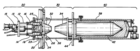
Referring first to Fig. 1, an inductive output amplifier is illustrated. The
inductive output amplifier includes three major sections, including an
electron
gun 20, a drift tube 30, and a collector 40. The electron gun 20 provides an
axially directed electron beam that is density modulated by an RF signal. The
electron gun 20 and the circuit used to couple the RF signal to the electron
gun is described in greater detail below.
The modulated electron beam passes through the drift tube 30, which
further comprises a first drift tube portion 32 and a second drift tube
portion
CA 02267710 2001-10-16
78267-3
6
34. The first and second drift tube portions 32, 34 each
have an axial beam tunnel extending therethrough, and are
separated by a gap. An RF transparent shell 36, such as
comprised of ceramic materials, encloses the drift tube
portions and provides ~~ partial vacuum seal for the device.
An output cavity (not shown) may be coupled to the RF
transparent shell 36 tc> permit RF electromagnetic energy to
be extracted from the modulated beam as it traverses the
gap.
The collector 40 comprises an inner structure 42
and an outer housing 38. The inner structure 42 has an
axial opening to permit. the spent electron beam to pass
therethrough and be collected after having traversed the
drift tube 30. The inner structure 42 may have a voltage
1.5 applied thereto that is depressed below the voltage of the
outer housing 38, and these two structures may be
electrically insulated from one another. As illustrated in
Fig. 1, the inner structure 42 provides a single collector
electrode stage. Alternatively, the inner structure 42 may
comprise a plurality of collector electrodes, each being
depressed to a different. collector voltage. An example of
an inductive output amplifier having a multistage depressed
collector is provided by U.S. Patent No. 5,650,751, to R.S.
Symons. The collector 40 may further include a thermal
control system for removing heat from the inner structure 42
dissipated by the impinging electrons.
The electron gun 20 is shown in greater detail in
Fig. 4, and includes a cathode 8 with a closely spaced
control grid 6. The cathode 8 is disposed at the end of a
cylindrical capsule 23 that includes an internal heater coil
25 coupled to a heater voltage source (described below).
CA 02267710 2001-10-16
78267-3
7
The cathode 8 is structurally supported by a housing that
includes a cathode terminal plate 13, a first cylindrical
shell 12, and a second cylindrical shell 16. The first and
second cylindrical she7_ls 12, 16 are comprised of
electrically conductive materials, such as copper, and are
axially connected together. The cathode terminal plate 13
permits electrical connection to the cathode 8, as will be
further described below. An ion pump 15 is coupled to the
cathode terminal plate 13, and is used to remove positive
ions within the electrc>n gun 20 that are generated during
the process of thermionic emission of electrons, as known in
the art.
The control grid 6 is positioned closely adjacent
to the surface of the cathode 8, and is coupled to a bias
1.5 voltage source (described below) to maintain a DC bias
voltage relative to the cathode 8, and to an RF input signal
to density modulate the electron beam emitted from the
cathode. The grid 6 may be comprised of an electrically
conductive, thermally rugged material, such as pyrolytic
graphite. The grid 6 is physically held in place by a grid
support 26. The grid support 26 couples the bias voltage
and RF input signal to the grid 6 and maintains the grid in
a proper position and spacing relative to the cathode 8. An
example of a grid support structure for an inductive output
amplifier is provided by U.S. Patent No. 5,990,622 to Shult,
et al.
The grid support 26 is coupled to the cathode
housing by a cathode-grid insulator 14 and a grid terminal
plate 18. The insulator 14 is comprised of an electrically
insulating, thermally conductive material, such as ceramic,
CA 02267710 2001-10-16
78267-3
7a
and has a frusto-conic~il shape. The grid terminal plate 18
has an annular shape, rind is coupled to an end of the
cathode-grid insulator 14 so that the cathode capsule 23
extends therethrough. The grid terminal plate 18 permits
electrical connection t.o the grid 6, as will be further
described below. The arid support 26 includes a cylindrical
extension that is axially coupled to the grid terminal plate
18. The diameter of the cylindrical extension of the grid
support 26 is greater than a corresponding diameter of the
1~ cathode capsule 23 so as to provide a space between the grid
6 and cathode 8 and hold off the ~C bias voltage defined
therebetween.
The leading edge of the first drift tube portion
32 is spaced from the grid structure 26, and provides an
1.'~ anode 7 for the electron gun 20. The first
CA 02267710 1999-03-24
8
drift tube portion 32 is held in an axial position relative to the cathode 8
and
grid 6 by an anode terminal plate 24. The anode terminal plate 24 permits
electrical connection to the anode 7, as will be further described below. The
anode terminal plate 24 is coupled to the grid terminal plate 18 by an
insulator
22 comprised of an RF transparent material, such as ceramic. The insulator
22 provides a portion of the vacuum envelope for the inductive output
amplifier, and encloses the interaction region defined between the grid 6 and
the anode 7 for which a low impedance structure is provided by this invention.
The insulator 22 is covered by a seal 38 having a corrugated surface to
increase the breakdown voltage path between the grid 6 and the anode 7.
The seal 38 may be comprised of silicon rubber material.
Referring now to Fig. 2, a first embodiment of a signal input assembly
for the inductive output amplifier is illustrated. The signal input assembly
comprises three concentric cylinders. An outer cylinder 62 provides an
external housing for the signal input assembly. An end plate 61 closes a first
end of the outer cylinder 62. The opposite end of the outer cylinder 62 has a
curved flange 63 that is coupled to the anode terminal plate 24 at an outer
peripheral portion thereof. The outer cylinder 62 is coupled to ground through
an insulated lead, as is the anode through the anode terminal plate 24. Air
inlet and exhaust ducts 65, 67 extend through the outer cylinder 62 to provide
a flow of cooling air to the electron gun. As will be further described below,
the outer cylinder 62 forms a portion of the grid-anode cavity.
An intermediate cylinder 64 is spaced within the outer cylinder 62 along
a common axis with the outer cylinder. Annular shaped spacers 71, 73
comprised of a non-electrically conductive material, such as ceramic, couple
the intermediate cylinder 64 to the outer cylinder 62. A first end of the
intermediate cylinder 64 terminates before reaching the end plate 61, leaving
a space therebetween. The opposite end of the intermediate cylinder 64 is
electrically connected to the grid terminal plate 18 through a socket 19
having
a frusto-conical shape.
CA 02267710 2001-10-16
78267-3
9
An inner cylinder 66 is spaced within the intermediate cylinder 64 along
the common axis. Annular shaped spacers 81, 83 comprised of a non-
electrically conductive material, such as ceramic, couple the intermediate
cylinder 64 to the inner cylinder 66. A first end of the inner cylinder 66
terminates at the same axial point as the first end of the intermediate
cylinder
64. The opposite end of the inner cylinder 66 is coupled to the cathode
terminal plate 13.
A high negative DC voltage, such as -32 kV, is applied by a cathode
voltage source labelled CATHODE to the cathode terminal plate 13 through
an electrically insulated lead. Similarly, current for the cathode heater 25
and
the ion pump 15 are supplied by sources labelled HEATER and ION PUMP,
respectively, through corresponding electrically insulated leads. A DC bias
voltage, such as -200 V relative to the cathode 8, is applied by a voltage
source labelled BIAS through an electrically insulated lead to the inner
cylinder 66.
Referring briefly to Fig. 6, the coupling between the inner cylinder 66
and the cathode terminal plate 13 is illustrated in greater detail. A sleeve
67
includes a plurality of conductive fingers 69 at an end thereof. The sleeve 67
is comprised of an electrically conductive material, such as copper, and
further includes a dielectric layer 85 wrapped around the periphery of the
sleeve. The sleeve 67 is disposed inside the inner cylinder 66 with the
dielectric layer 85 in direct contact with the inner surface of the inner
cylinder,
and the conductive fingers 69 in electrical contact with the edge of the
cathode terminal plate 1 ~~. The dielectric layer 85, such as comprised of
*KAPTON *TEFLON or nylon, operates as a choke (i.e., DC block or bypass
capacitor) to provide DC isolation between the cathode terminal plate 13 and
the inner cylinder 66, in . order to maintain a DC bias voltage between the
cathode 8 and the grid 6. The sleeve 67 and dielectric layer 85 extend in the
axial direction away from the cathode 8 by a length equal to approximately
~,/4, where ~, is the wavelength of the input RF signal in the dielectric
layer 85.
* Trade-mark
CA 02267710 1999-03-24
The conductive fingers 69 have a spring bias that maintains a positive
electrical connection with the cathode terminal plate 13. The conductive
fingers 69 are comprised of a flexible, electrically conductive material, such
as
copper. The use of the conductive fingers, rather than a rigid electrical
5 connection, facilitates simplified disassembly of the inductive output
amplifier
from the signal input assembly. It should be appreciated that similar
conductive fingers may also be utilized to maintain an electrical connection
between the socket 19 and the grid terminal plate 18, and between the curved
flange 63 and the anode terminal plate 24, shown in Fig. 2.
10 Returning now to Fig. 2, the intermediate cylinder 64 and the inner
cylinder 66 provide a coaxial transmission line which extends to the cathode-
grid interaction region, and the space between the cylinders defines an input
cavity for RF input signals provided to the inductive output amplifier. The
input cavity includes a coupling loop 82 disposed within a dome 84 having a
DC insulating capability, such as comprised of a ceramic material like
aluminum oxide (A1203). The DC insulating capability of the dome 84 is
necessary to permit the RF input signal having approximately zero DC voltage
to be coupled into the input cavity which is at a high negative DC voltage
(e.g., -32 kV). The coupling loop 82 is electrically connected through an
insulated coaxial line to receive the RF input signal (labelled RF INPUT)
which
is inductively coupled as an RF field into the input cavity. The RF fields
induced into the input cavity propagate through the socket 19 and grid
terminal plate 18 to result in an RF voltage being defined between the grid 6
and the cathode 8. As known in the art, the electron beam emitted by the
cathode 8 becomes density modulated by the RF input signal applied to the
input cavity.
The input cavity may be inductively tuned to a desired frequency range.
An annular shaped shorting plunger 68 is coupled to a threaded rod 72, and is
caused to move axially within the input cavity by operation of gears 78 and
77.
The gear 77 is coupled to a hand crank 79 that protrudes through a portion of
CA 02267710 1999-03-24
11
the outer cylinder 62. The gear 78 has an axially threaded bore that is in
mesh with the threaded rod 72. The gear 77 is in mesh with gear 78 such that
rotation of the hand crank 79 causes rotation of the gear 78, further causing
axial movement of the shorting plunger 68. The shorting plunger 68 is
comprised of an electrically conductive material, such as brass or aluminum,
to conduct both RF and DC currents between the intermediate cylinder 64 and
the inner cylinder 66 (i.e., between the outer conductor and center conductor
of the coaxial transmission line). The threaded rod 72 is comprised of an
electrically insulating material, such as nylon. A sleeve 75 extends axially
from the gear 78 to cover the threads of the threaded rod 72. It should be
appreciated that the position of the shorting plunger 68 within the input
cavity
may be controlled by other known mechanical systems, including but not
limited to motors, belts or pulleys.
The coupling loop 82 and dome 84 protrude through a portion of the
shorting plunger 68 and are moveable in the axial direction in cooperation
with
the shorting plunger. The dome 84 has an elongated portion 86 that extends
axially past the ends of the intermediate and inner cylinders 64, 66.
Alternatively, the elongated portion 86 may be formed of separate telescoping
elements that expand or contract as necessary to accommodate axial
movement of the shorting plunger 68. The insulated coaxial lead connected
to the coupling loop 82 passes through the elongated portion 86.
To move the shorting plunger 68 smoothly within the input cavity
without binding, it may be necessary to employ a plurality of threaded rods
similar to the threaded rod 72 shown in Fig. 2. The gear 78 has an axially
coupled pulley 74 that rotates in cooperation therewith. Similarly, a pulley
88
is provided concentrically around the elongated portion 86 of the dome 84. As
shown in Fig. 5, a plurality of pulleys 74~-744 may be provided, with each
pulley corresponding to an associated one of the threaded rods coupled to the
shorting plunger 68. The pulleys 74~-744 and 88 may be coupled by a belt 76
to coordinate operation of the threaded rods. The belt 76 may be comprised
CA 02267710 1999-03-24
12
of a high strength, light weight material, such as nylon, and may further
include a surface texture such as teeth to prevent slippage. An additional
pulley 106 coupled to a pivot arm 107 may be moved into engagement with
the belt 76. The additional pulley 106 can thereby be adjusted to take up any
slack in the belt 76.
The space defined between the outer cylinder 62 and the intermediate
cylinder 64 is referred to herein as a grid-anode cavity, as it provides a
parallel resonance that is directly coupled to the interaction region defined
between the grid 6 and the anode 7. In order to provide a low impedance to
the interaction region, the outer cylinder 62 and the intermediate cylinder 64
are comprised of a material having a high surface resistivity, such as iron or
steel. The high RF surface resistivity of the grid-anode cavity materials
produces a parallel resonance having low Q (i.e., quality factor) and
consequently a low impedance at the grid-anode interaction region. As a
result, any RF energy radiated into the grid-anode cavity will be damped out
quickly without regeneration into the cathode 8.
It is well known in the art that RF current is concentrated in a relatively
small surface region of a conductor, i.e., the "skin effect" of a conductor.
The
surface resistivity of a material is proportional to the square root of its
permeability divided by its conductivity. Both iron and steel are magnetic
metals having a relatively high permeability value and a low conductivity
value; hence, these materials have a relatively high surface resistivity. The
Q
of a resonator is the energy stored (U) divided by the power dissipated per
cycle (P~/w). The high surface resistivity of the grid-anode cavity materials
will
have high relative energy dissipation and therefore low Q. Since Q is also
proportional to the impedance (Zo), a reduction of Q equates to a reduction of
impedance.
More particularly, the characteristic impedance Zo of a transmission line
is given by the equation:
Z =
C
CA 02267710 1999-03-24
13
where L is the inductance per unit length of a transmission line and C is the
capacitance per unit length of the transmission line. The ratio of the shunt
resistance (RSH) to Q for any resonant circuit is given by the equation:
z
RSN -_ Vm
Q 2r.~U
in which Vm is the maximum voltage across the terminals at which RSH
appears, w is the angular frequency, and U is the energy stored in the line.
For a coaxial resonator having a length that is a multiple n of a quarter
wavelength (~,/4), the ratio of the shunt resistance (RSH) to Q reduces to:
RsH __ 4Zo
Q ~n
The Q of a coaxial resonator is proportional to Zo, and inversely proportional
to the series resistance RS per unit length, as follows:
Q - 2~Zo
~,RS
Accordingly, the high surface resistivity of iron or steel at the parallel
resonance in the grid-anode cavity should result in a low impedance, or shunt
resistance RSH, measured at the interaction region. Since the RSH/Q is
inversely proportional to length, it should be appreciated that the longer the
coaxial resonator, the lower the shunt resistance RSH will be.
As noted above, the intermediate cylinder 64 provides both the outer
conductor for the input cavity and the center conductor for the grid-anode
cavity. This is made possible by the "skin effect" discussed above. Since the
current at high frequencies is concentrated into a thin layer of a conductor,
the
conductive intermediate cylinder 64 actually acts as a barrier to prevent the
CA 02267710 1999-03-24
14
RF current in the input cavity from being conducted into the grid-anode
cavity,
and vice versa. To preclude dissipation of the RF current in the input cavity,
a
low surface resistivity coating is applied to the surfaces of the intermediate
cylinder 64 and the inner cylinder 66 facing into the input cavity. This may
be
accomplished by plating a layer of silver, or other material having high
conductivity and low permeability, onto the surfaces of the input cavity.
Referring now to Fig. 3, a second embodiment of a signal input
assembly for the inductive output amplifier is illustrated. The second
embodiment is generally similar in construction to the first embodiment
described above, and a description of like elements of the two embodiments
is therefore omitted. The signal input assembly of the second embodiment
differs with the addition of an adjustable choke which provides an RF short
circuit and a DC open circuit within the grid-anode cavity to define a
transmission line having an electrical length approximately equal to n~,/4,
where ~, is the wavelength of the input RF signal, and n is an even integer.
By
defining the transmission line to be an even multiple of a quarter wavelength
~,/4, the impedance at the interaction region will be zero.
The choke adjustment comprises a plurality of threaded rods 91
extending in an axial direction through the grid-anode cavity. The threaded
rods 91 are rotationally supported by a first bearing 89 disposed in spacer 71
and a second bearing 92 affixed to the curved flange 63. The threaded rods
91 are comprised of an electrically insulating material, such as nylon. An
annular choke assembly is carried by the threaded rods 91, and includes an
outer electrode portion 93, a dielectric portion 94, and an inner electrode
portion 95. The outer electrode portion 93 provides a broad, annular surface
spaced from the outer cylinder 62. A conductive finger 112 extends between
the outer electrode portion 93 and the outer cylinder 62 to provide an
electrical connection therebetween. The inner electrode portion 95 includes a
narrow surface that has a conductive finger 111 that comes into contact with
the intermediate cylinder 64, a threaded opening in mesh with the threaded
CA 02267710 1999-03-24
rods 91, and a wide surface that engages the dielectric portion 94. The
dielectric portion 94 envelopes the wide surface of the inner electrode
portion
95 and has an annular surface in contact with the outer electrode portion 93.
The dielectric portion 94 provides DC isolation between the outer
5 cylinder 62 and the intermediate cylinder 64 to maintain a large DC voltage
between the grid 6 anri the anocJe 7, and may be comprised of suitable
dielectric material such as KAPTON, TEFLON, nylon or epoxy. At the same
time, the dielectric portion 94 also provides an RF short circuit for
terminating
the grid-anode cavity. By positioning the adjustable choke axially within the
10 grid-anode cavity so that it lies on a series resonance position coinciding
with
an even multiple of a quarter wavelength ~,/4 from the interaction region
between the grid 6 and the anode 7, the impedance at the interaction region
will be zero and no voltage can be developed across it.
Axial movement of the choke is provided by gears 98 and 97. The
15 gear 97 is coupled to a hand crank 101 that protrudes through a portion of
the
outer cylinder 62. The gear 98 is coupled axially to one of the threaded rod
91. The gear 97 is in mesh with gear 98 such that rotation of the hand crank
101 causes rotation of the gear 98, further causing axial movement of the
adjustable choke. As with the shorting plunger 68 discussed above, it is
necessary to move the adjustable choke smoothly within the grid-anode cavity
without binding. Accordingly, a plurality of threaded rods similar to the
threaded rod 91 shown in Fig. 3 are employed. The gear 98 has an axially
coupled pulley 96~ that rotates in cooperation therewith.
As shown in Fig. 5, a plurality of pulleys 96~-964 may be provided, with
each pulley corresponding to an associated one of the threaded rods coupled
to the adjustable choke. The pulleys 96~-96a may be coupled by a belt 99 to
coordinate operation of the threaded rods 91. The belt 99 may be comprised
of a high strength, light weight material, such as nylon, and may further
include a surface texture such as teeth to prevent slippage. An additional
pulley 104 coupled to a pivot arm 105 may be moved into engagement with
CA 02267710 1999-03-24
16
the belt 99. The additional pulley 104 can thereby be adjusted to take up any
slack in the belt 99. It should be appreciated that the position of the
adjustable choke within the grid-anode cavity may be controlled by other
known mechanical systems, including but not limited to motors, belts or
pulleys.
Alternatively, the high voltage choke may be provided by disposing a
layer of dielectric material along the inner surface of the outer cylinder 62.
An
axially movable shorting plunger may be disposed in the grid-anode cavity in
the same manner as the adjustable choke described above with respect to
Fig. 3, although the shorting plunger is comprised of electrically conductive
materials, such as brass or aluminum, to conduct both RF and DC currents
between the intermediate cylinder 64 and the dielectric layer provided on the
outer cylinder 62. This way, the grid-anode cavity may be adjusted to define a
transmission line having an electrical length approximately equal to n~,/4,
where 7~ is the wavelength of the input RF signal, and n is an even integer.
The layer of dielectric material will maintain the large DC voltage between
the
grid 6 and the anode 7.
It should also be appreciated that the adjustable choke could be moved
slightly off the series resonance position so that the electron beam is
presented with a small inductive reactance at the axis of the interaction
region. Adjusted in this manner, the RF voltage across the interaction region
will be 90° out of phase with the beam current, so that electrons ahead
of the
electron bunch center will see a decelerating force while electrons behind the
center of the bunch will see an accelerating force. This adjustment will
overcome some of the normal debunching space charge forces and will
increase efficiency of the inductive output amplifier.
Having thus described a preferred embodiment of a low impedance
grid-anode interaction region for an inductive output amplifier, it should be
apparent to those skilled in the art that certain advantages of the within
described system have been achieved. It should also be appreciated that
CA 02267710 1999-03-24
17
various modifications, adaptations, and alternative embodiments thereof may
be made within the scope and spirit of the present invention. For example,
the input cavity and grid-anode cavity described above with respect to Figs. 2
and 3 were disposed in a coaxial configuration, but it should be appreciated
that radially disposed cavities could also be advantageously utilized.
The invention is further defined by the following claims.