Language selection

Search

Patent 2267817 Summary

Third-party information liability

Some of the information on this Web page has been provided by external sources. The Government of Canada is not responsible for the accuracy, reliability or currency of the information supplied by external sources. Users wishing to rely upon this information should consult directly with the source of the information. Content provided by external sources is not subject to official languages, privacy and accessibility requirements.

Claims and Abstract availability

Any discrepancies in the text and image of the Claims and Abstract are due to differing posting times. Text of the Claims and Abstract are posted:

  • At the time the application is open to public inspection;
  • At the time of issue of the patent (grant).
(12) Patent: (11) CA 2267817
(54) English Title: END PUMPED ZIG-ZAG SLAB LASER GAIN MEDIUM
(54) French Title: MEDIUM DE GAIN A PLAQUE ZIGZAG POUR LASER POMPE LONGITUDINALEMENT
Status: Deemed expired
Bibliographic Data
(51) International Patent Classification (IPC):
  • H01S 3/094 (2006.01)
  • H01S 3/0941 (2006.01)
  • H01S 3/06 (2006.01)
  • H01S 3/063 (2006.01)
  • H01S 3/16 (2006.01)
  • H01S 3/23 (2006.01)
(72) Inventors :
  • INJEYAN, HAGOP (United States of America)
  • HOEFER, CAROLYN S. (United States of America)
(73) Owners :
  • NORTHROP GRUMMAN CORPORATION (United States of America)
(71) Applicants :
  • TRW INC. (United States of America)
(74) Agent: GOWLING WLG (CANADA) LLP
(74) Associate agent:
(45) Issued: 2002-02-05
(22) Filed Date: 1999-03-31
(41) Open to Public Inspection: 2000-01-07
Examination requested: 1999-03-31
Availability of licence: N/A
(25) Language of filing: English

Patent Cooperation Treaty (PCT): No

(30) Application Priority Data:
Application No. Country/Territory Date
09/111,080 United States of America 1998-07-07

Abstracts

English Abstract


An optical amplifier which includes an
elongated slab of solid state lasing material, such as a
rare earth doped yttrium-aluminum-garnet (YAG). In
order to provide a relatively increased absorption
length and thus a higher overall efficiency, the optical
amplifier in accordance with the present invention
incorporates end pumping in which the pumped light is
coaligned with the amplified light resulting in
relatively longer absorption lengths and higher overall
efficiencies. The coaligned pumped sources are directed
to lateral faces of the slab which include windows,
formed from an insulating coating such as an anti-reflection
coating, at the pump wavelength. In order to
cause internal reflection of the pump beam along the
lasing axis, the end faces are formed at about a 45°
angle relative to the longitudinal axis which causes the
pumped light to be reflected within the slab co-axially
with a amplified light. In order to confine the
absorption of the pumped light to the center portion of
the slab, the opposing end portions of the slab may be
undoped while the center portion of the slab along the
longitudinal axis is doped. Such a configuration
provides relatively low residual thermal lensing with
virtually no birefringence.


Claims

Note: Claims are shown in the official language in which they were submitted.


-10-
The embodiments of the invention in which an exclusive
property or privilege is claimed are defined as follows:
1. An optical amplifier comprising:
an elongated slab of a solid state lasing material having a predetermined
cross-section defining opposing end faces and a plurality of lateral faces
therebetween,
a longitudinal axis defined between said opposing end faces generally parallel
to said
lateral faces;
means for enabling pumped light to be directed along an axis generally
parallel
to said longitudinal axis, said enabling means including a first footprint
formed on said
slab adjacent one of said opposing end faces, said footprint including a
coating disposed
on one of said end faces and a portion of lateral faces adjacent said one end
faces, said
one of said end faces configured at an angle relative to said longitudinal
axis, said
footprint enabling pump beams directed at an angle generally perpendicular to
the surface
of said lateral surface to be directed along said longitudinal axis; and
one or more sources of pump beams.
2. The optical amplifier as recited in claim 1, wherein said enabling means
includes a
second footprint formed on said slab adjacent the other of said opposing end
faces, said
footprint including a coating disposed on one of said end faces and a portion
of lateral
faces adjacent said one end faces, said one of said end faces configured at an
angle
relative to said longitudinal axis, said footprint enabling pump beams
directed at an angle
generally perpendicular to the surface of said lateral surface to be directed
along said
longitudinal axis.
3. An optical amplifier comprising:
an elongated slab of a solid state lasing material having a predetermined
cross-section defining opposing end faces and a plurality of lateral faces
therebetween,
a longitudinal axis defined between said opposing end forces generally
parallel to said
lateral faces;
means for enabling pumped light to be directed along an axis generally
parallel
to said longitudinal axis; and


-11-
one or more sources of pump beams;
said slab including means for limiting absorption of said pumped light along
said
slab.
4. The optical amplifier as recited in claim 3, wherein said limiting means
includes a
composite slab formed from two or more materials having two or more sections,
said two
sections defining a non-absorbing section and an absorbing section.
5. The optical amplifier as recited in claim 4, wherein said two or more
sections are
diffusion bonded defining one or more diffusion bond interfaces.
6. The optical amplifier as recited in claim 5, wherein one of said non-
absorbing sections
is formed adjacent a first end face.
7. The optical amplifier as recited in claim 6, further including a second non-
absorbing
section disposed adjacent a second end face, wherein said absorbing section is
disposed
in between said first and second non-absorbing sections.
8. The optical amplifier as recited in claim 7, wherein said non-absorbing
sections are
formed from undoped solid state lasing material.
9. The optical amplifier as recited in claim 8, wherein said undoped solid
state lasing
material is yttrium-aluminum-garnet (YAG).
10. The optical amplifier as recited in claim 8, wherein said absorbing
section is formed
from a doped solid state lasing material.
11. The optical amplifier as recited in claim 10, wherein said doped solid
state lasing
material is Y b doped YAG.
12. The optical amplifier as recited in claim 10, wherein said coating is an
anti-reflective
coating.


-12-
13. The optical amplifier as recited in claim 12, wherein said anti-reflective
coating is
selected for the wavelength of the pump beam.
14. The optical amplifier as recited in claim 1, wherein said one or more
sources of pump
beams includes one or more diode arrays.
15. An optical amplifier for amplifying light comprising;
an elongated slab of a solid state lasing material defining a longitudinal
axis and
opposing end faces configured at a predetermined angle relative to said
longitudinal axis
and a plurality of lateral faces;
a first window formed on one end of said slab disposed adjacent one end face
of
said slab, said window formed by applying a first coating along one end face
and a
portion of said lateral surfaces adjacent said end face; and
a first pump source.
16. The optical amplifier as recited in claim 15, wherein said source of
lasing material
is selected to have a relatively high index of refraction to cause the
amplified light to
reflect along said slab in a zig-zag pattern.
17. The optical amplifier as recited in claim 16, further including a second
window
formed on an opposing end of said slab window disposed adjacent an opposing
end face
of said slab and a second pump source, said window formed by applying a first
coating
along one end face and a portion of said lateral surfaces adjacent said end
face.
18. The optical amplifier as recited in claim 15, wherein said first coating
is formed from
an anti-reflection coating selected for the wavelength of said first pump beam
source.
19. The optical amplifier as recited in claim 17, wherein said second coating
is formed
from an anti-reflection coating selected for the wavelength of said second
pump beam
source.


-13-
20. The optical amplifier as recited in claim 15, wherein said slab is formed
from a
composite material defining one or more non-absorbing regions.
21. The optical amplifier as recited in claim 20, wherein said absorbing
region and one
or more non-absorbing regions are joined together by diffusion bonding.
22. The optical amplifier as recited in claim 21, wherein said absorbing
region is formed
from a doped host material.
23. The optical amplifier as recited in claim 22, wherein said doped host
material is
Y b:YAG.
24. The optical amplifier as recited in claim 21, wherein said one or more non-
absorbing
regions are formed from an undoped host material.
25. The optical amplifier as recited in claim 24, wherein said undoped host
material is
YAG.
26. The optical amplifier as recited in claim 15, wherein said first pump beam
source is
a diode array.
27. The optical amplifier as recited in claim 17, wherein said first and
second pump
sources are diode arrays.
28. The optical amplifier as recited in claim 27, wherein said optical
amplifier further
includes a lens assembly disposed between said first window and said first
pump source.
29. The optical receiver amplifier as recited in claim 20, further including a
coating
disposed on said lateral surfaces adjacent said absorbing region.
30. The optical amplifier as recited in claim 29, wherein said coating is an
evanescent
wave coating.


-14-
31. The optical amplifier as recited in claim 30, wherein said evanescent wave
coating
is M g F2.
32. The optical amplifier as recited in claim 30, wherein said evanescent wave
coating
is S i O2.
33. The optical amplifier as recited in claim 29, wherein said coating is a
thermally
conductive coating.
34. A master oscillator power amplifier comprising:
a master oscillator; and
an optical amplifier, said optical amplifier comprising:
an elongated slab of a solid state lasing material defining a longitudinal
axis and
opposing end faces configured at a predetermined angle relative to said
longitudinal axis
and a plurality of lateral faces;
one or more windows formed said slab disposed adjacent said end faces of said
slab, said window formed by applying a coating along said end face and a
portion of said
lateral surfaces adjacent said end face; and one or more pump sources.
35. A master oscillator comprising:
an input light source comprising:
a total reflector;
a Q switch; and
a polarizer;
an optical amplifier for receiving light from said input light source and
generating
an output beam; said optical amplifier comprising:
an elongated slab of a solid stat lasing material defining a longitudinal axis
and
opposing end faces configured at a predetermined angle relative to said
longitudinal axis
and a plurality of lateral faces;


-15-
one or more windows formed in said slab disposed adjacent said end faces of
said
slab, each said window formed by applying a coating along said end face and a
portion
of said lateral surfaces adjacent said end face; and
one or more pump sources; and an outcoupler for transmitting a portion of said
output beam.
36. The optical amplifier as recited in claim 10, wherein said doped solid
state lasing
material is T m doped YAG.
37. The optical amplifier as recited in claim 1, wherein said predetermined
cross section
is generally square.
38. The optical amplifier as recited in claim 1, wherein said predetermined
cross section
is generally rectangular.
39. The optical amplifier as recited in claim 22, wherein said doped host
material is
Tm: YAG.
40. The optical amplifier as recited in claim 33, wherein said thermally
conductive
coating is a soft metal.
41. The optical amplifier as recited in claim 40, wherein said soft metal is
indium.
42. The optical amplifier as recited in claim 40, wherein said soft metal is
gold.
43. The optical amplifier as recited in claim 27, wherein said optical
amplifier further
includes a lens duct disposed between said first window and said first pump
source.

Description

Note: Descriptions are shown in the official language in which they were submitted.


CA 02267817 1999-03-31
END PUMPED ZIGZAG SLAB LASER GAIN MEDIUM
BACKGROUND OF THE INVENTION
1. Field of the Invention
The present invention relates to an optical
amplifier for use, for example, in a high powered solid
state laser and more particularly to an optical
amplifier which includes an elongated slab of a solid
state lasing material, for example, a rare earth doped
yttrium-aluminum-garnet (YAG) crystal and a plurality of
diode arrays for exciting the solid state lasing
material to a relatively high energy metastable state,
wherein the pumping light is coaligned with the
amplified light resulting in relatively long absorption
lengths and thus higher overall efficiencies, making the
configuration particularly suitable for optical
amplifiers which use solid state lasing materials which
have a relatively low absorption length, such as Yb and
Tm .


CA 02267817 2001-08-24
-2-
2. Descri~,tion of the Prior Art
Optical ~~?npl ifiers are known which include an
elongated generally rectangular or square slab of a
lasing material, such as a rare earth doped yttrium-
aluminum-garnet (YAG) crystal. The slabs are formed
with a generally rectangular or square cross section
area defining a pair of opposing end faces and four
lateral faces. Material for the slab is selected to
have a relatively high index of refraction. The slab is
cooled with a cooling medium having a relatively low
index of refraction. This change in the index of
refraction at the slab coolant interface results in
incident light beams directed to one end face of the
slab being totally internally reflected through the slab
in a zig-zag manner. As such, the optical amplifiers
with such a configuration have become known as zig-zag
amplifiers. Examples of solid state lasers utilizing
such zig-zag amplifiers are disclosed in U.S. Patent
Nos. 4,730,324; 4,852,109 and 5,305,345.
In order to excite the solid state lasing
material to a relatively high energy metastable state,
various pumping sources, such as diode arrays are used,
for example, as disclosed in U.,S. Patent Nos.:
4,852,109; 4,949,346; 4,984,246; 5,271,031; 5,305,345;
5,317,585 and 5,351,251. In many known optical
amplifiers, the pumping sources are configured such that
the light from the pumping source is directed along a
lateral face of the slab i~ a direction generally
perpendicular to the longitudinal axis of the slab.
Examples of optical amplifiers with such a configuration
are disclosed in U.S. Patent Nos.: 4,127,827; 4,852,109;
5,271,031; 5,305,345; 5,646,773 and 5,651,021. Commonly
owned U.S. Patent No. 5,900,967 filed on December 12, 1996
discloses a configuration where a plurality of diode
arrays are directed along the lateral faces of the slab.
The system disclosed in '434


CA 02267817 1999-03-31
-3-
application utilizes diode arrays directed generally
orthogonal to a longitudinal axis of the slab as well as
diode arrays which are directed at an angle relative to
the, lateral faces to provide a general uniform energy
distribution in the slab. Such configurations, known as
side pumped configurations, unfortunately limit the
absorption length of the pumping light to just a few
millimeters. When such side pump configurations are
used with optical amplifiers which use a solid state
lacing material having a relatively low absorption
coefficient, such as Yb and Tm doped materials, a
relatively low absorption efficiency and, thus a lower
overall efficiency results. Thus, there is a need for
optical amplifiers capable of relatively longer
absorption lengths resulting in relatively higher
overall efficiencies.
f
smvrnzaRY of ~ nw;errrioN
Briefly, the present invention relates to an
optical amplifier which includes an elongated slab of
solid state lasing material, such as a rare earth doped
yttrium-aluminum-garnet (YAG) slab. In order to provide
a relatively increased absorption length and thus a
higher overall efficiency, the optical amplifier in
accordance with the present invention incorporates end
pumping in which the pumped light is coaligned with the
amplified light resulting in relatively longer
absorption lengths and higher overall efficiencies. The
coaligned pumped sources are directed to lateral faces
of the slab which include footprints or windows, formed
from anti-reflection coatings at the pump wavelength.
In order to cause internal reflection of the pump beam
along the lacing axis, the end faces are formed at about
a 45° angle relative to the longitudinal axis which
causes the pumped light to be reflected within the slab
co-axially with a amplified light. In order to confine
the absorption of the pumped light to the center portion


CA 02267817 1999-03-31
-4-
of the slab, the slab may be formed from a composite
material with the opposing end portions of the slab
formed from an undoped host material while the center
portion of the slab along the longitudinal axis is
formed from a doped host material. Such a configuration
provides relatively low residual thermal lensing with
virtually no birefringence.
DESCRIPTION OF THE DRAWINGS
The principles of the present invention may be
readily understood with reference to the following
specification and attached drawing wherein:
FIG. 1 is a plan view of an optical amplifier
in accordance with the present invention.
FIG. 2 is a diagram of an anamorphic lens
assembly and diode array for use with the present
invention.
FIG. 3 is a schematic diagram of the end pumped
optical amplifier in accordance with the present
invention in a resonator configuration.
FIG. 4 is similar to FIG. 3 where the optical
amplifier in accordance with the present invention is
used a master oscillator power amplifier (MOPA)
configuration. ,
DETAILED DESCRIPTION
The present invention relates to an optical
amplifier, generally identified with the reference
numeral 20. In accordance with an important aspect of
the invention, the optical amplifier 20 utilizes end
pumping. With such a configuration, the pumped light is
coaligned with the amplified light along a longitudinal
axis of the slab resulting in a relatively long
absorption length, thus providing relatively higher
overall efficiencies. The invention is particularly
suitable for optical amplifiers which utilize solid
state lasing material with relatively low absorption
coefficients, such as those materials using Yb and Tm


CA 02267817 1999-03-31
_5_
dopants. As will be discussed in more detail below, the
absorption of the pumped light may be confined to a
central region of the slab to reduce heating at the
opposing ends of the slab which are known to be
susceptible to warping.
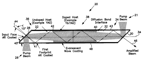
Referring to FIG. 1, the optical amplifier 20
includes a elongated slab 22 and a pair of pumped beam
sources 24 and 26. The elongated slab 22 is formed with
a generally rectangular or square cross section defining
a pair of opposing end faces 28 and 30 and four lateral
faces 32. As used herein, a longitudinal or lasing axis
34 is defined as an axis generally parallel to the
lateral surfaces 32 between the opposing end faces 28
and 30. A major axis is defined as a horizontal axis in
the direction of the zig-zag pattern while a minor axis
is defined to be a vertical axis generally perpendicular
to the major axis. Hoth the major and minor axis are
perpendicular to the longitudinal axis.
The slab 22 may be formed from a solid state lasing
material with a relatively high index of refraction to
cause internal reflection of the input beam in a
generally zig-zag pattern as illustrated in FIG. 1,
forming a so called zig-zag amplifier. Such zig-zag
amplifiers are known to allow brightness scaling by
allowing the input beam to average thermal gradients in
the slab effectively providing a homogeneous gain
medium. In order to reduce heating of the ends of the
slab 22, the slab 22 may be formed as a diffusion bonded
composite material. More particularly, along the
longitudinal axis 34 of the slab 22, the opposing end
portions 34 and 36 of the slab 22 can be formed from
undoped host materials, such as yttrium-aluminum-garnet
(YAG). These end portions 34 and 36 can be diffusion
bonded to a central portion 38 of the slab 22 formed
from a doped host material, such as Yb doped YAG
(Yb:YAG) forming two diffusion bond interfaces 40 and


CA 02267817 2001-08-24
-6-
42. Such diffusions bonding techniques are known in the art, for
example, as described in detail in U.S. Patent No. 5,441,803. SuC h a
configuration limits the absorption length to the center
portion 38 of the slab 22. ~y limiting the absorption
length to the certer portion 38 of the slab 22, heat
generated by the optical pumping is in the center
portion 38 and away from the end portions 34 and 36,
which are susceptible to warping. As mentioned above,
the pumped light is reflected through the slab 22. As
such the pump beams 24 and 26 may enter opposing lateral
faces 32 of the s7_ab 22 at opposing end portions 34 and
36, respectively, as generally shown in FIG. 1. In
order to enable t:he light into the slab 22, one or more
footprints or windows 41 and 43 may be formed on
opposing end portions 34 and 36. The windows 41 and 43
may be formed by way of a coating, such as an
antireflection coating selected for the wavelength of
the pump beams 24 and 26. As shown in FIG. 1, the
antireflection coating is disposed on the lateral face
32 as well as the opposing end faces 28 and 30 and
thereby reducing losses of the input beam and pump beam.
The pump beams 24 and 26 are directed to opposing
lateral faces 32 at opposing end portions 34 and 36 of
the slab 32. As shown in FIG, 1, the pump beams 24 and
26 are totally reflected from the opposing end face 28
and 30 so that the pump beams are coaligned with the
longitudinal axis 34. By utilizing the composite slab
22 as discussed above, the absorption length of the slab
22 is limited to the central portion 28.
An input light beam 44 is directed to one end face
28 at a relatively small angle, for example, less than
10° relative to the normal of the end face. By
confining the angle of incidence of the input angle 44
and selecting a material having a relatively high index
of refraction, t:he input light beam 44 is totally


CA 02267817 2001-08-24
_7_
reflected along !Yhe slab 22 in a generally zig-zag
pattern as shown and is out coupled as an amplified beam
46 from the opposing end face 30. The zig-zag pattern
across the slab temperature gradients combined with
uniform pumping ~y the guided diode light and insulated
slab edge results in relatively low thernial tensing with
virtually no birefringence.
It is known in the art that pumping of the slab
22 results ir_ increased temperature in the area where
the pump light is absorbed. As mentioned above, pump
beams, for example, from diode arrays, are directed
generally perpendicular to the end faces 32 through the
windows or footprints 41 and 43 and reflected from the
opposing end faces 28 and 30 to cause the pump beam to
be directed along the longitudinal axis 34. In order to
cool the slab 22, various cooling methods can be used.
Hoth conduction and convection cooling systems are
suitable. An example of a conduction cooling system is
to attach the slab 22 to a high intensity impingement
cooler, for example, as manufactured by Thermal Electron
in San Diego, California or SDL, Inc. in San Jose
California.
To minimize the thermal resistance between the
slab 22 and the coolers, a thin layer of a thermally
conductive material such as a soft metal, such as indium
or gold as generally illustrated in FIGS. 3 and 4, may
be used. During assembly, the cooler/indium/slab
assembly may be held under pressure at elevated
temperatures, approximately 150°C to flow the indium and
eliminate contact resistance. For direct or connective
cooling, the slab 22 may.sealed in the dead zones with a
thin Layer of turbulent coolant flowing over the slab
faces to remove heat as discussed in detail in U.S.
Patent No. 5,646,773.
An exemplary convection cooling system is disclosed for
example, in commonly owned U.S. Patent No. 5,646,773,


CA 02267817 2001-08-24
-8-
In the case of convection and conduction
cooling, the lateral faces 32 of the slab 22 are coated
with a dielectric material which serves as an evanescent
wave coating 48 to preserve total internal reflection.
As shown in FIG. 1, the evanescent wave coating 48 may
extend from one end face 29, 30 to a region slightly
beyond the diffusion bond interface 42, adjacent to the
opposing end face. The evanescent wave coating 48
allows the slab 22 to be in directly adhered to the
impingement cooler. A thick layer (2-4~,m) of MgF2 or
SiOz may be used as the evanescent wave coating 48.
High power diode arrays 56, for example, with a
diode array cooler 57, may be used to generate the pump
IS beams 24 and 26. Efficient pumping of the slab 22 may
be achieved by using a suitable anamorphic lens assembly
50 as generally illustrated in FIG. 2. The anamorphic
lens assembly in~~ludes a pair of lenses 52 and 54,
disposed between a diode array 56 and the windows 41 and
43 on the slab 22. The diode arrays 56 may include a
plurality of star_ked diode bars 58 with individual
microlenses 60. The microlenses 60 reduce the
divergence of the fast axis of the bars 58 to
approximately 1° while the slow axis may have a full
angle divergence on the order of 7°. Hy using the
anamorphic lens assembly 50, the output of the diode
array 56 can be imaged onto the input area on the
windows 41 and 43 of the slab 22 such that a 2 X 1 cm
diode array may be imaged ~on an area as small as 2 X 2
mm .
Alternatively, a lens duct may be used in place
of the anamorphic: lens assembly 50. A suitable lens
duct is disclosed in U.S. Patent No. 5,307,430.
The optical amplifier 20 in accordance with the
present invention may be used to form a master


CA 02267817 1999-03-31 '
_g_
oscillator power amplifier (MOPA). In this embodiment
as illustrated in FIG. 3, a master oscillator 72 is
directed to an input end face 28 of the slab 22. The
master oscillator may be, for example, as discussed and
illustrated with respect to FIG. 4 below. As discussed
above, the input beam to the end face must be less than
10° relative to the normal axis to the end face.
As illustrated in FIG. 4, the optical amplifier
20 may be used to form a master oscillator 74. In this
embodiment, an input beam is reflected from a total
reflector 76 by way of a Q switch 78 and polarizer 80 to
an input end face 28 of the slab 22. The output beam is
directed to a outcoupler 84 which transmits an out-
coupled output beam 86.
Obviously, many modifications and variations of
the present invention are possible in light of the above
teachings. Thus, it is to be understood that, within
the scope of the appended claims, the invention may be
practiced otherwise than as specifically described
above.
What is claimed and desired to be covered by a
Letters Patent is as follows:

Representative Drawing
A single figure which represents the drawing illustrating the invention.
Administrative Status

For a clearer understanding of the status of the application/patent presented on this page, the site Disclaimer , as well as the definitions for Patent , Administrative Status , Maintenance Fee  and Payment History  should be consulted.

Administrative Status

Title Date
Forecasted Issue Date 2002-02-05
(22) Filed 1999-03-31
Examination Requested 1999-03-31
(41) Open to Public Inspection 2000-01-07
(45) Issued 2002-02-05
Deemed Expired 2008-03-31

Abandonment History

There is no abandonment history.

Payment History

Fee Type Anniversary Year Due Date Amount Paid Paid Date
Request for Examination $400.00 1999-03-31
Registration of a document - section 124 $100.00 1999-03-31
Application Fee $300.00 1999-03-31
Maintenance Fee - Application - New Act 2 2001-04-02 $100.00 2001-01-09
Final Fee $300.00 2001-11-08
Maintenance Fee - Patent - New Act 3 2002-04-01 $100.00 2002-03-04
Maintenance Fee - Patent - New Act 4 2003-03-31 $100.00 2003-02-04
Registration of a document - section 124 $50.00 2003-09-22
Maintenance Fee - Patent - New Act 5 2004-03-31 $200.00 2004-03-04
Maintenance Fee - Patent - New Act 6 2005-03-31 $200.00 2005-03-04
Maintenance Fee - Patent - New Act 7 2006-03-31 $200.00 2006-03-01
Owners on Record

Note: Records showing the ownership history in alphabetical order.

Current Owners on Record
NORTHROP GRUMMAN CORPORATION
Past Owners on Record
HOEFER, CAROLYN S.
INJEYAN, HAGOP
NORTHROP GRUMMAN SPACE & MISSION SYSTEMS CORP.
TRW INC.
Past Owners that do not appear in the "Owners on Record" listing will appear in other documentation within the application.
Documents

To view selected files, please enter reCAPTCHA code :


To view images, click a link in the Document Description column. To download the documents, select one or more checkboxes in the first column and then click the "Download Selected in PDF format (Zip Archive)" or the "Download Selected as Single PDF" button.

List of published and non-published patent-specific documents on the CPD .

If you have any difficulty accessing content, you can call the Client Service Centre at 1-866-997-1936 or send them an e-mail at CIPO Client Service Centre.


Document
Description 
Date
(yyyy-mm-dd) 
Number of pages   Size of Image (KB) 
Claims 2001-08-24 6 228
Description 2001-08-24 9 396
Cover Page 2002-01-14 1 57
Cover Page 1999-12-22 1 53
Abstract 1999-03-31 1 36
Description 1999-03-31 9 387
Claims 1999-03-31 6 232
Drawings 1999-03-31 3 59
Representative Drawing 1999-12-22 1 16
Representative Drawing 2002-01-14 1 19
Fees 2002-03-04 1 30
Assignment 2003-09-22 72 4,813
Correspondence 2001-11-08 1 30
Assignment 1999-03-31 5 196
Prosecution-Amendment 2001-02-26 2 48
Prosecution-Amendment 2001-08-24 12 496