Note: Descriptions are shown in the official language in which they were submitted.
CA 02268115 1999-04-07
WO 98/26367 PCT/US97/20628
.. _1_
Description
ANTI-COUNTERFEIT VALIDATION METHOD AND SYSTEM
FOR ELECTRONIC CASH CARDS
TECHNICAL FIELD
The present invention relates to optical
security methods and apparatus for smart cards.
BACKGROUND ART
Electronic commerce is a method of doing
business transactions at a distance and making payments
electronically. The Internet, interactive networks and
cable and ATM machines are being utilized for electronic
commerce. The smart card containing a microchip with
semiconductor memory or microprocessor and memory was
invented about 18 years ago. During the past few years
there have been efforts to store monetary value on such
cards which have been called electronic wallets or
electronic purses. One of the better known cash card
systems is known as the Mondex card or Mondex electronic
cash smart cards which is owned by a group of banks and
credit card issuers. The Mondex card system and other
electronic cash smart cards were promoted as being
tamperproof. This attracted the interest of Bell
Communications Research (Bellcore) and the Weizmann
Institute and the Technion Institute which undertook
research to break the microchip security codes. They
were successful and reported their results in November
1996 that a valid electronic cash smart card with its
security codes can be duplicated, that is, counterfeited.
The problem facing the financial institutions was how
they could proceed with their plans to build an
electronic commerce industry through the Internet and
other networks when a principal tool, the electronic cash
smart card, was subject to counterfeiting.
CA 02268115 1999-04-07
WO 98/263b7 PCT/US97/20628
-2-
It is the object of the present invention to
devise a method and apparatus to inhibit the counterfeit-
ing of electronic cash smart cards.
DISCLOSURE OF THE INVENTION
The above objective has been met by a smart
card having a pre-formatted optical memory stripe bonded
to a plastic wallet-size substrate containing an
electronic cash microchip. The data tracks on the
optical memory stripe would be typically separated by 12
microns or 7.5 microns and would use recorded spots from
one to three microns in diameter. The card validation
data would comprise one thousand to one million of
recorded spots.
The validation data could be recorded with a
lower power laser apparatus by the bank or card issuer.
The validation data could also be recorded by the card
manufacturer onto the card using either a low power laser
or photolithographic techniques. Under some security
arrangement the validation could comprise recordings of
both the card manufacturer and the card issuer.
Whereas counterfeiters have access to customer
microchip manufacturing, there are only three optical
memory card manufacturers in the world. Each of these
three optical card manufacturers uses different and
distinguishing optical storage media. It requires about
$20 million and a high degree of technical knowhow to
build such a manufacturing plant. One such optical
memory card manufacturing plant exists in the U.S.A. and
two in Japan using security controls on the manufacturing
and distribution of the optical memory portion of the
card and on the laser writing apparatus such technology
can be kept out of the hands of the counterfeiters.
The validation data must be read optically and
utilized to thwart the counterfeiter. The method and
apparatus for reading the data will involve either CCD
arrays, other photodetector arrays or a single photo-
detector. The photodetector array could be of the linear
CA 02268115 2004-11-26
7 0622-67
3
variety or a single photodetector could be used, in both
cases the card would have to be in motion. In the case of a
two-dimensional photodetector array the card would not
require motion but instead the validation data images would
be scanned electronically. The use of two dimensional CCD
arrays to read data from an optical memory is described in
U.S. Pat. Nos. 4,745,484 and 4,864,630. The use of a linear
photodetector array to read optical memory is described in
U.S. Pat. No. 4,634,850. The use of a single photodetector
to read an optical memory is described in U.S. Pat. Nos.
4,500,777 and 4,544,835.
The validation data on the electronic cash smart
card is read by a reading device containing photodetectors
and electronically compared against reference data stored
locally to determine the validity of the electronic cash
card before funds are dispersed. These functions could be
carried out in a public kiosk as part of an electronic
commerce system. Just as a vending machine would reject
counterfeit coins or currency the public kiosk would reject
a card not containing key elements of the validation data.
Validation data would also be confirmed by the
recipient of the money transfer. The validation data from
the payor's kiosk would be transmitted to the payee's kiosk
where the validation data would be compared against
reference data to determine its validity before the money
transfer would be accepted by the payee.
According to one broad aspect of the invention,
there is provided a method of validating an electronic cash
card comprising, bonding an optical memory stripe to the
card, recording optical validation data on a specific
location on the optical memory stripe by forming a plurality
of spots in a surrounding field of a reflective layer
CA 02268115 2004-11-26
70622-67
3a
in a laser recording material, recording reference
validation data in a card reading device, reading optical
data on the optical stripe at the location specified for the
validation data by detecting an optical reflective contrast
between the surrounding field and the recorded spots,
comparing the optical and reference validation data in the
reading device, accepting or rejecting the electronic cash
card depending upon whether the optical validation data
matches the reference validation data.
BRIEF DESCRIPTION OF THE DRAWINGS
Fig. 1 is a top plan view of a smart card in
accord with the present invention.
Fig. 2 is an enlarged view of a thin optical
recording strip on a card in accord with Fig. 1.
Fig. 3 is a plan view of optical apparatus for in-
situ writing on the optical recording material of the card
of Fig. 1.
CA 02268115 1999-04-07
WO 98/26367 PCT/LTS97/20628
-4-
BEST MODE FOR CARRYING OUT THE INVENTION
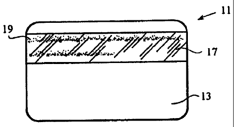
With reference to Fig. 1, a smart card 11 is
illustrated having a size common to most credit cards.
The card's substrate material 13 is a dielectric, usually
a plastic such as polyvinyl chloride or similar material
carrying a chip inside, for example, as shown in U.S.
Pat. Nos. 5,365,655 and 5,134,773. Polycarbonate is
preferred. The surface finish of the base should have
low specular reflectivity, preferably less than 10~.
Substrate 13 carries strip 17. The strip is
typically 16 or 35 millimeters wide and extends the
length of the card. Alternatively, the strip may have
other sizes and orientations. The strip is relatively
thin, typically 60-200 microns, although this is not
critical. Strips of laser recording material may be
applied to both sides of card 11. The strip may be
applied to the card by any convenient method which
achieves flatness.
The strip 17 is adhered to the card with an
adhesive and is covered by a transparent laminating sheet
76 seen in Fig. 3 which serves to keep strip 17 flat, as
well as protecting the strip from dust and scratches.
Sheet 76 is a thin, transparent plastic sheet laminating
material or a coating, such as a transparent lacquer.
The material is preferably made of polycarbonate plastic.
The high resolution laser recording material
which forms strip 17 may be any of the reflective
recording material which have been developed for use as
direct read-after-write (DRAW) optical disks, so long as
the materials can be formed on thin substrates. An
advantage of reflective materials over transmissive
materials is that the read/write equipment is all on one
side of the card, the data storage capacity is doubled
and automatic focus is easier. For example, the high
resolution material described in U.S. Pat. No. 4,230,939
issued to de Bont, et al. teaches a thin metallic
recording layer of reflective metals such as Bi, Te, Ind,
Sn, Cu, Al, Pt, Au, Rh, As, Sb, Ge, Se, Ga.
CA 02268115 1999-04-07
WO 98/26367 PCT/US97/20628
-5-
Materials which are preferred are those having
high reflectivity and low melting point, particularly Cd,
Sn, T1, Ind, Bi and amalgams. Suspensions of reflective
metal surfaces in organic colloids also form low melting
temperature laser recording media. Silver is one such
metal. Typical recording media are described in U.S.
Pat. Nos. 4,314,260, 4,298,684, 4,278,758, 4,278,756
and 4,269,917, all assigned to the assignee of the
present invention.
The laser recording material which is selected
should be compatible with the laser which is used for
writing on it. Some materials are more sensitive than
others at certain wavelengths. Good sensitivity to
infrared light is preferred because infrared is affected
least by scratches and dirt on the transparent laminating
sheet. The selected recording material should have a
favorable signal-to-noise ratio and form high contrast
data bits with the read/write system with which it is
used.
The material should not lose data when
subjected to temperatures of about 180°F (82°C) for long
periods. The material should also be capable of
recording at speeds of at least several thousand
bits/sec. This generally precludes the use of materials
that require long heating times or that rely on slow
chemical reactions in the presence of heat, which may
permit recording of only a few bits/sec. A large number
of highly reflective laser recording materials have been
used for optical data disk applications.
Data is recorded by forming spots in the
surrounding field of the reflective layer itself, thereby
altering the reflectivity in the data spot. Data is read
by detecting the optical reflective contrast between the
surrounding reflective field of unrecorded areas and the
recorded spots. Spot reflectivity of less than half the
reflectivity of the surrounding field produces a contrast
ratio of at least two to one, which is sufficient
contrast for reading. Greater contrast is preferred.
CA 02268115 1999-04-07
WO 98/26367 PCT/US97/20628
-6-
Reflectivity of the strip field of about 50~ is preferred
with reflectivity of a spot in the reflective field being
less than 10%, thus creating a contrast ratio of greater
than five to one. Alternatively, data may also be
recorded by increasing the reflectivity of the strip.
For example, the recording laser can melt a field of dull
microscopic spikes on the strip to create flat shiny
spots. This method is described in SPIE, Vol. 329,
Optical Disk Technology (1982), p. 202. A spot
reflectivity of more than twice the surrounding spiked
field reflectivity produces a contrast ratio of at least
two to one, which is sufficient contrast for reading.
Data strip 17 is intended to provide a data
record and has digital information indicia. Digital
machine readable data is written in individual tracks
extending in a longitudinal direction, as indicated by
the spot patterns 19 and these spot patterns are ana-
logous to sound track on a film, except that the data
tracks contain a much higher density of information and
are usually read in reflection, rather than in transmis-
sion, typically by a CCD array. The information density
is greater because each of the spots in the spot pattern
is approximately 5-10 microns in diameter with a spacing
of about 5-10 microns between spots. The spots are
recorded by a laser in the usual way, for example as
shown in U.S. Pat. No. 4,278,756 to Bouldin et al.
With reference to Fig. 2, a card substrate 70
carries an optional secondary substrate 72 which is a
thin flexible material, only a few mils thick carrying a
laser recording material 74. The secondary substrate 72
is adhered to the primary substrate 70 by means of an
adhesive or sticky substance, similar to dry adhesives
found on tape. The laser recording material may be any
of the materials previously discussed. A protective
coating 76 is applied over the laser recording material.
A laser writing apparatus is illustrated in
Fig. 3 which illustrates the side view of the lengthwise
dimension of the medium of Fig. 1 consisting of a data
CA 02268115 1999-04-07
WO 98/26367 PCT/US9?/20628
_7_
strip having digital information in combination with
microscopic visually readable information on a card. The
data strip portion 41 of the medium is usually received
in a movable holder 42 which brings the strip into the
trajectory of a laser beam. A laser light source 43,
preferably a pulsed semiconductor laser of infrared
wavelength emits a beam 45 which passes through
collimating and focusing optics 47. The beam is sampled
by a beam splitter 49 which transmits a portion of the
beam through a focusing lens 51 to a photodetector 53.
The detector 53 confirms laser writing. The beam is then
directed to a first servo controlled mirror 55 which is
mounted for rotation along axis 57 in the direction
indicated by arrows B. The purpose of the mirror 55 is
to find the lateral edges of the data strip in a coarse
mode of operation and then in a fine mode of operation
identify data paths or character sites which exist
predetermined distances from the edges.
From mirror 55, the beam is directed toward a
mirror 61. This mirror is mounted for rotation at pivot
63. The purpose of mirror 55 is for fine control of
motion of the beam along the length of the data strip.
Coarse control of the lengthwise portion of the data
strip relative to the beam is achieved by motion of the
movable holder 42. The position of the holder may be
established by a linear motor and used by a closed loop
position servo system of the type used in magnetic disk
drives. Reference position information may be
prerecorded on the card so that position error signals
may be generated and used as feedback in motor control.
Upon reading one data path, the mirror 55 is slightly
rotated. The motor moves holder 42 lengthwise so that
the path can be read again, and so on.
For writing microscopic visually readable
information, mirror 55 is used to identify character
sites at predetermined distances from the edges. Mirror
57 moves the scanning beam lengthwise from character site
to character site. Upon reading one row of character
CA 02268115 2004-11-26
70622-67
8
sites, mirror 55 is slightly rotated. Within a character
site, mirrors 55 and 57 cooperate to move the beam in either
a zig-zag pattern or a raster-like pattern. Laser spots are
written at designated locations within a character site to
form a character. When one character is written mirrors 55
and 57 move the beam to the next character site.
As light is scattered and reflected from spots in
the laser recording material, the percentage of reflected
light from the incident beam changes relative to surrounding
material where no spots exist. The incident laser beam
should deliver sufficient laser energy to the surface of the
recording material to create spots in the data writing mode,
but should not cause disruption of the surface so as to
cause difficulty in the lower beam power data reading mode.
The wavelength of the laser should be compatible with the
recording material to achieve this purpose. In the read
mode, power is approximately 5o to 10% of the recording or
writing power.
Differences in reflectivity between a spot and
surrounding material are detected by a CCD array 65, either
a linear array or area array. Light is focused onto the
detector 65 by beam splitter 67 and focusing lens 69. The
number of detector elements per track would be approximately
three elements to create a reading redundancy. The surface
would be illuminated with low-cost light-emitting diodes
generating power primarily in the near infrared to match the
sensitivity spectrum of the photodetector array.
Once a card is prepared, with either prerecorded
information on the optical strip or with laser written
information, the extended information must be sufficiently
complex to prevent easy replication. For example,
CA 02268115 2004-11-26
70622-67
8a
a pattern of one million spots, being the digital
representation of a random number, might be an
authentication "password" or validation data. A group of
numbers, representing a card serial number, date of card
issuance, geographical location of issuer and types of
purchases not permitted could be encoded with the spots.
s
CA 02268115 1999-04-07
WO 98/26367 PCT/US97/2062$
.. -g-
When this password or verification data is matched with
another password associated with an electronic reader, a
verification signal is generated, indicating an
authentic card. The reader may be linked electronically
with a password server or the passwords may be stored in
a memory local to the reader.
The passwords may be prerecorded by the card
manufacturer, using a photolithography process or a laser
process, as described above. Alternatively, the password
may be written by a card-issuing agency or by both the
card manufacturer and the card-issuing agency. Passwords
or validation data could be limited in use to a group of
issuers.