Note: Descriptions are shown in the official language in which they were submitted.
CA 02268575 1999-04-06
- 1 -
CIRCUIT BREAKER
The present invention relates to a circuit breaker for
disconnecting a load from an AC power supply in the event
of a circuit fault.
BACKGROUND OF THE INVENTION
Circuit breakers for use in an AC power/load circuit are
generally known. A typical circuit breaker includes a
transformer for monitoring the current before and after
flowing through the load and inducing a voltage when the
io current is unbalanced, for example, in the case of an earth
leakage fault, a voltage comparator for comparing the
induced voltage with a reference voltage and for generating
a signal indicative of the voltage difference, and a switch
for disconnecting the load from the power supply if the
i5 voltage difference is unacceptably large.
The invention seeks to provide an improved circuit breaker.
~UNIMARY OF THE INVENTION
According to the invention, there is provided a circuit
breaker for use in a power/load circuit formed by a three-
2o phase AC power supply and a load connected to the power
supply by means of three live power lines, which circuit
breaker comprises a tripping circuit including normally-
CA 02268575 1999-04-06
- 2 -
open switches connected in series with the respective power
lines facing the power supply, a transformer having at
least three balanced primary windings connected
subsequently in series along the respective power lines and
a secondary winding, a voltage comparator connected to the
secondary winding for comparing a voltage induced in the
transformer with a reference voltage and then in the event
of a leakage fault in the power/load circuit providing a
tripping signal for the tripping circuit to open the
io switches in order to disconnect the load from the power
supply, and a circuit path comprising a combined voltage
sensor/comparator and extending across opposite sides and
externally of the transformer for sensing and comparing two
phase-to-phase voltages of the power lines with each other
i5 and then in the event of a voltage imbalance fault in the
power/load circuit simulating a leakage fault condition for
the transformer to detect and the voltage comparator to
provide a said tripping signal.
Preferably, the combined voltage sensor/comparator is
2o arranged to sense the phase-to-phase voltages of the first
and second power lines with respect to the third power line
on one side of the transformer for comparison to provide an
output connected to the opposite side of the transformer.
More preferably, the output of the combined voltage
25 sensor/comparator is connected to the third power line on
the opposite side of the transformer.
CA 02268575 1999-04-06
- 3 -
It is preferred that said one side of the transformer faces
the power supply and said opposite side of the transformer
faces the load.
In a preferred embodiment, the combined voltage
sensor/comparator comprises first and second voltage
comparators having respective pairs of inputs cross
connected to the power lines for the first voltage
comparator to compare one phase-to-phase voltage sensed
with the other phase-to-phase voltage sensed and for the
io second voltage comparator to compare said other phase-to
phase voltage with said one phase-to-phase voltage.
More preferably, each of the first and second voltage
comparators is provided with an input potential divider for
the first voltage comparator to compare one phase-to-phase
i5 voltage sensed with a percentage of the other phase-to-
phase voltage sensed and for the second voltage comparator
to compare said other phase-to-phase voltage with a
percentage of said one phase-to-phase voltage.
It is preferred further that the two percentages are
2o substantially the same.
In the preferred embodiment, the combined voltage
sensor/comparator includes an element connected in series
along the circuit path for conduction to simulate a said
leakage fault condition, said element having a control
CA 02268575 1999-04-06
- 4 -
terminal connected to a combined output of the first and
second voltage comparators.
More preferably, the element is provided by a silicon
controlled rectifier.
The circuit breaker may preferably include a second
transformer having at least three slightly unbalanced
primary windings connected in series along the respective
power lines and a secondary winding, and an associated
voltage comparator connected to the secondary winding for
io comparing a voltage induced in the transformer with a
reference voltage and then in the event of an over-current
fault in the power/load circuit providing a tripping signal
for the tripping circuit to open the switches in order to
disconnect the load from the power supply.
BRIEF DESCRIPTION OF DRAWINGS
The invention will now be more particularly described, by
way of example only, with reference to the accompanying
drawings, in which:
Figure 1 is a circuit diagram of a first embodiment of a
2o circuit breaker in accordance with the invention; and
Figure 2 is a circuit diagram of a second embodiment of a
circuit breaker in accordance with the invention.
CA 02268575 1999-04-06
- 5 -
DETAILED DESCRIPTION OF PREFERRED EMBODIMENTS
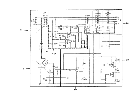
Referring initially to Figure 1 of the drawings, there is
shown a first circuit breaker 10 embodying the invention,
which is for use in a power/load circuit formed a three-
phase mains power supply 11 and a load 12 connected to the
power supply 11 by means of three live power lines R-R', S-
S' and T-T' and a neutral power line N-N'. The circuit
breaker 10 comprises a fault sensor circuit 20 associated
with the power lines R-R', S-S', T-T' and N-N', first and
io second comparator circuits 40 and 50 connected separately
to the fault sensor circuit 20 for fault detection and then
providing a tripping signal, and a tripping circuit 60
connected to the comparator circuits 40 and 50 for breaking
the power/load circuit in response to the tripping signal.
i5 The tripping circuit 60 is formed by a set of four
normally-opened switches SW1 connected in series with the
respective power lines R-R', S-S', T-T' and N-N' facing the
power supply 11, a solenoid SO for normally holding the
switches SW1 closed, and a silicon-controlled rectifier
2o SCR1 connected in parallel with and for disabling (short-
circuiting) the solenoid SO to open the switches SW1 in
order to disconnect the load 12 from the power supply 11.
The tripping circuit 60 includes a full-wave rectifier D
for picking up power from the power nodes R and T to drive
25 the solenoid SO via a micro switch SW2 and to drive the
comparator circuits 40 and 50 via a zener diode D5
CA 02268575 1999-04-06
- 6 -
providing a voltage node vl, said circuits 40, 50 and 60
sharing a common ground E.
The fault sensor circuit 20 is formed by a combined voltage
sensor/comparator 30 connected to the three live power
lines R-R', S-S' and T-T' and by respective current sensing
transformers T1 to T3 each having four primary windings P1
to P4 connected in series along respective power lines R-
R', S-S', T-T' and N-N' at a position downstream of the
switches SW1 and a secondary winding S1. The primary
io windings P1 to P4 of the transformer T1 are balanced for
detecting, by itself, any intolerable earth leakage fault
and, in combination with the voltage sensor/comparator 30,
any intolerable phase voltage imbalance, including phase
failure (missing), in the power/load circuit for action by
i5 the comparator circuit 50.
The primary windings P1 to P4 of the transformer T2 are
made slightly unbalanced by means of resistors R11 and R12
connected in parallel with the primary windings P1 and P4
respectively. The primary windings P1 to P4 of the
2o transformer T3 are made slightly unbalanced by means of
resistors R13 and R14 connected in parallel with the
primary windings P2 and P4 respectively. These two
transformers T2 and T3 are for detecting any intolerable
over-current, including short-circuit fault, in the
25 power/load circuit for action by the comparator circuit 40.
CA 02268575 1999-04-06
The voltage sensor/comparator 30 includes a pair of OP-A~
(operational amplifier) voltage comparators OA1 and OA2 and
a silicon-controlled rectifier SCR2. It has two inputs and
a common node Y connected to respective live power lines R-
R', S-S' and T-T' on the side of the transformers T1 to T3
facing the power supply 11 and an output connected to the
live power line T-T' on the side of the transformers T1 to
T3 facing the load 12. Thus, the voltage sensor/comparator
30 provides a circuit path x extending from the power nodes
io R and S to the power node T' across opposite sides of the
power lines R-R', S-S' and T-T' with respect to and
externally of the transformers T1 to T3.
The two inputs of the voltage sensor/comparator 30 are
provided by respective comparators OA1 and OA2. Each
i5 comparator OA1 (or OA2) has a first input connected to a
respective power node R (or S) by means of a diode-
resistor-capacitor circuit D1-R1-C1 (or D2-R2-C2) across
the power node R (or S) and the remaining power node T
which provides the common node Y. The second input of each
2o comparator OA1 (or OA2) is connected to the first input of
the other comparator OA2 (or OA1) by means of respective
potential dividing resistors R3/R4 (or R5/R6) across the
said first input and the common node Y. Accordingly, the
inputs of the comparators OA1 and OA2 are cross connected
25 the power lines R-R', S-S' and T-T'.
In operation, each comparator OA1 (or OA2) senses a
CA 02268575 1999-04-06
_ g _
respective phase-to-phase voltage R-T (or S-T) of the power
supply 11, with a percentage of the same phase-to-phase
voltage R-T (or S-T) being sensed by the other comparator
OA2 (or OA1). Accordingly, the comparators OA1 and OA2 are
arranged to cross compare one phase-to-phase voltage R-T
(or S-T) with a percentage (the same percentage) of the
other phase-to-phase voltage S-T (or R-T), covering all the
three phases voltages R-S-T. while the three phase
voltages R-S-T are balanced in a healthy condition, the
to voltage differences as sensed by both comparators OA1 and
OA2 are equal and their logic outputs will be the same (at
logic low). In the event of an intolerable phase voltage
imbalance (or a phase failure) in the power/load circuit,
the voltage differences as sensed by the comparators OA1
i5 and OA2 will change in opposite directions, with one
voltage difference increasing while the other voltage
difference decreasing. This will cause the logic output of
one of the comparators OA1 and OA2 and in turn their
combined output to toggle (to logic high).
2o The cross comparison by the comparators OA1 and OA2 between
the two phase-to-phase voltages R-T and S-T is twice as
sensitive compared with the comparison of either phase-to-
phase voltage R-T or S-T against a fixed reference voltage.
The rectifier SCR2 has an anode connected to the power
25 nodes R and S by means of a common resistor R8 and
respective diodes D3 and D4 (also for providing a voltage
CA 02268575 1999-04-06
_ g _
node V2 for driving the comparators OAl and OA2), a cathode
acting as the output of the sensing comparator circuit 30
connected to the power node T', and a gate connected to the
combined output of the comparators OA1 and OA2 for control.
When the combined logic output of comparators OA1 and OA2
toggles to logic high, the rectifier SCR2 will be turned on
and thus connect the two power nodes R and S to the power
node T' via the aforesaid circuit path X externally of the
transformers T1 to T3. This will simulate an earth leakage
io fault in the power/load circuit for the transformer T1 to
detect and the comparator circuit 50 to provide a tripping
signal as described above.
The comparator circuit 40 is formed by an OP-AMP voltage
comparator OA3, an OP-AMP current integrator OA4, and
i5 resistors R43/R44/R45 acting as a potential divider
connected across the voltage node v1 and the ground E . The
comparator OA3 and integrator OA4 have respective first
inputs connected together to a first end of the secondary
windings S1 of the transformers T2 and T3 , second inputs
2o provided with respective reference voltages by means of the
resistors R43/R44/R45, and a combined output connected to
the gate of the rectifier SCR1 of the tripping circuit 60.
The comparator OA3 and integrator OA4 serve to turn on the
rectifier SCR1 in response to the transformers T2 and T3
25 detecting the occurrence of a short-circuit current or an
intolerable overload current in the power/load circuit.
CA 02268575 1999-04-06
- 10 -
The comparator circuit 50 is formed by an OP-AMP voltage
comparator OA5 which has a first input connected to a first
end of the seconding winding S1 of the transformer T1, a
second input provided with a reference voltage by means of
resistors R51/R52 acting as a potential divider connected
across the voltage node V1 and the ground E, and an output
connected to the gate of the rectifier SCR1 of the tripping
circuit 60. The comparator OA5 serves to turn on the
rectifier SCR1 in response to the transformer T1 alone
to detecting the occurrence of any intolerable earth leakage
fault in the power/load circuit or the transformer T1 in
combination with the voltage sensor/comparator 30 detecting
the occurrence of an intolerable phase voltage imbalance or
a phase failure.
The second ends of the secondary windings S1 of all the
transformers T1 to T3 are connected to the ground E.
In the event of a circuit fault, under the control of the
comparator circuits 40 and 50 in conjunction with the
sensor fault circuit 20 as described above, the tripping
2o circuit 60 will disconnect the load 12 from the power
supply 11 through the opening of the switches SW1. The
switches SW1 can only be re-closed manually after the
circuit fault has been cleared. The types of circuit
faults that can be handled by the circuit beaker 10
comprise (1) phase voltage imbalance, (2) phase failure,
(3) short-circuit current, (4) overload current and (5)
CA 02268575 1999-04-06
- 11 -
earth fault leakage current.
Figure 2 shows a second circuit breaker 100 embodying the
invention, which is implemented and operates in a manner
very similar to that of the first circuit breaker 10, with
s equivalent parts designated by the same reference numerals.
The circuit breaker 100 has two major differences.
The first difference lies in the provision of an additional
line O-O' co-extending with the power lines R-R', S-S', T-
T' and N-N' through the transformers T1 to T3, with the
to transformers T1 to T3 including respective fifth primary
windings P5 connected in series along the line O-O'. Also,
the output of the voltage sensor/comparator 30 is connected
to the end O' of the line O-O', instead of the power node
T'.
i5 The second difference lies in the rectifier SCR2 of the
voltage sensor/comparator 30 being connected with its
cathode to the common node Y and its anode acting as the
output of voltage sensor/comparator 30.
The invention has been given by way of example.only, and
2o various other modifications of and/or alterations to the
described embodiments may be made by persons skilled in the
art without departing from the scope of the invention as
specified in the appended claims.