Note: Descriptions are shown in the official language in which they were submitted.
CA 02268595 1999-04-06
1
ENCODER. METHOD THEREOF
AND GRAPHIC PROCESSING APPARATUS
BACKGROUND OF THE INVENTION
1. Field of the Invention
The present invention relates to an encoder
for encoding digital data composed of a plurality of
bits, a method thereof, and a graphic processing
apparatus.
2. Description of the Related Art
Computer graphics are often used in a
variety of computer aided design (CAD) systems and
amusement machines. Especially, along with the recent
advances in image processing techniques, systems using
three-dimensional computer graphics are becoming rapidly
widespread.
In three-dimensional computer graphics, the
color value of each pixel is calculated at the time of
deciding the color of each corresponding pixel. Then,
rendering is performed for writing the calculated value
to an address of a display buffer (frame buffer)
corresponding to the pixel.
One of the rendering methods is polygon
rendering. In this method, a three-dimensional model is
CA 02268595 1999-04-06
2
expressed as an composite of triangular unit graphics
(polygons). By drawing the polygons as units, the colors
of the pixels of the display screen are decided.
In polygon rendering, coordinates (x, y, z),
color data (R, G, B, a), homogeneous coordinates (s, t)
of texture data indicating a composite image pattern,
and a value of the homogeneous term g for the respective
vertexes of the triangle in a physical coordinate system
are input and processing is performed for interpolation
of these values inside the triangle.
Here, the homogeneous term g is, simply
stated, like an expansion or reduction rate. Coordinates
in a UV coordinate system of an actual texture buffer,
namely, texture coordinate data (u, v), are comprised of
the homogeneous coordinates (s, t) divided by the
homogeneous term g to give "s/q" and "t/q" which in turn
are multiplied by texture sizes USIZE and VSIZE,
respectively.
In a three-dimensional computer graphic
system using such polygon rendering, the texture data is
read from the texture buffer when drawing, and texture
mapping is performed for applying the read texture data
on the surface of the three-dimensional model.
The texture mapped image data is written in
a display memory (frame memory) after being subjected to
CA 02268595 1999-04-06
3
predetermined processing.
The above three-dimensional computer graphic
system, however, has a built-in first and second
priority encoder (FSPE) for generating, for example,
positional data of a first "1" bit and a second "1" bit
seen from a most significant bit (MSB) in digital data
comprised of a plurality of bits in a variety of
circuits including for example a division circuit.
Figure 10 is a view of the configuration of
an FSPE encoder 50 of the related art.
As shown in Fig. 10, the FSPE encoder 50
comprises 16-bit priority encoders 51 and 53 and a 16-
bit first valid bit mask unit 52.
In the FSPE encoder 50, input digital data
60 is input to the priority encoder 51 and the first
valid bit mask unit 52.
In the priority encoder 51, a first "1" bit
seen from the MSB in the digital data 60 is detected and
4-bit first bit encode data 61 indicating the position
of the bit is generated.
In the first valid bit mask unit 52, first
valid bit mask data 63, wherein a first "1" bit seen
from the MSB in the digital data 60 is masked, that is,
the bit is changed to "0", is generated and output to
the priority encoder 53.
CA 02268595 1999-04-06
4
Next, in the priority encoder 53, a first
"1". bit seen from the MSB in the first valid bit mask
data 63 is detected and 4-bit second bit encode data 62
indicating the position of the bit is generated.
Below, the processing of each of the
components of the FSPE encoder will be explained in
detail with reference to a flow chart.
[Priority Encoder 51]
Figure 11 is a flow chart of the processing
in the priority encoder 51 in Fig. 10.
Step S1: "0 x Of", that is, a hexadecimal
"Of", is substituted for a variable "sft".
Step S2: The digital data 60 "in" is shifted
toward a least significant bit (LSB) by exactly the
amount of the variable "sft".
Step S3: It is fudged whether or not the
result of the shift at Step S2 is "1".~ When it is "1",
the processing of Step S4 is carried out, while when it
is not "1", the processing at Step S5 is carried out.
Step S4: The value "0 x Of - sft" obtained
by subtracting the variable "sft" from the "0 x Of",
that is, the hexadecimal "Of", is output as the first
bit encode data 61.
Step S5: The variable "sft" is reduced by
"1".
CA 02268595 1999-04-06
Step S6: It is judged whether or not the
variable "sft" is 0 or more. When it is 0 or more, the
processing of Step S2 is carried out, while when not,
the processing of Step S7 is carried out.
5 Step S7: "0 x 00" is output as the first bit
encode data 61.
Note that the processing shown in Fig. 11 is
as shown in Fig. 12 when written in a C language.
The processing in the priority encoder 53 is
the same as that in the above priority encoder 51 except
that the processing is performed on the first valid bit
mask data 63.
[First Valid Bit Mask Unit 52]
Figure 13 is a flow chart of processing in
the first valid bit mask unit 52 in Fig. 10.
Step 511: The value "0 x Of", that is, the
hexadecimal "Of", is substituted for the variable "sft".
Step 512: The digital data 60 "in" is
shifted toward the LSB by exactly the amount of the
variable "sft" .
Step 513: It is judged whether or not the
result of the shift at Step S12 is "1". When it is "1",
the processing of Step S14 is carried out, while when it
is not "1", the processing at Step S16 is carried out.
Step 514: The value "0 x ff", that is, the
CA 02268595 1999-04-06
6
hexadecimal "ff", is shifted toward the LSB by exactly
"0 x 10 - sft" obtained by subtracting the variable
"sft" from "0 x 10". The result of the shift becomes a
"mask".
Step 515: The digital data 60 "in" is
shifted toward the LSB by exactly the amount of the
"mask" obtained at Step 514. The result of the shift is
output to the priority encoder 53 shown in Fig. 10 as
the first valid bit mask data 63.
Step 516: The variable "sft" is reduced by
.,1...
Step S17: It is judged whether or not the
variable "sft" is 0 or more. When it is 0 or more, the
processing of Step S12 is carried out, while when not,
the processing of Step S18 is carried out.
Step S18: The value "0 x 00" is output to
the priority encoder 53 as the first valid bit mask data
63.
Note that the processing shown in Fig. 13 is
as shown as Fig. 14 when written in a C language.
Summarizing the problem to be solved by the
present invention, in the FSPE encoder 50 built in the
above three-dimensional computer graphic system of the
related art, as shown in Fig. 10, two 16-bit priority
encoders 51 and 53 are necessary, so it suffers from a
CA 02268595 1999-04-06
7
disadvantage that the apparatus becomes large in size.
Also, the path on which the first valid bit
mask unit 52 and the priority encoder 53 for performing
the 16-bit operation are placed becomes a critical path
of the calculation processing time, therefore it suffers
from a disadvantage that the processing time becomes
long. There is also a disadvantage that the scale of the
circuit becomes large.
SUMMARY OF THE INVENTION
An object of the present invention is to provide
an encoder, a method thereof, and a graphic processing
apparatus capable of generating positional data of a
first "1" bit and a second "1" bit seen from the MSB at
a high speed with a compact apparatus configuration.
Another object of the present invention is to
provide an encoder and a method thereof capable of
generating positional data of a first "1" bit and a
second "1" bit seen from an LSB at a high speed with a
compact apparatus configuration.
To attain the above objects, according to a first
aspect of the present invention, there is provided an
encoder for detecting a first bit located closest to the
MSB and a second bit located second-closest to the MSB
among bits of a first level included in digital data of n
CA 02268595 1999-04-06
bits (n is an integer not less than 2) and producing
location information of the first bit and the second bit,
comprising a bit number detecting means for detecting the
number of bits of the first level included in an upper nl
bits of the digital data; a first bit location
information producing means for producing first bit
location information which is location information of the
bit located closest to the MSB among bits of first level
included in upper nl bits of the digital data; a first
data masking means for producing digital data in which
the level of the bit located closest to the MSB among
bits of a first level included in upper nl bits of the
digital data is replaced with a second level; second bit
location information producing means for producing second
bit location information which is location information of
the bit located closest to the MSB among bits of a first
level included in lower n2 bits of the digital data; a
second data masking means for producing digital data in
which the level of the bit located closest to the MSB
among bits of a first level included in lower n2 bits of
the digital data is replaced with a second level; a
selecting means for selecting one digital data among the
digital data produced by the first data masking means and
the digital data produced by the second data masking
means on the basis of the detection result of the bit
CA 02268595 1999-04-06
9
number detecting means; a third bit location information
producing means for producing third bit location
information which is location information of the bit
located closest to the MSB among bits of a first level
included in the digital data selected by the selecting
means; and a determining means for determining location
information of the first bit and the second bit by using
the first bit location information, the second bit
location information, and the third bit location
information on the basis of the result of the detection
of the bit number detecting means.
In the encoder according to the first aspect of the
present invention, the upper n/2 bits of the input n-bit
digital data are input to the bit number detecting means,
the first bit positional data generating means, and the
first data masking means and the lower n/2 bits are input
to the second bit positional data generating means and
the second data masking means.
In the above bit number detecting means, the number
of first level bits included in the above upper n/2 bits
of the digital data is detected. Also, in the above first
bit positional data generating means, the positional data
of the first bit is generated, that is, positional data
of a bit positioned the closest to the MSB side among the
bits of the first level included in the above upper n/2
CA 02268595 1999-04-06
bits of the digital data. Also, in the first data masking
means, digital data is generated in which the bit
positioned the closest to the MSB side among the first
level bits included in the above upper n/2 bits of the
5 digital data is rewritten to the second level.
In the second bit positional data generating means,
the second bit positional data is generated, that is, the
positional data of the bit positioned the closest to the
MSB side among the first level bits included in the above
10 lower n/2 bits of the digital data. Also, in the second
data masking means, digital data is generated in which
the bit positioned the closest to the MSB side among the
first level bits included in the above lower n/2 bits of
the digital data is rewritten to the second level.
Next, in the selecting means, one of the digital
data generated by the first data masking means and the
digital data generated by the second data masking means
is selected based on the detection results of the above
bit number detecting means.
Next, in the third bit positional data generating
means, the third bit positional data is generated, that
is, the positional data of the bit positioned the closest
to the MSB side among the first level bits included in
the digital data selected by the selecting means.
Then, in the decision means, positional data of the
CA 02268595 1999-04-06
11
first bit and the second bit are decided from the first
bit positional data, the second bit positional data, and
the third bit positional data based on the detection
result of the bit number detecting means.
Preferably, the selecting means selects the digital
data produced by the first data masking means when the
number of bits of the first level detected by the bit
number detecting means is zero and selects the digital
data produced by the second data masking means when the
number of bits of the first level detected by the bit
number detecting means is not zero.
Preferably, the detecting means uses the second bit
location information as the location information of the
first bit and uses the third bit location information as
the location information of the second bit when the
number of bits of the first level detected by the bit
number detecting means is zero; uses the first bit
location information as the location information of the
first bit and uses the second bit location information as
the location information of the second bit when the
number of bits of the first level detected by the bit
number detecting means is one; and uses the first bit
location information as the location information of the
first bit and uses the third bit location information as
the location information of the second bit when the
CA 02268595 1999-04-06
12
number of bits of the first level detected by the bit
number detecting means is not less than 2.
Preferably, the process of the bit number detecting
means, the process of the first bit location information
producing means, the process of the first data masking
means, the process of the second bit location information
producing means, and the process of the second data
masking means are performed in parallel.
Preferably, the upper nl bits are the upper n/2
bits and the lower n2 bits are the lower n/2 bits.
According to a second aspect of the present
invention, there is provided an encoder for detecting a
first bit located closest to the LSB and a second bit
located second-closest to the LSB among bits of a first
level included in digital data of n bits (n is an integer
not less than 2) and producing location information of
the first bit and the second bit, comprising a bit number
detecting means for detecting the number of bits of the
first level included in an upper n1 bits of the digital
data; a first bit location information producing means
for producing first bit location information which is
location information of the bit located closest to the
LSB among bits of first level included in an upper nl
bits of the digital data; a first data masking means for
producing digital data in which the level of the bit
CA 02268595 1999-04-06
13
located closest to the LSB among bits of a first level
included in upper nl bits of the digital data is replaced
with a second level; a second bit location information
producing means for producing second bit location
information which is location information of the bit
located closest to the LSB among bits of a first level
included in lower n2 bits of the digital data; a second
data masking means for producing digital data in which
the level of the bit located closest to the LSB among
bits of a first level included in lower n2 bits of the
digital data is replaced with a second level; a selecting
means for selecting one digital data among the digital
data produced by the first data masking means and the
digital data produced by the second data masking means on
the basis of the detection result of the bit number
detecting means; a third bit location information
producing means for producing third bit location
information which is location information of the bit
located closest to the LSB among bits of a first level
included in the digital data selected by the selecting
means; and a determining means for determining location
information of the first bit and the second bit by using
the first bit location information, the second bit
location information, and the third bit location
information on the basis of the result of the detection
CA 02268595 1999-04-06
14
of the bit number detecting means.
Preferably, the selecting means selects the digital
data produced by the first data masking means when the
number of bits of the first level detected by the bit
number detecting means is zero and selects the digital
data produced by the second data masking means when the
number of bits of the first level detected by the bit
number detecting means is not zero.
Preferably, the determining means uses the second
10' bit location information as the location information of
the first bit and uses the third bit location information
as the location information of the second bit when the
number of bits of the first level detected by the bit
number detecting means is zero; uses the first bit
location information as the location information of the
first bit and uses the second bit location information as
the location information of the second bit when the
number of bits of the first level detected by the bit
number detecting means is one; and uses the first bit
location information as the location information of the
first bit and uses the third bit location information as
the location information of the second bit when the
number of bits of the first level detected by the bit
number detecting means is not less than 2.
Preferably, the process of the bit number detecting
CA 02268595 1999-04-06
means, the process of the first bit location information
producing means, the process of the first data masking
means, the process of the second bit location information
producing means, and the process of the second data
5 masking means are performed in parallel.
Preferably, the upper nl bits are upper n/2 bits
and the lower n2 bits are lower n/2 bits.
According to a third aspect of the present
invention, there is provided a graphic processing
10 apparatus wherein a three-dimensional model is expressed
by a composite of unit graphics, texture data comprised
of a plurality of pixel data indicating a pattern to be
added to the unit graphics is read from an image memory,
drawing data comprised of a plurality of pixel data is
15 produced by setting the read texture data in
correspondence with the unit graphics, and the drawing
data is stored in the image memory, the~graphic
processing apparatus comprising a polygon rendering data
producing means for producing polygon rendering data
including a three-dimensional coordinates (x,y,z), red
(R), green (G), blue (B) data, homogeneous coordinates
(s, t) and homogeneous term q for the vertexes of the unit
graphics; an interpolation data generating means for
interpolating polygon rendering data of the vertexes of
the unit graphics to generate interpolated data of the
CA 02268595 1999-04-06
16
pixels inside the unit graphics; and a texture processing
means for detecting a first bit located closest to the
MSB and a second bit located second-closest to the MSB
among digital data of n bits (n is an integer not less
than 2), including a division circuit embedding an
encoder producing location information of the first bit
and the second bit, dividing the homogeneous coordinates
(s,t) included in the interpolated data by the
homogeneous term g by using the division circuit, reading
the texture data from the image memory by using texture
address in accordance with the result of the division,
and producing drawing data to be set in correspondence
with the unit graphics, the division circuit comprising a
bit number detecting means for detecting the number of
bits of the first level included in upper nl bits of the
digital data; a first bit location information producing
means for producing first bit location information which
is location information of the bit located closest to the
MSB among bits of a first level included in upper n1 bits
of the digital data; a first data masking means for
producing digital data in which the level of the bit
located closest to the MSB among bits of a first level
included in upper nl bits of the digital data is replaced
with a second level; a second bit location information
producing means for producing second bit location
CA 02268595 1999-04-06
17
information which is location information of the bit
located closest to the MSB among bits of a first level
included in lower n2 bits of the digital data; a second
data masking means for producing digital data in which
the level of the bit located closest to the MSB among
bits of a first level included in lower n2 bits of the
digital data is replaced with a second level; a selecting
means for selecting one digital data among the digital
data produced by the first data masking means and the
digital data produced by the second data masking means on
the basis of the detection result of the bit number
detecting means; a third bit location information
producing means for producing third bit location
information which is location information of the bit
located closest to the MSB among bits of a first level
included in the digital data selected by the selecting
means; and a determining means for determining location
information of the first bit and the second bit by using
the first bit location information, the second bit
location information, and the third bit location
information on the basis of the result of the detection
of the bit number detecting means.
Preferably, the selecting means of the division
circuit selects the digital data produced by the first
data masking means when the number of bits of the first
CA 02268595 1999-04-06
18
level detected by the bit number detecting means is zero
and selects the digital data produced by the second data
masking means when the number of bits of the first level
detected by the bit number detecting means is not zero.
Preferably, the determining means of the division
circuit uses the second bit location information as the
location information of the first bit and uses the third
bit location information as the location information of
the second bit when the number of bits of the first level
detected by the bit number detecting means is zero; uses
the first bit location information as the location
information of the first bit and uses the second bit
location information as the location information of the
second bit when the number of bits of the first level
detected by the bit number detecting means is one; and
uses the first bit location information as the location
information of the first bit and uses the third bit
location information as the location information of the
second bit when the number of bits of the first level
detected by the bit number detecting means is not less
than 2.
Preferably, the process of the bit number detecting
means, the process of the first bit location information
producing means, the process of the first data masking
means, the process of the second bit location information
CA 02268595 1999-04-06
19
producing means, and the process of the second data
masking means are performed in parallel.
Preferably, the upper nl bits are upper n/2 bits
and the lower n2 bits are lower n/2 bits.
According to a fourth aspect of the present
invention, there is provided an encoding method detecting
a first bit located closest to the MSB and a second bit
located second-closest to the MSB among bits of a first
level included in a digital data of n bits (n is an
integer not less than 2) and producing location
information of the first bit and the second bit, the
encoding method comprising the steps of detecting the
number of bits of the first level included in upper nl
bits of the digital data; producing first bit location
information which is location information of the bit
located closest to the MSB among bits of first level
included in upper nl bits of the digital data; producing
first mask digital data in which the level of the bit
located closest to the MSB among bits of a first level
included in upper nl bits of the digital data is replaced
with a second level; producing second bit location
information which is location information of the bit
located closest to the MSB among bits of a first level
included in lower n2 bits of the digital data; producing
a second mask digital data in which the level of the bit
CA 02268595 1999-04-06
located closest to the MSB among bits of a first level
included in lower n2 bits of the digital data is replaced
with a second level; selecting one digital data among the
digital data produced by the first data masking means and
5 the digital data produced by the second data masking
means on the basis of the detected number of bits;
producing third bit location information which is
location information of the bit located closest to the
MSB among bits of a first level included in the selected
10 digital data; and determining location information of the
first bit and the second bit by using the first bit
location information, the second bit location
information, and the third bit location information on
the basis of the detected number of bits.
15 Preferably, the first mask digital data is selected
when the detected number of bits is zero, and the second
mask digital data is selected when the detected number of
bits is not zero.
Preferably, the second bit location information is
20 used as the location information of the first bit and the
third bit location information is used as the location
information of the second bit when the detected number of
bits is zero; the first bit location information is used
as the location information of the first bit and the
second bit location information is used as the location
CA 02268595 1999-04-06
21
information of the second bit when the detected number of
bits is one; and the first bit location information is
used as the location information of the first bit and the
third bit location information is used as the location
information of the second bit when the detected number of
bits of is not less than 2.
Preferably, the process of detecting the bit
number, the process of producing the first bit location
information, the process of producing the first mask
digital data, the process of producing second bit
location information, and the prooess of producing the
second mask digital data are performed in parallel.
Preferably, the upper nl bits are upper n/2 bits
and the lower n2 bits are lower n/2 bits.
According to a fifth aspect of the present
invention, there is provided an encoding method for
detecting a first bit located closest to the LSB and a
second bit located second-closest to the LSB among bits
of a first level included in digital data of n bits (n is
an integer not less than 2) and producing location
information of the first bit and the second bit, the
encoding method comprising the steps of detecting the
number of bits of the first level included in upper nl
bits of the digital data; producing first bit location
information which is location information of the bit
CA 02268595 1999-04-06
22
located closest to the LSB among bits of a first level
included in upper nl.bits of the digital data; producing
first mask digital data in which the level of the bit
located closest to the LSB among bits of a first level
included in upper nl bits of the digital data is replaced
with a second level; producing second bit location
information which is location information of the bit
located closest to the LSB among bits of a first level
included in lower n2 bits of the digital data; producing
second mask digital data in which the level of the bit
located closest to the LSB among bits of a first level
included in lower n2 bits of the digital data is replaced
with a second level; selecting one digital data among the
digital data produced by the first data masking means and
the digital data produced by the second data masking
means on the basis of the detected number of bits;
producing third bit location information which is
location information of the bit located closest to the
LSB among bits of a first level included in the selected
digital data; and determining location information of the
first bit and the second bit by using the first bit
location information, the second bit location
information, and the third bit location information on
the basis of the detected number of bits.
Preferably, the first mask digital data is selected
CA 02268595 1999-04-06
23
when the detected number of bits is zero, and the second
mask digital data is selected when the detected number of
bits is not zero.
Preferably, the second bit location information is
used as the location information of the first bit and the
third bit location information is used as the location
information of the second bit when the detected number of
bits is zero; the first bit location information is used
as the location information of the first bit and the
second bit location information is used as the location
information of the second bit when the detected number of
bits is one; and the first bit location information is
used as the location information of the first bit and the
third bit location information is used as the location
information of the second bit when the detected number of
bits of is not less than 2.
Preferably, the process of detecting the bit
number, the process of producing the first bit location
information, the process of producing the first mask
digital data, the process of producing second bit
location information, and the process of producing the
second mask digital data are performed in parallel.
Preferably, the upper nl bits are the upper n/2
bits and the lower n2 bits are the lower n/2 bits.
CA 02268595 1999-04-06
24
BRIEF DESCRIPTION OF THE DRAWINGS
These and other objects and features of the present
invention will become clearer from the following
description of the preferred embodiments given with
reference to the accompanying drawings, in which:
Fig. 1 is a view of the system configuration of a
three-dimensional computer graphic system according to an
embodiment of the present invention;
Fig. 2 is a view of the configuration of an FSPE
encoder built in the three-dimensional computer graphic
system of the present embodiment;
Fig. 3 is a flow chart of processing in the valid
detector shown in Fig. 2;
Fig. 4 is a flow chart of processing in the valid
detector shown in Fig. 2;
Fig. 5 is a view of an example when the processing
in the valid detector shown in Figs. 3 and 4 is written
in the C language;
Fig. 6 is a flow chart of processing in the
priority encoder in Fig. 2;
Fig. 7 is a view of an example when the processing
in the priority encoder shown in Fig. 6 is written in the
C language;
Fig. 8 is a flow chart of processing in the first
valid bit mask unit shown in Fig. 2;
CA 02268595 1999-04-06
Fig. 9 is a view of an example when the processing
of the first valid bit mask unit shown in Fig. 8-is
written in the C language;
Fig. 10 is a view of the configuration of an FSPE
5 encoder of the related art;
Fig. 11 is a flow chart of processing of the
priority encoder in Fig. 10;
Fig. 12 is a view of an example when the processing
in the priority encoder shown in Fig. 11 is written in
10 the C language;
Fig. 13 is a flow chart of processing in the first
valid bit mask unit shown in Fig. 10; and
Fig. 14 is a view of an example when the processing
in the first valid bit mask unit shown in Fig. 13 is
15 written in the C language.
DESCRIPTION OF THE PREFERRED EMBODIMENTS
Below, preferred embodiments will be described with
reference to the accompanying drawings.
20 Figure 1 is a view of the system configuration of a
three-dimensional computer graphic system 1 of the
present embodiment.
In the three-dimensional computer graphic system 1,
a three-dimensional model is expressed by a composite of
25 triangular unit graphics (polygons). By drawing the
CA 02268595 1999-04-06
26
polygons, this system can decide the color of each pixel
on the display screen and perform polygon rendering for
display on the screen.
In the three-dimensional computer graphic system 1,
a three-dimensional object is expressed by using a z-
coordinate for indicating the depth in addition to the
(x, y) coordinates for indicating positions on a two-
dimensional plane. Any one point of the three dimensional
space can be expressed by the three coordinates (x, y,
z).
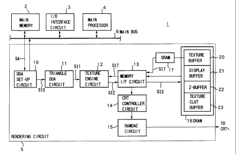
As shown in Fig. 1, in the three-dimensional
computer graphic system 1, a main memory 2, an I/O
interface circuit 3, a main processor 4, and a rendering
circuit 5 are connected via a main bus 6.
Below, the operations of the respective components
will be explained.
The main processor 4, for example, in accordance
with the state of progress in a game, reads the necessary
graphic data from the main memory 2, performs clipping,
lighting, geometrical processing, etc. on the graphic
data and generates polygon rendering data. The main
processor 4 outputs the polygon rendering data S4 to the
rendering circuit 5 via the main bus 6.
The I/O interface 3 receives as input the polygon
rendering data from the outside in accordance with need
CA 02268595 1999-04-06
27
and outputs the same to the rendering circuit 5 via the
main bus 6.
Here, the polygon rendering data includes data of
each of the three vertexes (x, y, z, R, G, B, a, s, t, q,
F) of the polygon.
Here, the (x, y, z) data indicates the three-
dimensional coordinates of a vertex of the polygon, and
(R, G, B) data indicates the luminance values of red,
green, and blue at the three-dimensional coordinates,
respectively.
The data a indicates a coefficient of blending the
R, G, B data of a pixel to be drawn and that of a pixel
already stored in the display buffer 21.
Among the (s, t, q) data, the (s, t) indicates
homogeneous coordinates of a corresponding texture and
the g indicates the homogenous term. Here, the texture
sizes USIZE and VSIZE are respectively multiplied with
the "s/q" and "t/q" to obtain coordinate data (u, v) of
the texture. The texture coordinate data (u, v) is used
for accessing the texture data stored in the texture
buffer 20.
The F data indicates an a value of fogging.
Namely, the polygon rendering data indicates
physical coordinate values of the vertexes of a triangle
and values of colors of the vertexes, texture, and
CA 02268595 1999-04-06
28
fogging.
The rendering circuit 5 will be explained in detail
below.
As shown in Fig. 1, the rendering circuit 5
comprises a digital differential analyzer (DDA) set-up
circuit 10, a triangle DDA circuit 11, a texture engine
circuit 12, a memory interface (I/F) circuit 13, a
cathode ray tube (CRT) controller circuit 14, a random
access memory (RAM) DAC circuit 15, a dynamic random
access memory (DRAM) 16, and a static random access
memory (SRAM) 17.
DRAM 16
The DRAM 16 functions as a texture buffer 20 for
storing the texture data, a display buffer 21 for storing
the display data to be output to the CRT for displaying
on the display, a z-buffer 22 for storing the z-data, and
a texture CLUT buffer 23 for storing the color look-up
data.
DDA Set-up Circuit 10
The DDA set-up circuit 10 performs linear
interpolation of the values of the vertexes of the
triangle on the physical coordinates in a triangle DDA
circuit 11 in its latter part. The DDA set-up circuit 10,
prior to obtaining information of the color and depth of
the respective pixels inside the triangle, performs a
CA 02268595 1999-04-06
29
set-up operation for obtaining the sides of the triangle
and the difference in a horizontal direction for the data
(z, R, G, B, a, s, t, q, F) indicated by the polygon
rendering data S4.
Specifically, this set-up operation uses values of
the starting point, the ending point and the distance
between the two points to calculate the variation of the
value to find movement for a unit length.
The DDA set-up circuit 10 outputs the calculated
variation data S10 to the triangle DDA circuit 11.
Triangle DDA Circuit 11
The triangle DDA circuit 11 uses the variation data
S10 input from the DDA set-up circuit 10 to calculate the
(z, R, G, B, a, s, t, q, F) data after linear
interpolation of each pixel inside the triangle.
The triangle DDA circuit 11 outputs the data (x, y)
for each pixel and the (z, R, G, B, a, s, t, q, F) data
at the (x, y) coordinates to the texture engine circuit
12 as DDA data (interpolation data) 511.
In the present embodiment, the triangle DDA circuit
11 outputs the DDA data S11 of 8 (=2x4) pixels positioned
inside a block being processed in parallel to the texture
engine circuit 12.
Texture Engine Circuit 12
The texture engine circuit 12 performs the
CA 02268595 1999-04-06
calculation of "s/q" and "t/q", calculation of the
texture coordinate data (u, v), reading of the data (R,
G, B, a) from the texture buffer 20, and a blending
successively in a pipeline format.
5 Note that the texture engine circuit 12 performs
the processing on the 8 pixels positioned inside a
predetermined block simultaneously in parallel.
The texture engine circuit 12, by using the
division circuit, performs the operation for dividing the
10 data s by the data g and the operation for dividing the
data t by the data g with respect to the data (s, t, q)
indicated by the DDA data S11. This division circuit
includes a built-in FSPE encoder, which will be explained
later on.
15 Also, the texture engine 12 respectively multiplies
the texture sizes USIZE and VSIZE with the division
results "s/q" and "t/q" to generate the texture
coordinate data (u, v).
The texture engine circuit 12 outputs a reading
20 request including the generated texture coordinate data
(u, v) to the SRAM 17 or the DRAM 16 via the memory I/F
circuit 13. As a result, the texture engine circuit 12
obtains the data S17 (R, G, B, a) stored at the texture
address corresponding to the data (s, t) by reading the
25 texture data stored in the SRAM 17 or in the texture
CA 02268595 1999-04-06
31
buffer 20 via the memory I/F circuit 13.
Here, a copy of the texture data stored in the
texture buffer 20 is stored in the SRAM 17.
The texture engine circuit 12 generates pixel data
S12 by blending the (R, G, B) data in the read data S17
(R, G, B, a) and the (R, G, B) data included in the DDA
data S11 from the triangle DDA circuit 11 in the former
stage by the ratio indicated by the a data (texture a)
included in the data S17 (R, G, B, a).
The texture engine circuit 12 outputs the pixel
data S12 to the memory I/F circuit 13.
Note that in the texture buffer 20, MIPMAP
(textures for a plurality of resolutions) and other
texture data corresponding to a plurality of reducing
rates is stored. Here, which reducing rate of texture
data to use is determined for the above triangular unit
using a predetermined algorithm.
In the case of a full color mode, the texture
engine circuit 12 directly uses the data (R, G, B, a)
read from the texture buffer 20. In the case of an index
color mode, the texture engine circuit 12 reads a color
look-up table (CLUT), prepared in advance, from the
texture CLUT buffer 23, transfers and stores the same in
the built-in SRAM, and uses the color loop-up table to
obtain the data (R, G, B) corresponding to the color
CA 02268595 1999-04-06
32
index read from the texture buffer 20.
Memory I/F Circuit 13
The memory I/F circuit 13 compares the z-data
corresponding to the pixel data S12 input from the
texture engine circuit 12 with the z-data stored in the
z-buffer 22 and judges whether the image drawn by the
input pixel (image) data S12 is positioned closer to the
viewing point than the image written in the display
buffer 21 the previous time. When it is judged that the
image drawn by the input pixel data S12 is positioned
closer, the memory I/F circuit 13 updates the z-data
stored in the buffer 22 by the z-data corresponding to
the pixel data S12 and updates the pixel data in the
display buffer 21 by the pixel data 512.
Also, the memory I/F circuit 13, in accordance with
need, blends the (R, G, B) data included in the image
data S12 and the (R, G, B) data already stored in the
display buffer 21 by the blending ratio indicated by the
a data corresponding to the pixel data 512, that is, a
blending. Then, the memory I/F circuit 13 writes the data
(R, G, B) after blending to the display buffer 21.
CRT Controller Circuit 14
The CRT controller circuit 14 generates an address
for display on a not shown CRT in synchronization with
the given horizontal and vertical synchronization signals
CA 02268595 1999-04-06
33
and outputs a request for reading the display data from
the display buffer 21 to the memory I/F circuit 13. In
response to this request, the memory I/F circuit 13 reads
a certain amount of the display data from the display
buffer 21. The CRT controller 14 has a built-in first in
first out (FIFO) circuit for storing the display data
read from the display buffer 21 and outputs the index
value of RGB to the RAMDAC circuit 15 at certain time
intervals.
RAMDAC Circuit 15
The RAMDAC circuit 15 stores the R, G, B data
corresponding to the respective index values and
transfers the R, G, B data in a digital form
corresponding to the index value of RGB input from the
CRT controller 14 to a digital/analog (D/A) converter to
generate R, G, B data in an analog form. The RAMDAC
circuit 15 outputs the generated R, G, B data to the CRT.
FSPE Encoder
The above three-dimensional computer graphic system
1 has a built-in first and second priority encoder (FSPE)
for outputting the positional data of a first "1" bit and
a second "1" bit seen from the MSB side in digital data
composed of a plurality of bits as an encoding result in
a variety of circuits including the division circuit in
the above texture engine circuit 12.
CA 02268595 1999-04-06
34
Figure 2 is a view of the configuration of the FSPE
encoder 100 of the first embodiment.
As shown in Fig. 2, the FSPE encoder 100 comprises
a valid detector 102, 8-bit priority encoders 103, 105,
and 108, 8-bit first valid bit mask units 104 and 106,
and multiplexers 107, 109, and 110.
Here, the bit number detecting means, the first bit
positional data generating means, the first data masking
means, the second bit positional data generating means,
the second data masking means, the selecting means, and
the third bit positional data generating means of the
' present invention respectively corresponds to the valid
detector 102, the priority encoder 103, the first valid
bit mask unit 104, the priority encoder 105, the first
valid bit mask unit 106, the multiplexes 107, and the
priority encoders 109 and 110. The decision means of the
present invention corresponds to the multiplexers 109 and
110.
The FSPE encoder 100 outputs the positional data of
the first "1" bit seen from the MSB in the digital data
160 as first bit encode data 161 and outputs the
positional data of the second "1" bit as second bit
encode data 162.
[Valid Detector 102]
The valid detector 102 receives as input the upper
CA 02268595 1999-04-06
8 bits of the 16-bit digital data 160, judges whether the
number of "1"s included in the upper 8 bits is 0, 1, or 2
or more, and outputs data "first_vld" and "second_vld"
indicating the result to the multiplexers 109 and 107,
5 respectively.
Specifically, when there is no "1" in the upper 8
bits, "first vld" indicating "0" and "second_vld"
indicating "0" are output to the multiplexers 109 and
107, respectively. When there is one "1" in the upper 8
10 bits, "first_vld" indicating "1" and "second_vld"
indicating "0" are output to the multiplexers 109 and
107, respectively. Also, when there are two or more "1"s
in the upper 8 bits, "first_vld" indicating "1" and
"second_vld" indicating "1" are output to the
15 multiplexers 109 and 107, respectively.
Figures 3 and 4 are flow charts of the processing
in the valid detector 102.
Step S21: The value "0" is substituted for the
variable "count".
20 Step 522: The value "0 x 07", that is, the
hexadecimal "07", is substituted for the variable "sft".
Step S23: "in", that is the upper 8 bits of the
digital data 160, is shifted toward the LSB by exactly
the amount of the variable "sft".
25 Step S24: It is judged whether or not the result of
CA 02268595 1999-04-06
36
the shift at Step S23 is "1". When it is "1", the
processing of Step S25 is carried out, while when it is
not "1", the processing at Step S26 is carried out.
Step S25: The value "1" is added to the variable
"count".
Step S26: The variable "sft" is reduced by "1".
Step 527: It is judged whether or not the variable
"sft" is 0 or more. When it is 0 or more, the processing
of Step S23 is carried out, while when not, the
processing at Step S28 shown in Fig. 4 is carried out.
Step 528: It is judged whether or not the variable
"count" is "0". When it is "0", the processing at Step
S29 is carried out, while when not, the processing at
Step S30 is carried out.
Step 529: This step is performed when the variable
"count" is "0". The "first_vld" indicating "0" and the
"second_vld" indicating "0" are output to the
multiplexers 109 and 107, respectively.
Step 530: It is judged whether or not the variable
"count" is "1". When it is "1", the processing at Step
S31 is carried out, while when not, the processing at
Step S32 is carried out.
Step S31: This step is performed when the variable
"count" is "1". The "first_vld" indicating "1" and the
"second_vld" indicating "0" are output to the
CA 02268595 1999-04-06
37
multiplexers 109 and 107, respectively.
Step S32:. This step is performed when the variable
"count" is 2 or more. The "first_vld" indicating "1" and
the "second_vld" indicating "1" are output to the
multiplexers 109 and 107, respectively.
Note that the processing shown in Figs. 3 and 4 is
as shown in Fig. 5 when written in the C language.
[Priority Encoders 103 and 105]
The priority encoder 103 detects a first "1" bit
seen from the MSB in the upper 8 bits of the digital data
160, generates 3-bit first bit encode data 180 indicating
the position of the bit, and outputs the same to the
multiplexes 109.
Figure 6 is a flow chart of processing in the
priority encoder 103 shown in Fig. 2.
Step 541: The value "0 x 07", that is, the
hexadecimal "07", is substituted for the variable "sft".
Step S42: The upper 8 bits of the digital data 160
"in" are shifted toward the LSB by exactly the amount of
the variable "sft".
Step S43: It is fudged whether or not the result of
the shift at Step S42 is "1". When it is "1", the
processing of Step S44 is carried out, while it is not
"1", the processing at Step S45 is carried out.
Step S44: The value "0 x 07 - sft" obtained by
CA 02268595 1999-04-06
38
subtracting the variable "sft" from "0 x 07", that is,
the hexadecimal "07", is output to the multiplexer 109 as
the first bit encode data 180.
Step S45: The variable "sft" is reduced by "1".
Step S46: It is judged whether or not the variable
"sft" is 0 or more. When it is 0 or more, the processing
of Step S42 is carried out again, while when not, the
processing of Step S47 is carried out.
Step S47: the value "0 x 00" is output to the
multiplexer 109 as the first bit encode data 180.
Note that the above processing shown in Fig. 6 is
as shown in Fig. 7 when written in the C language.
The processing in the priority encoder 105 is the
same as that in the above priority encoder 103 except
that the processing is performed on the lower 8 bits of
the digital data 160 and that the first bit encode data
182 of the processing result is output to the
multiplexers 109 and 110.
(First Valid Bit Mask Units 104 and 106]
The first valid bit mask unit 104 generates first
valid mask data 181 wherein the first "1" bit seen from
the MSB in the upper 8 bits of the digital data 160 is
masked, namely, is rewritten to be "0", and outputs the
same to the multiplexer 107.
Figure 8 is a flow chart of the processing in the
CA 02268595 1999-04-06
39
first valid bit mask unit 104 shown in Fig. 2.
Step S51: The value "0 x 07", that is, the
hexadecimal "07", is substituted for the variable "sft".
Step 552: The upper 8 bits of the digital data 160
"in" are shifted toward the LSB by exactly the amount of
the variable "sft".
Step S53: It is fudged whether or not the result of
the shift at Step S52 is "1". When it is "1", the
processing of Step S54 is carried out, while it is not
"1", the processing at Step S56 is carried out.
Step S54: The value "0 x ff" is shifted toward the
LSB by exactly the amount of "0 x 08 - sft" obtained by
subtracting "sft" from "0 x 08", that is, the hexadecimal
"08". The result of the shift becomes a "mask".
Step 555: A logical product is calculated for the
upper 8 bits of the digital data 160 "in" and the "mask"
calculated at Step 554. The logical product is output to
the multiplexer 107 shown in Fig. 2 as the first valid
bit mask data 181.
Step 556: The variable "sft" is reduced by "1".
Step 557: It is fudged whether or not the variable
"sft" is 0 or more. When it is 0 or more, the processing
of Step S52 is carried out, while when not, the
processing of Step S58 is carried out.
Step 558: The upper 8 bits of the digital data 160
CA 02268595 1999-04-06
"in" are output to the multiplexes 107 as the first valid
bit mask data 181.
Note that the processing shown in Fig. 8 is shown
as in Fig. 9 when written in the C language.
5 The processing in the first valid bit mask unit 106
is the same as that of the above first valid bit mask
unit 104 except that the processing is performed on the
lower 8 bits of the digital data 160 and the processing
result is output to the multiplexes 107 as the first
10 valid bit mask data 183.
[Multiplexes 107]
The multiplexes 107 outputs the first valid bit
mask data 183 from the first valid bit mask unit 106 to
the 8-bit priority encoder 108 as first valid bit mask
15 data 184 when the data seconcLvld is "0". On the other
hand, the multiplexes 107 outputs the first valid bit
data 183 from the first valid bit mask unit 106 to the 8-
bit priority encoder 108 as the first valid bit mask data
184 when the second_vld is "1".
20 [Priority Encoder 108]
The 8-bit priority encoder 108 detects the first
"1" bit seen from the MSB in the first valid bit mask
data 184 from the multiplexes 107, generates 3-bit first
bit encode data 185 indicating the position of the bit,
25 and outputs the same to the multiplexes 110.
CA 02268595 1999-04-06
41
The processing of the 8-bit priority encoder 108 is
basically the same as that of the above priority encoder
103 explained with reference to Figs. 6 and 7.
[Multiplexer 109]
The multiplexer 109 outputs the first bit encode
data 180 as first bit encode data 161 when the data
first_vld is "1", while outputs the first bit encode data
182 as the first bit encode data 161 when the data
first_vld is "0".
[Multiplexer 110]
The multiplexer 110 outputs the first bit encode
data 185 as the second bit encode data 162 when the data
first_vld and the data second_vld are the same values,
while outputs the first bit encode data 182 as the second
bit encode data 162 when the data first_vld and the data
second_vld are different values.
Below, the overall operation of the FSPE encoder
100 shown in Fig. 2 will be explained.
Here, an explanation will be made of the case where
the digital data 160 is "0100000000100000" as an example.
In this case, "01000000", which are the upper bits
of "0100000000100000", are input to the valid detector
102, priority encoder 103, and first valid bit mask unit
104. The lower 8 bits "00100001" are input to the
priority encoder 105 and the first valid bit mask unit
CA 02268595 1999-04-06
42
106.
Next, the processing explained below will be
performed in parallel in the valid detector 102, the
priority encoder 103, and the first valid bit mask unit
104.
Namely, the number of "1"s included in the upper 8
bits is detected to be one in the valid detector 102, and
the "first_vld" indicating "1" and the "second'vld"
indicating "0" are respectively output to the
multiplexers 109 and 107.
Also, the priority encoder 103 detects the first
bit, which is the first "1" bit seen from the MSB (the
MSB is the 0th bit), in the upper 8 bits "01000000" and
outputs the first bit encode data 180 indicating "1" to
the multiplexes 109.
Also, the first valid bit mask data 181 indicating
''0" is output from the first valid bit mask unit 104 to
the multiplexes 107.
In parallel with the above processing on the upper
8 bits, the processing on the lower 8 bits "00100001"
explained below is performed.
Namely, the priority encoder 105 detects the second
bit, that is, the first "1" bit seen from the MSB (the
MSB is the 0th bit), in the lower 8 bits "00100001". The
first bit encode data 182 indicating "2" is output to the
CA 02268595 1999-04-06
43
multiplexers 109 and 110.
In parallel with this, the first valid bit mask
unit 106 outputs the first valid bit mask data 183
indicating "00000001" wherein the second bit of the lower
8 bits "00100001" is masked to the multiplexes 107.
Next, the multiplexes 107, based on the second_vld
indicating "0", outputs the first valid bit mask data 183
indicating "00000001" to the 8-bit priority encoder 108
as the first valid bit mask data 184.
Next, the 8-bit priority encoder 108 encodes the
first valid bit mask data 184 indicating "00000001" and
outputs the first bit encode data 185 indicating "7" to
the multiplexes 110.
Then, based on the first_vld indicating "1", the
first bit encode data 180 indicating "1" is output from
the multiplexes 109 as the first bit encode data 161.
In the multiplexes 110, since the values of the
data first vld and second_vld are different, the first
bit encode data 182 indicating "2" is output as the
second bit encode data 162.
As explained above, according to the FSPE encoder
100 shown in Fig. 2, the 16-bit digital data 160 is
divided into the upper bits and the lower bits and the 8-
bit encode processing and the mask processing are
performed in parallel for both of them.
CA 02268595 1999-04-06
44
In this FSPE encoder 100, the critical path which
determines the processing time is a path of the first
valid bit mask unit 104, the multiplexer 107, the 8-bit
priority encoder 108, and the multiplexer 110.
Here, the respective processing times of the 8 bits
in the first valid bit mask unit 104 and the 8-bit
priority encoder 108 are shorter than the processing of
16 bits in the first valid bit mask unit 52 and the
priority encoder 53 shown in Fig. 10. Furthermore, since
the processing time for switching of the multiplexers 107
and 110 can be ignored, the processing time can be
shorter according to the FSPE encoder 100 shown in Fig. 2
when comparing with the FSPE encoder 50 shown in Fig. 10.
Also, according to the FSPE encoder 100, the
circuit scale aan be reduced comparing with that of the
FSPE encoder 50 of the related art.
The overall operation of the three-dimensional
computer graphic system 1 will be explained below.
Polygon rendering data S4 is output from the main
processor 4 to the DDA set-up circuit 10 via the main bus
6. Difference data S10 indicating the sides of the
triangle and the difference in a horizontal direction
etc. is generated in the DDA set-up circuit 10.
This difference data S10 is output to the triangle
DDA circuit 11. In the triangle DDA circuit 11, the
CA 02268595 1999-04-06
linearly interpolated data (z, R, G, B, a, s, t, q, F)
for each pixel inside the triangle is calculated. Then,
the calculated (z, R, G, B, a, s, t, q, F) data and the
(x, y) data of the vertexes of the triangle are output
5 from the triangle DDA circuit 11 to the texture engine
circuit 12 as DDA data S11.
Next, the texture engine circuit 12 performs the
operation for dividing the data s by the data g and the
operation for dividing the data t by data g for the data
10 (s, t, q) indicated by the DDA data 511.
At this time, the above FSPE encoder 100 shown in
Fig. 2 operates in the division circuit.
Then, the texture sizes USIZE and VSIZE are
respectively multiplied with the division results "s/q"
15 and "t/q" to generate the texture coordinate data (u, v).
Next, a request for reading including the above
generated texture coordinate data (u, v) is output from
the texture engine circuit 12 to the SRAM 17 via the
memory I/F circuit 13. Then, the data S17 (R, G, B, a)
20 stored in the SRAM 17 is read via the memory I/F circuit
13.
Next, in the texture engine circuit 12, the data
(R, G, B) in the read data S17 (R, G, B, a) and the (R,
G, B) data included in the DDA data S11 from the triangle
25 DDA circuit 11 in the former stage are blended by the
CA 02268595 1999-04-06
46
ratio indicated by the a data (texture a) included in the
data S17 (R, G, B, a) to generate the pixel data 512.
This pixel data S12 is output from the texture
engine circuit 12 to the main memory I/F circuit 13.
Then, in the memory I/F circuit 13, the z-data
corresponding to the pixel data input from the texture
engine circuit 12 and the z-data stored in the z-buffer
22 are compared. When the image drawn by the input pixel
data S12 is judged to be positioned closer to the viewing
point than the image drawn in the display buffer the
previous time, the z-data stored in the z-buffer 22 is
updated by the z-data corresponding to the image data
512.
In the memory I/F circuit 13, in accordance with
need, the (R, G, B) data included in the image data S12
and the (R, G, B) data already stored in the display
buffer 21 are blended by the ratio indicated by the a
data corresponding to the pixel data 512. Then the
blended data (R, G, B) is written to the display buffer
21.
The present invention is not limited to the above
embodiments.
For example, 16-bit data was explained as an
example as the digital data 160 shown in Fig. 2 in the
above embodiment, however, the number of bits of the
CA 02268595 1999-04-06
47
digital data 160 is not specifically limited as far as it
satisfies n (nz2). Note that the larger the n is, the
larger the effects becomes.
Also, in the above embodiment, a case of obtaining
the bit position of the first "1" bit and the second "1"
bit seen from the MSB in the digital data 160 was
explained as an example. However, the present invention
can be applied to a case of obtaining the bit positions
of the first "0" bit and the second "0" bit seen from the
MSB in the digital data 160 as well.
Furthermore, the present invention can be applied
to obtain the first "1" bit and the second "1" bit seen
from the LSB and to obtain the first "0" bit and the
second "0" bit seen from the LSB in the digital data 160.
In this case, the lower 8 bits of the digital data
160 are input to the valid bit detector 102, the priority
encoder 103, and the first valid bit mask unit 104 shown
in Fig. 2, and the upper 8 bits of the digital data 160
are input to the priority encoder 105 and the first valid
bit mask unit 106.
Then, at Step S41 shown in Fig. 6, the value "0 x
00" is substituted for the "sft", the "in" is shifted
toward the MSB at Step S42, the shifted result is judged
if it is "10000000" at Step 543, the "sft" is output at
Step S44, the value "1" is added to the "sft" at Step
CA 02268595 1999-04-06
48
545, and the "sft" is judged if it is 7 or less at Step
546.
Also, the value "0 x 00" is substituted for the
"sft" at Step S51 shown in Fig. 8, "in" is shifted toward
the MSB at Step 552, the shifted result is judged if it
is "10000000" or not at Step S53, the value obtained by
shifting "0 x ff" by the amount of the "sft" toward the
MSB is output as "mask" at Step 554, the logical product
of the "in" and the "mask" is output at Step S55, "1" is
added to the "sft" at Step 556, and the "sft" is judged
if it is 7 or less at Step 557.
In the above embodiment, a case where the FSPE
encoder 100 shown in Fig. 2 was built in the division
circuit of the texture engine circuit 12 was explained as
an example. The FSPE encoder 100, however, can be used
when judging to which bank of the display buffer the
texture data read from the texture buffer 20 is to be
written.
For example, in the above explained three-
dimensional computer graphic system 1 shown in Fig. 1,
the configuration using an SRAM 17 was explained as an
example, however, the SRAM 17 may be omitted from the
configuration.
Also, the texture buffer 20 and the texture CLUT
buffer 23 shown in Fig. 1 may be provided outside the
CA 02268595 1999-04-06
49
DRAM 16.
Further, in the three-dimensional computer graphic
system 1 shown in Fig. l, a case where the geometrical
processing for generating the polygon rendering data was
performed in the main processor 4 was explained as an
example, but the processing may be performed in the
rendering circuit 5 as well.
As explained above, according to the encoder and
method of the same and the graphic processing apparatus
of the present invention, the processing time can be made
shorter.
Also, according to the encoder and the graphic
processing apparatus of the present invention, the
apparatus scale can be reduced.
While the invention has been described with
reference to specific embodiment chosen for purpose of
illustration, it should be apparent that numerous
modifications could be made thereto by those skilled in
the art without departing from the basic concept and
scope of the invention.