Note: Descriptions are shown in the official language in which they were submitted.
CA 02268993 1999-04-13
i
Via) TITLE OF THE IPNE~ITION
E1 CONVERTER MODULE rFOR AN ELECTRICAL POWER SUPPLY AND A
SYSTEM INCLUDING IT
(b) TECI-iNIC.~I. FIELD TO WHICH ~ ~N~ON REL.aTES
The present invent'_on relates to a converter modu'_~
designed to supply electrical power both from a =_rst
S source for generating electricity instantaneousl~r, which
source may be a current source, e.g. solar cells, ar_d
from a seccnd source that stores energy, which mav_.be a
voltage scarce, e.q. storace batteries.
(c) BACKGROUND ART
Such converter modules ark intended in particular
for use on-board satellites in order to power a
telecommunicaticns bus. The power Supply system a
controlled from a main control system C~~ which delivers
the signals recuired for operating the various mcdules.
On-board systems generally have three operas==g
ranges, and sometimes only two operating ranges:
I) a~regulation rar_ge or daytime mode: excess power
supplied by the solar cells is diverted or "shunted"
sequeTtially, e.g. using the sc-called" S3R" tec:~.nicue;
II) the battery charging range (BCR)~: excess _cower
delivered by the solar cells is used to charge t'te or
each batter], ar_d the charging current is controlled bv_ a
signal supplied by_the amplifier MEA; and
III) the batter] discharge range (BDR) or "nichttime
mode": currer_t discharge from the batteries is cor_troll~d
by a signal supplied by the amplifier MEA.
When two-range operaticn is used, then range I.
(batter~r charging) is omitted.
A more detailed description of a three-range system
can be found in particular in the publication by
P-R. K. CHETTY, entitled "Improved power conditions~g unit
for regulated bus spacecraft power system", published in
the ESA Proc°edi~gs SP126 of the "3rd ESTEC Spacecraft
Power Seminar", September 21-23, 1977 - NOORDWIJK (pp.
101-110)
In that tec!~.nolegy, each of the operating ranges is
provided by a specific module. For example, the prior
CA 02268993 1999-04-13
art system implements shunt modules
and powered by signals
battery discharge regulator modules
and powered by signals ( and four battery charging
regulator modules and powered by the '
signal
The modules power the line
having capacitance via forward-connected diodes
l0 The modules are powered by the
current generated by the solar cells, while the
modules are powered by the voltage
delivered by the storage battery(ies)
The prior art system is
complicated both from the point of view of the number of
modules and from the point of view of the
interconnections required.
Proposals have already been made to implement both-
way modules~that perform both battery charging II and
discharging III. The resulting saving in~terms of
complexity is relatively marginal, since integrating the
charging function makes it possible to omit only a small
number of modules
Proposals have also been made for a circuit that '
regulates by means of a switched "buck" regulator.
Reference on this topic can be made to the article by
G. SHIVANNA entitled "A new universal spacecraft power
conditioner", published in "ESA Proceedings of 4th
European Research Organization", September 1995, pp. 41
to 45.
(d) DESCRIPTION OF THE IIWENTION '
The idea on which the invention is based is a shunt
type module of topology that makes it possible to adapt a
single module so that it can perform both of the above-
mentioned functions I and III, and preferably to adapt a
single module so that it can perform all three functions
I, II, and III.
CA 02268993 1999-04-13
3
The invention also relates to a converter module for
supplying an electrical power supply from at least a
first source of electricity, in particular a current
source, e.g. a solar panel, the module including a first
branch having self-inductance that extends between a
power supply terminal for the first source and a node
point, and which is functionally associated with a shunt
switch connected between the node point of the first
branch and a common mode pole. It has a second branch '
having in series, between the node point and the common
mode pole: a controlled switch and a filter, in
particular a capacitive filter that is preferably damped.
In particular, the input terminal of the switch can be
connected to an output terminal of the filter and the
output terminal of the switch is connected to said node
point.
The node point is advantageously connected to an
output terminal of the module via a first self-inductive
element. The filter may have a power supply terminal
constituted by an active terminal of a second source of
electrical energy, e.g. one or more batteries. The power
supply terminal of the filter can be'connected to an '
output terminal of an input self-inductive element whose
input terminal is connected to an active terminal of the
second source, where appropriate via a switch element.
The module may have a first or "buck" diode connected in
parallel between the node point and the common mode pole.
In order additionally to give the module a function
of charging the second source, and in a preferred
embodiment, the module includes, in series between the
node point and said active terminal of the second source:
at least one second self-inductive element and at least
one diode that is forward-connected relative to current
for charging such a battery constituting said second
source, and further includes a controllable charging
switch connected between the common mode pole and a
CA 02268993 1999-04-13
terminal common to said diode and to said second self-
inductive element.
The module is advantageously controlled by a control
circuit which presents at least one of the following
S operating modes:
a) the controlled switch can be in its closed
position only if the shunt switch is in its active
position;
b) the controlled switch and the shunt switch are
controlled in phase opposition;
c) the control circuit controls the shunt switch as
a function of the result of comparing the output voltage
from the module and the current flowing through the first
self-inductive element with respective thresholds;
d) the control circuit has a logic element that
deactivates closure of the shunt switch when the control
circuit is in a state of drawing current from or
discharging.the second source; and
e) the~controlled switch is activated on or off in '
response to comparing a sawtooth signal with the output
voltage of the module.
(e) BRIEF DESCRIPTION OF THE DRAWINGS
In the accompanying drawings: '
Figure 1 shows a multi-module system of the prior
art;
Figures 2 and 3 show examples of modules dedicated
respectively to the shunt function and to the discharge
function;
- Figure 4 shows the topology of a shunt module of
the invention;
- Figure 5 shows a control circuit for controlling
the module of Figure 4;
CA 02268993 1999-04-13
- Figure 6 shows an embodiment of a module of the
invention that integrates the shunt and discharge
functions;
~ Figure 7 shows a control circuit for controlling
the Figure 6 circuit;
- Figures 8a to 8d are timing diagrams showing how
the module of Figure 6 operates under certain conditions
under the control of the circuit of Figure 7;
~ Figure 9 shows a multi-module system comprising,
in an embodiment of the invention, modules that combine
the shunt and the discharge functions, or indeed, in a
preferred embodiment, the shunt, the discharge, and the
charging functians, with an example of such a module
being shown in Figure 11; and _
- Figure l0 shows a charging module of conventional
type. y
MORE DETAILED DESCRIPTION
The prior art system shown in Figure 1 implements 32
shunt modules numbered 1 to 32 and powered by the signals S3R,
12 battery discharge regulator modules numbered 1' to 12'
and powered by signals BDR, and four battery charging
regulator modules numbered 1" to 4" and powered by the
signal BCR. -
The modules 1 to_ 32 and 1' to 12' power the line BUS
having capacitance C via forward-connected diodes as
shown.
The modules 1 to 32 and 1" to 4" are powered by the
current SA generated by the solar cells, while the
modules 1' to 12' and 1" to 4" are powered by the voltage
delivered by the storage battery(ies) BAT.
As shown in Figure 1, the prior art system is
complicated both from the point of view of the number of
modules and from the point of view of the
interconnections required.
CA 02268993 1999-04-13
A sequential switching shunt regulation module or
"S3R" module is shown in Figure 2. Starting from an
active terminal A at which current appears from an array '
of solar cells having stray capacitance Cp and delivering
a current Is, and going to an output terminal B, this
module presents in series: a forward-connected diode D;
an inductor Lp whose inductance can be less than 10 uH,
for example (e. g. a few ~.H); and two forward-connected
Schottky diodes D1 and D2, e.g. of the 60HQ100 type which
produce a total voltage drop of about 1.1 V. The output
terminal B is connected to the power supply bus BUS which
has capacitance C. The following are connected in
parallel between the terminal E which is common to the
inductor Lp and to the diode D1, and the common mode pole
(or ground)
CA 02268993 1999-04-13
6
- firstly a controllable shunt switch SS in series
with a calibrated resistor Rs for limiting current in
shunt operations and
- a diode D3 in parallel with a resistor R3 and
connected in series with a capacitor C3 to form a damping
circuit avoiding voltage surges which, when the shunt
switch SS is opened, would otherwise be generated by the
residual inductance between the shunt switch SS and the
capacitance C of the bus BUS.
The solar panels are arranged in sections CS. In
operation, certain sections are associated with modules
whose shunt switches SS are open, powering the bus BUS,
in other sections the modules are shunted, and in one
section there are one or more modules which are switched
sequentially, being alternately in circuit and shunted,
so as to regulate the voltage on the bus BUS.
The shunt switches SS are controlled in on/off mode.
The efficiency of this shunt regulator is of the
order of 97.5. In sections that are shunted, the notion
of efficiency is of no importance since the power
concerned is in excess and must be dissipated. For
sections which are permanently shunted, dissipation is
generally not high.
In contrast, for the modules of the shunt section
that is under sequential control, dissipation is critical
since the stray capacitance Cp of the array of solar
cells discharges completely through the inductor Lp each
time the shunt switch SS closes, thereby generating
losses which fortunately are at the low frequency at
which the shunt is switched. For a solar array
delivering 7 A at a voltage of 50 V, the stray
capacitance Cp is of microfarad order and losses are of
the order of 10 W to 15 W for the corresponding section.
The module shown in Figure 3 is a battery discharge
regulator.
The embodiment shown is appropriate to the case
where battery voltage is greater than that of the bus
CA 02268993 1999-04-13
7
BUS, but it is well known how to modify this topology so
as to include therein a voltage-raising module so as to
form a boost regulator.
The function of the discharge regulator is to
control the current delivered by the battery(ies) to the
bus BUS.
For a battery voltage that is higher than the bus
voltage, the best configuration is the series regulator
("buck converter" -see the above-mentioned article by
G. SHIVANNA). This circuit comprises, between the input
terminal G and the output terminal B connected to the'bus
BUS: a protection switch Sbat, an input inductor L~, a
series regulation switch (~~buck«_switch) S1, an output
inductor Lout, and a forward-connected diode D3. An input
filter, e.g. a damped input filter, comprises, in
parallel between. the terminal H and the common mode pole:
a capacitor C1 in parallel with a capacitor C~1 and damped
by a resistor R~1. These modules are designed to be
connected in parallel to form a corresponding number of
controlled current sources. In addition;~.a "buck' diode
is reverse-connected between the point J-common to S1 and
Lout and the common mode pole M. -
(~ ~T LE.~ST ONE i~iODE FOR CARRYING OUT THE INVENTION
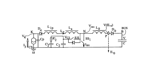
Figure 4 shows._the module of the invention whose
topology enables the shunt function to be performed. The
module as shown in Figure 4 performs the shunt function
only, however, as explained below, it can be adapted to
perform both the above-mentioned shunt function and the
above-mentioned discharge function.
It comprises in succession, between the terminal K
connected to one of the terminals of an array of solar
cells (current Is, stray capacitance Cp) and the terminal
B connected to the bus BUS: a forward-connected diode D4,
an inductor Llp, an inductor Lg, an output inductor Lo,
and an output diode Do. D4, Llp, and Ls constitute a first
branch extending between the point K and the node point
I~. Between the node point N common to the two inductors
L~ and Lo, and the common mode pole, there are connected
CA 02268993 1999-04-13
8
firstly a controlled switch Sli in series with a
preferably-damped filter C'a, R'2, Ca, with that assembly
constituting a second branch. There is also a shunt
switch SSi connected between the node point N and ground.
Lo and Do constitute an output branch.
The components Lo, 51~, Cz, R' 2, and C' 2 are analogous
to the components Lout, S1, Cl, R ~ l, C ~ 1 of Figure 3 . Ls, a
low inductance inductor ~ 10 ~cH) is used to control
the shunt current instead of using a resistive current
limiter in series with the controlled switch SS as shown
in Figure 2. This makes it possible to limit losses:in '
the shunt switch Sl.
The damping circuit (C2, R'z,_ C'2) which is put into
circuit and taken out of circuit b~y the switch S11 serves
I5 advantageously to limit voltage surges when opening the
switch SS1. In its most general form, the filter can be
of any type,,in particular it can be capacitive, suitable
for reducing, voltage surge when the switch SS1 is opened.
To this end, it is advantageous to ensure that the switch
S1z cannot be in the closed position unless the switch SS1
is in the open position. Preferably, S11'is in the open
state when SS= is closed, and S11 is Closed when SSi is in
the open state.
The above-described damper circuit serves
simultaneously to protect the shunt module against
voltage surges and to filter a battery discharge
regulator, thus making the above-mentioned adaptation
possible.
The circuit can thus be adapted as a module that
performs two functions (shunt regulator for solar cells
and discharge regulator for batteries).
Unlike the prior art shunt which requires two diodes
connected to the bus (D1 and D2, Figure 2), the shunt of
the invention requires cnly one (Do, Figure 4) for the
following reason.
In the event of a fault in the short circuit diode,
the capacitance of the bus (C in Figure 2 or Figure 4) is
CA 02268993 1999-04-13
9
connected to the bus via the inductor Lo. By controlling
the current flowing through the inductor using a limit
cycle system, the mean current flowing through the
inductor naturally settles around zero if the shunt
switch SS1, Figure 4, is actuated by the regulation
(signal MEA). It thus suffices for the current sensor in
Lo to be capable of measuring a current around zero in
order to obtain this effect naturally, and this applies
in particular to a Hall effect current sensor.
In the event of a short circuit fault in the diode
Do, the solar panel section (Is, Cs) delivers all its
current if the shunt switch SS1 is not controlled by the
regulation effect, or else a mean current around zero
having a peak-to-peak value that corresponds to the
hysteresis of the limit cycle. In the event of the
entire module operating as a battery discharges (Figure
6), this fault does not affect operation either.
The topology of Figure 4 is associated with a
control circuit as shown in Figure 5, suitable for taking
account of the output inductor Lo.
In the topology of Figure 2, the output impedance of
a solar cell section as seen by the bus BUS is close to
zero, and as a result the capacitance C of the bus BUS is
charged directly by the current produced by the solar
cell section, thereby giving rise to a linear increase in
the voltage V on the bus. When this voltage reaches the
upper threshold of a hysteresis comparator, the shunt
switch SS1 is closed, thereby giving rise to a deficit of
current on the bus and to a decrease in the voltage v
until the lower threshold of the hysteresis comparator is
reached, thereby causing the shunt switch SS1 to be opened
again.
With the module of Figure 4, the output inductor Lo
has the effect that the current produced by the solar
cell section is not directly available on the bus as soon
as the shunt switch SS1 is opened. The current is
established at a rate that is determined by the
CA 02268993 1999-04-13
1V '
difference between the voltage on C2 and the voltage V
across the terminals of C.
If the function of Ls is ignored, where Lg serves
only to control peak current in shunt mode, the problem
seen from CZ is the same as in Figure 2. Cz can be taken
to the open circuit voltage of the solar cell section
which is higher than the operating voltage when operating
at full power.
Figure 5 shows the control circuit associated with
the module of Figure 4. The additional elements (R1~,
INV.1) compared with a conventional control circuit for
the shunt module of Figure 2 are drawn in heavy lines.
As can be seen in Figure 5,-the voltage V so the bus
divided by a bridge R1~/R11 is compared with the voltage of
a zener diode Zl. This comparison is performed at the
inputs of an operational amplifier MEA. The output from
MEA is fed to the inverting input of the comparator COMP1
via a resistor R15. At that point it has added thereto
the voltage V (ILo) from the point P common the inductor
Lo and the forward-connected diode Do, via the resistor
R1~. The reference voltage V of the shunt is applied to
the non-inverting input of COMP1 via'a resistor R14.
Since the resistor R16 is connected to provide positive
feedback, the amplifier COMP1 operates in on/off mode to
control the shunt switch SS1, and via a logic inverter
INV1 to control the switch Sli.
As a result, the switches SS1 and S11 are operated in
phase opposition.
The measure of the current ILo inserter via the
resistor R1., modifies the comparison performed by the
hysteresis comparator and creates a current cycle of
limited amplitude about a given point, thereby giving
rise to more stable operation of the Figure 4 shunt, and
thus reducing voltage ripple on the bus.
It will be understood that if compensation by means
of the current ILo is not implemented, then operation '
CA 02268993 1999-04-13
Ll
continues to be possible but the delaying effect of Lo '
makes performance less satisfactory.
Controlling S11 makes it possible to connect Ca to
the bus when the shunt switch SS1 opens. If the module is
used solely as a shunt, then R'2 and C'2 can be omitted,
with the filter being reduced to a single capacitor C
The operation of the Figure 4 shunt module as
controlled by the circuit of Figure 5 is described in
greater detail below.
For a given load on the bus, and if the array of
solar cells presents No sections, then n sections are
directly coupled to a bus, No-n-1 sections are shunted
(their switches SS1 are closed),_and one section serves to
regulate the voltage on the bus by being controlled
sequentially to act as a shunt. It is the operation for
regulation purposes of this section that is described
below.
The presence of the inductor L$ e.g. of inductance
10 ~H, makes it possible to limit the peak current to
15.8 A for an array of solar cells delivering 50 V and
having stray capacitance of 1 ~F.
It is assumed that the system i~ in a state where
the solar cell section is fully shunted and the output
current through Lo is zero.
The current deficit on the bus causes the voltage on
the bus to decrease and the output from the amplifier MEA
(Figure 5) drifts in the negative direction until the
threshold of the comparator COMP1 is reached.
The shunt switch SS1 is then opened and S11 is
closed. The capacitor Ca, which was previously isolated
by S11, has retained a voltage close to that of the
voltage V on the bus or the voltage V' on the solar
array.
When the switch SS1 is opened, the current I$
delivered by the solar cells begins to charge the stray
capacitance in the vicinity of the voltage VS$ of the
solar array section. Before this voltage is reached, the
CA 02268993 1999-04-13
1~
voltage of the solar array exceeds the voltage V of the
bus or the voltage across the terminals of C1, and current
begins to flow through Lo.
This gives rise to two effects. Firstly there
exists a point where sufficient current is delivered to
the bus to transform the voltage drift from the negative
direction to drift in the positive direction. The second
effect is that simultaneously a positive voltage
resulting from the current through Lo appears at the input
of the comparator COMP1, thereby leading to drift in the
value of the voltage which the bus needs to reach in
order to cause the shunt switch SS1 to be closed again.
When SS1 is closed again, two possible cases exist.
In the first case ("continuous conduction"), the voltage
V on the bus reaches the lower threshold before the
current has ceased to pass through Lo.
In the second case ("discontinuous conduction"), the
current has completely stopped flowing through Lo before V
reaches the lower threshold. In both modes, the maximum
amplitude of current excursion through Lo is substantially
the same and it is determined by the hysteresis of the
comparator COMP1. -
Figure 8a gives voltage and current timing diagrams
at the main points of the circuit in "continuous
conduction" (current in the inductor not interrupted),
' and Figure 8b gives the same timing diagrams for
"discontinuous conduction" (current through the inductor
interrupted).
On the voltage V, ripple remains below 200 mV in
both cases (V = 50 V).
The voltage VCa across the terminals of CZ increases
slightly when the shunt is closed in high current mode,
because of the energy accumulated in Lg.
The amplitude of ILo in both modes is fixed by the
switching hysteresis cycle.
The value of Issl in both modes corresponds to
discharging CP through L$ .
CA 02268993 1999-04-13
1.3
The shunt of Figure 4 does not present switching
losses since, when SS1 is closed, the current through Lo
is subtracted from a current of exactly the same
magnitude delivered by Ls, which means that only a
resonant discharge current of the stray capacitance CP of
the solar array through Ls is seen by SS1 in the closed
state and by the shunted section.
Operating stability is provided by the following
elements:
~ current cycle of limited amplitude; and
no oscillation or drift in voltage or current is
possible at an undesired frequency.
Operating frequency is determined by the hysteresis
of the comparator COMP1, whence the limited current cycle
and the moderate value of the ripple in the bus voltage
V.
Figure 8c is a graph in which the curve representing
the current ISO as a function of the voltage V$ of the
array of solar cells is shown at the opening of the shunt
switch SSl.
Portion I corresponds to charging Cp. 1'nlhen the bus
voltage V is reached, Cp continues t~ be charged, the
voltage continues to rise, but the current decreases
(portion II of the curve). The current I begins to be
established through Lo, and the current supplied ends up
by rising (portion III of the curve) to the point where
the maximum power Pmax is delivered.
In the event of a sudden transient taking current
from the bus, it might nevertheless be feared that there
would be an abnormal voltage drop on the bus. However
this does not happen since the voltage of the solar array
can rise sufficiently to force current through Lo.
Figure 6 shaws a module associating a shunt function
and a battery discharge function. Elements common with
the module of Figure 4 are given the same references.
The additional elements are the battery Bat, the safety
switch Sbat, the inductor Lin and the diode DB. The node
CA 02268993 1999-04-13
1 'f
point N is very important since that is where summing
takes place between the currents supplied by the solar
cells and the currents supplied by the battery(ies).
In its most general form, the filter is then of the
damped capacitive type so as to satisfy simultaneously
conditions relating to discharge mode (filtering) and to
shunt mode (protection against voltage surges).
It will be observed that in battery discharge mode
(S11 closed), the shunt switch SS1 is kept open to allow
the two above-mentioned currents to be added together, in
particular in electrical propulsion mode where the
current through Lo can be greater than the current which
the solar panels can supply.
When S11 is closed, it is nevertheless possible to
use the shunt switch SSl to increase the efficiency of the
system in discharge mode, but in that case, use of the
current supplied by the solar cells is not optimized.
Figure 7 shows a control circuit suitable for the
module of Figure 6. The portion which is situated in the
dashed-line box corresponds to operation~in shunt mode as
shown in Figure 5.
The output from the amplifier MBA is also applied
via a resistor R2o to the inverting input of an
operational amplifier AMP which has a negative feedback
resistor Ra2.
The outputs from the comparators COMP1 and AMP are '
applied to the inverting input of a comparator COMP2
having a resistor R23 mounted to provide positive feedback
and having its non-inverting input receiving a sawtooth
voltage PWM. The output of COMP2 is applied to S1 via a
logic inverter INV1, but the switch SS1 is controlled by
an AND gate having one input receiving the output from
the comparator COMP2. The other input of the AND gate
receives the output from an inverter INV2 whose input is
connected to the output of a comparator amplifier COMP2
having a resistor R25 connected to provide positive
feedback, having its non-inverting input connected to the
CA 02268993 1999-04-13
output of the comparator MEA and having its inverting '
input connected to receive a reference voltage Vref(BDR)
which determines the battery discharge operating range.
The function of the comparator COMP3 is to determine
5 whether the system is in the shunt mode operating range
or in the discharge mode operating range.
If the output signal from MEA is such that the
system is in discharge mode, the output from the
comparator COMP3 causes the switch Sbat to close and the
10 shunt switch SSl is deactivated via the inverter INV2
which produces a logic zero at its output, thereby
turning off the AND gate.
The reference value of the current amplifier AMP is
determined by the output from the amplifier MEA which
15 gives a signal proportional to the voltage error on the
bus relative to the reference set by the zener diode Z1.
The output from the current amplifier AMP is compared '
with the sawtooth signal PWM to control the switch S11 via
the output from comparator COMP2.
The output of COMP2 is also applied~to the other '
input of the AND gate to control the shunt switch SS1 when
closure thereof is not deactivated by closure of the
switch Sbat. It will be observed that the current
controlling the shunt switch SS1 also passes through the
comparator COMP2, but its operation is not affected by
the presence of the sawtooth signal since it operates at
a lower frequency, thus providing a filter effect, and
the signal controlling the shunt switch SS1 is in a logic
state 1 or a logic state 0 which is not modified by the
existence of the sawtooth signal.
The switch Sbat can also operate to protect in
conventional. manner the module in the event of a voltage
surge, by means of a logic circuit which is not described
herein. Sbat can also be taken out of circuit in the
event of a failure of the diode, the shunt switch SS1, or
indeed in the event of the current sensor drifting.
CA 02268993 1999-04-13
1b
The module of the invention can be integrated to a
great extent, as shown for example by the topology of
Figure 9 which makes use of 20 modules M1 to M20 each
powered by the solar array in one or more sections, by
the battery(ies) BAT in one or more sections, and by the
control signals delivered by the control circuit CMEA.
In the two function case (shunt and discharge), the
modules may, for example, be as described in Figure 6,
and they can be controlled individually or in sections,
as described with reference to Figure 7.
Alternatively, the modules can also be adapted.to be
capable of performing the battery charging function, e.g.
by adding an additional charge regulating circuit to some
of the modules and as shown in Figure 10. In principle,
a charge regulator is used conventionally for each
battery. The circuit shown in Figure 10 has a switch Slo,
two reverse-connected diodes, a series inductor Llo, and
two forward-connected diodes (D11, Dia) in series between a
terminal of a voltage boosting circuit SB and the active
terminal of the battery Bat to be recharged.
This circuit is nevertheless not optimum, since
recharging is powered by the bus and'the power delivered
on the bus is reduced by the efficiency coefficient of
the shunt.
A preferred embodiment consists in integrating the
charging regulator in the corresponding module, using the '
circuit shown in Figure 11 in which elements in common
with Figure 6 retain the same references. In this
topology, the current supplied by the solar cells is used
directly to charge the batteries in charging mode.
The additional elements of Figure 11 are the
inductor L'lo connected between the node point N and the
point T, two forward-connected diodes D14 and D15 between
the point T and the active terminal of the battery Bat,
and the voltage boost switching circuit SB1 for forming a
voltage boost regulator.
CA 02268993 1999-04-13
1/
In the charging position, Sbat is open, SS1 is open,
and S11 is closed so that the current I$ is fed both to
L' la and to Lo.
It will be observed that in the event of SB1 failing
in the closed state, this amounts to the module remaining
permanently shunted and the fault does not propagate to
the other modules.
The advantages of the topology of the module of the
invention are summarized below:
~ low shunt switching losses because of _the
presence, by compensation, of zero current during
shunting;
- small ripple in the voltage V on the bus in a
stable operating state;
~ higher operating frequency than in the prior art;
and
~ it is possible to use a single Schottky diode in
the output instead of using two as before (see Figure 2).