Note: Descriptions are shown in the official language in which they were submitted.
CA 02269212 1999-04-19
METHOD FOR VVI~F~ S INFORMATION TRANSFER
Description
s
The invention relates to a method as in claim 1, as well as to a
tr2n~milter and receiver arrangement for implementation of the method
as in claim 12.
10 In wireless information transfer methods, that are well known to the
expert from standard reference works, the information signal to be
transmitted is modulated upon a high frequency carrier signal in the
tr~n.~milter and transferred over a transmission path to the receiver,
which contains a corresponding demodulator for the recovery of the
15 information signal. A well known modulation method in
telecommunications is the angle modulation (as generic term for
frequency and phase modulation).
If the information signal to be tr~n.~mitte-l is present in digital form as a
20 bit sequence, as is the case in modern mobile radio networks, then the
modulation is carried out by variation of the frequency, or phase, or
amplitude of the carrier signal, depending on the bit sequence to be
transmi~te~l. Various digital modulation method~s are known, for example
from COUCH, L.W.: Digital and Analog Communication Systems, 4th
25 Edition, Macmillan Publishing Company (1993), among them amplitude-
shift keying (ASK: Amplitude Shift Keying), two phase-shift keying (2-
PSK: Phase Shift Keying) or two frequency-shift keying (2-FSK:
Frequency Shift Keying). Here too a demodulation is carried out in the
receiver according to the modulation method employed on the transmitter
CA 02269212 1999-04-19
side, thus effecting a recovery of the digital info~mation signal as a bit
sequence in form of consecutive pulses.
The use of several difrerelll modulation methods for dirrerelll messages,
S or message components, as part of a continuous transmission process is
known to the expert, for example from analogue television engineering,
where the vestigial side-band amplitude modulation is used for the
lllmin~nce signal, the frequency modulation for the audio signal, and the
IQ modulation for the chromin~nce signal. Here too, the variation of the
10 carrier parameters serves only in the imprinting of the information and
has no effect on noise of the tr~n.~mi.csion path.
A method for expansion of emitted tracking pulses on the transmitter side
and compression on the receiver side is known from radar technology
lS (~Chirp~-technique); compare E. Philippow (Publisher.): Taschenbuch
der Elektrotechnik,-Vol. 4, Systeme der Informationstechnik, Berlin
1985, p. 340,341. Hereby an analogue frequency modulation or a digital
phase modulation is applied in the compression, but no imprinting of
information takes place. This method serves in the reduction of the
20 expended tr~n~mi~sion power, and thus a potential opponent's ability to
detect the signals, while siml-lt~neously m~int~inin~ range and accuracy
of coverage.
A basic physical problem exists in all communication methods: the
25 quality of the information signal that is recovered on the receiver side
decreases with the amount of intelÇerellce on the transmission path
(always present in reality), and thus with the distance between transmitter
CA 02269212 1999-04-19
and receiver. To obtain a desired working distance at a predetermined
noise immllnity in a co.~ ication over a noisy tr~n.~mi~sion path, a
certain transmission power is n~ce~s~ry, which, for example for mobile
comml-nications, is in the range of Watts.
On one hand, the required ~ power has the disadvantage that the energy
co~ lion during the tr~ncmittin~ operation is correspondingly high, which in
particular for battery or ~ccum~ tQr battery operated devices, such as mobile
telephones, is a problem, due to the rapid depletion of the energy store. On theother hand, the rising number of co.. ~ ication tr~ncmitSers caused by the
explosive distribution of mobile telephones, the increasing number of providers of
radio broa~lcactc and television programs etc, increases the total impact of
electrom~n~tic radiation on hllm~n.c (so called "human exposure"). Harm to the
human body can not be ruled out, in particular for mobile telephones at the
15 presently customary tr~ncmitter power, due to the very low ~ict~n~e of the
trancmitter to the user's head.
This invention has the objective to develop a method of the type
mentioned at the beginning, and an arrangement for the implementation
20 thereof, which allows a reduction in transmission power and/or and
increase in range while m~int~inin~ at least equal tr~n.~mi~sion quality.
This objective is met, starting with a method according to claim 1, by
this method's characterizing features, and - regarding the arrangement
25 for implementing the method - by the features of claim 12.
The invention includes the principal thought to use two independent
modulation methods to imprint the information ont~ a carrier (information
signal modulation) and to achieve extensive suppression of noise on the
CA 02269212 1999-04-19
tr~n.emi~sion path, in particular of the thermal or ~white" noise (carrier
signal modulation).
The pulses that have been mod~ ted, or are to be mod~ ted, with the
5 information according to a well known method of teleco~ ications,
in the tr~n.~mitter are subjected to an angle modulation (which here is to
be understood as generic term for phase and frequency modulation) with
a special characteristic. The angle mod~ ted pulses, showing a
predetermined frequency spectrum, are time compressed in the receiver
10 by introducing a frequency dependent delay. Thus an amplitude
enhancement results at the receiver output, compared to the amplitude of
the tr~n~mitte-l signal, and thus to the noise level. In particular, this
pulse compression / amplitude enhancement can be carried out using a
dispersive filter. The information signal is recovered from the carrier
15 processe~l in this manner by demodulation, whereby the demodulation of
the information signal occurs with a signal/noise ratio improved by the
amplitude enhancement.
The improvement of the signal/noise ratio is dependent on the bandwidth-
20 time-product of the bandwidth used in the angle modulation and the pulse
duration, and is especially prominent in poor tr~n~mi~sion conditions.
The actual information can be imprinted onto the carrier by pulse
modulation techniques, or by carrying out the carrier compression so that
25 it can be evaluated in dirrelent ways for different states of the
information signal, so that the information is contained in this variation
of the angle modulation. Hereby it is important that the modulation of
CA 02269212 1999-04-19
the infolmation has no, or only secondary, influence on the signal delay
time.
After the demodulation the available signal is of a quality, which in the
S state of technology could only be achieved by increased transmitting
power or by costly methods for the improvement of reception (such as
diversity reception or re~ n~l~nt tr~ncmi~sion). A further advantage of
this invention's method lies in the essentially lower potential for
interference compared to other transmission paths, because a
10 predetermined signal/noise ratio can be achieved after the pulse
compression in the receiver using lower transmitting power. In addition,
the lower demands on the transmitting power lead to a reduced human
exposure. The disadvantage of this method, a higher required bandwidth,
and thus a reduced channel capacity or transfer rate (bit rate) can be
15 accepted for many areas of application, and can be partially elimin~ted
through the selection of a matching pulse modulation method for the
modulation of the i~fo~ ation (see below).
A special angle modulation time characteristic is used in the variable
20 angle modulation, which corresponds to a "modulation characteristic
curve". Hereby, the modulation characteristic curve - here referred to as
modulation characteristic - determines the time behavior of the frequency
during the duration of each pulse. When a linearly falling modulation
characteristic is used, the frequency of the transmitted signal decreases
25 linearly, during the duration of each pulse, from a value above the carrier
frequency to one lying below the carrier frequency. Analogously, a
linearly rising characteristic can be used. The filter on the receiver side
CA 02269212 1999-04-19
is matched to the employed modulation characteristic by a corresponding
dirrerenlial, freq~ency dependent delay time response (group delay
response) in such a way that the signal components of different phase
position, generated on the transmitter side are superimposed to a signal
5 nearly coincident in time (approximate ~-pulse).
In an advantageous embodiment of the invention the imprinting of the
information of the input signal occurs by selecting or varying the
modulation characteristic depending on the input signal. If the input
10 signal contains a high-level, then, for example, a modulation
characteristic decreasing (most simply linearly) with the signal is used,
which leads to a frequency modulated pulse with a frequency decreasing
during the pulse duration ("Down-Chirp"). In contrast, a (linearly) rising
modulation characteristic is used for a low-level of the input signal,
15 which correspondingly yields a pulse with a frequency that rises during
the pulse duration (~Up-Chirp").
The filter means on the receiver side are matched by an inverse or
complementary characteristic. If the angle modulation on the transmitter
20 side is carried out according to a decreasing modulation characteristic,
then the frequency of the pulse decreases during the pulse duration,
which has as a result that the signal components of higher frequency
arrive on the receiver side before the signal components of lower
frequency. Thus, the delay time response of the dispersion filter on the
25 receiver side has to compensate for the ~lead" of the high frequency
signal components, so that the spectral signal components of the
.,
CA 02269212 1999-04-19
frequency mo~ te~1 pulse superpose to form a pulse with increased
amplitude at the output of the dispersion filter.
To tr~n~mit a higher information content with each pulse, it is possible
S to use more than two modulation characteristics for the input signal. If,
for example, four modulation characteristics are available, then
accordingly four dirreLenl pulses can be tr~n~mitted, which corresponds
to an infollllation content of 2 bit for each tr~n~mitted pulse. By
increasing the number of different modulation characteristics, the data
10 transfer rate can be advantageously increased, whereby it must be noted
that the technical expense increases at the same time, and the different
pulses with a very large number of different modulation characteristics
become more difficult to distinguish, which increases the transmission's
susceptibility to errors.
In the previously described variation of the invention, the modulation of
pulses is carried out actively for a high-level as well as for a low-level
of the digital input signal. This means that frequency modulated pulses
are generated for a high-level as well as for a low-level of the input
20 signal, which can be distinguished by the type of frequency variation
during the pulse duration. Hereby, the imprinting of the information
contained in the input signal occurs through selection or variation of a
modulation characteristic, depending on the input signal.
25 Alternatively, the transmission of the input signal can be carried out
actively for only one of two defined levels, while no pulse is generated
for the other level. For example, a linearly rising frequency modulated
CA 02269212 1999-04-19
pulse is generated for a high-level of the input signal, while a pause of
the pulse's length is inserted for a low-level. This variation of the
invention allows implementing the method using a single modulation
characteristic, with low technical expense. In particular, only one
S dispersion filter is required on the receiver side.
The im~ri~ g of the information contained in the input signal onto the
transmitted signal occurs according to a known digital modulation
method, preferably using pulse position modulation (PPM), in which the
10 position of the individual frequency mod~ te~1 pulses is varied relative
to a reference pulse, depending on the input signal. Application of the
pulse phase- or pulse width modulations is in principle suitable, but
potentially requires higher technical expense, or does not match all the
advantages of the PPM.
Using the combination of "chirp~ modulation, for carrier noise
suppression, and PPM, for imprinting the information, lends itself in a
particularly advantageous marmer for ~ltili7.ing the increase in time
resolution on the receiver side, that arises in the pulse compression of
20 pulses with very short rise time, for increasing the transmission rate (with
respect to the increased band width), by l~tili7.ing the superposition
principle in the reception of pulses overlapping in time. Seen in its
entirety, this allows for extensive compensation of the original loss of
transmission rate. A (small) portion of the transmitting power saved due
25 to the compression is employed for the emhting of the reference pulses
needed for the PPM, and potentially for additional encoding pulses in the
same channel.
CA 02269212 1999-04-19
The recovery of the information that is contained in the input signal is
effected by a detector, connected after the dispersion filter, that is
matched to the modulation method that is employed for imprinting the
information, contained in the input signal, on the tr~n~mitter side.
If one of several modulation characteristics is selected on the tr~n~mitter
side, depending on the amplitude of the input signal, preferably a linearly
falling modulation characteristic for a high-level and a linearly rising
modulation characteristic for a low-level of the input signal, then two
10 options exist for the interpretation in the receiver.
One option consists of providing only one dispersion filter on the receiver
side, the differential phase delay, or group delay response, of which is
matched to one of the modulation characteristics used on the transmitter
15 side in such a way, that the signal components of the pulse, frequency
mocl~ te~l according to this modulation characteristic, arrive superposed
at the output of the dispersion filter, which leads to a pulse compression
and increase in amplitude. For a pulse of one of the other modulation
characteristics, that is not optimally matched to the delay time response
20 of the dispersion filter on the receiver side, the spectral signal
components arrive spread over time at the output of the dispersion filter,
and thus, due to the lower pulse compression, with lower amplitude.
Thus, in this embodiment the amplitude of the pulse arriving at the output
of the dispersion filter depends on the modulation characteristic employed
25 on the transmitter side, and thus on the amplitude of the input signal that
was used in the selection of the modulation characteristic. To recover the
digital input signal from the output signal of the dispersion filter, an
CA 02269212 1999-04-19
- 10 -
amplitude sensitive detector, potentially executed as amplitude
demodulator, is connected after the dispersion filter.
In the other option the frequency mo~ te~ pulse is fed to several
S dispersion filters, connected in parallel, on the receiver side. The
frequency depending delay time response of the dispersion filter on the
receiver side and the modulation characteristics used on the tr~n~mitter
side are matched in pairs, in such a way that the signal components of the
frequency mo~ te~l pulse arrive compressed at the output of exactly one
10 of the dispersion filters, thus le~ling to an increase in amplitude, while
no increase occurs in the output signals of the other dispersion filters, due
to the different characteristic. Thus the input signal can be discrimin~ted
according to the particular dispersion filter at which an increase in
amplitude is present.
Advantageously, the dispersion filters are executed as surface acoustic
wave filters (~SAW filtern), which can be m~mlf~ctured with high
accuracy and stability. In addition, SAW filters offer the advantage that
amplitude response and phase response can be dimensioned independently
20 of each other, which offers the possibility to execute the narrow banded
band-pass filter required in each receiver and the dispersion filter as one
component.
The generation of the frequency mo(l~ te-l signal in the transmitter can
25 occur in different ways, some of which will be briefly described as
examples in the following.
CA 02269212 1999-04-19
In an advantageous variation of the invention, at first an approxim~te
(quasi-) Dirac pulse is generated and fed to a low-pass filter, the filter
characteristic of which possesses a peak shortly before the critical
frequency, and thus transforms the delta-pulses into Sinc-pulses, the
5 shape of which is described by the well known Sinc-function, Sinc(x) =
sin(x) /x. Subsequently, the Sinc-shaped output signal of the low-pass
filter is led to an amplitude modulator that imprints the Sinc-shaped
envelope onto a carrier oscillation. If the signal generated in this m~nner
is fed to a dispersive filter, then a frequency modulated pulse appears at
10 the output. Thus in this variation of the invention, at first a dispersion
filter on the transmitter side expands the relatively sharp Sinc-pulse into
a frequency mod~ tetl pulse, which is broadened compared to the Sinc-
pulse and has a correspondingly lower amplitude. A compression of the
pulse, with a corresponding increase in amplitude, subsequently occurs
15 on the receiver side, also using a dispersion filter. Since one dispersion
filter each is used for the expansion of the pulses on the tr~n~mitter side,
and for the compression on the receiver side, this variation of the
invention is advantageously suited for a transceiver operation with
alternating tr~n.~mittin~ and receiving operation. For this purpose, the
20 transll~ilLeL and receiver can contain corresponding identical component
modules with one dispersion filter each, that in tr~n~nlittin~ operation
serve in the generation of the frequency mod~ te-l pulse, and in
receiving operation help in the compression of the received frequency
modulated pulses.
In another variation of the invention, the generation of the frequency
modulated pulses is effected using a PLL (PLL: Phase Locked Loop) and
CA 02269212 1999-04-19
a voltage controlled oscillator (VCO: Voltage Controlled Oscillator). The
individual pulses of the input signal, that is present in digital form,
hereby are at first converted to saw-tooth shaped pulses in an integrator,
whereby the rise direction of the individual pulses depends on the
S amplitude of the input signal. The signal generated in this manner is then
used for triggering the VCO, so that the frequency of the output pulse
linearly increases or decreases during the pulse duration, depending on
the level of the input signal.
10 In a further variation of the invention, a digital signal-processing unit
generates the frequency modulated pulse in the transmitter, which
advantageously allows the implementation of any desired modulation
characteristics .
15 In a variation of the invention, matched transmitter-receiver pairs are
produced to implement the complementary transmitter-receiver
characteristics, so that no further tuning work is required when the
system is put in operation.
20 In another variation of the invention the receiver is matched to the
transmitter before or during the operation, by varying the delay time
response of the dispersion filter used on the receiver side. Hereby, the
transmitter, as part of a matching process, generates a reference signal,
which preferably corresponds to a series of high-levels of the input
25 signal, whereby the modulation characteristic of the frequency modulation
carried out on the transmitter side, or the frequency dependent delay time
response of the dispersion f1lter on the receiver side, are varied until an
CA 02269212 1999-04-19
optimum pulse compression or increase in amplitude occurs on the
receiver side. This variation is especially advantageous when using a
digital signal processor for filtering and processing in the receiver, since
such a signal processor allows in simple m~nner a variation of the
5 frequency dependent delay time response and a corresponding
optimi7~ion, whereby the optimi7~tion procedure can be executed
automatically, by computer control.
In a further advantageous embodiment of this variation, the data transfer
10 occurs block by block, whereby the above mentioned matching process
is carried out renewed for each block, to be able to dynamically
compensate for fl~lct~ ions of the dispersion characteristics on the
tr~n~mission path.
15 Advantageous further developments of the invention are identified in the
secondary claims, or will be described, together with the invention's
preferred embodiment, in more detail in the following.
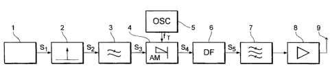
Figs. la, lb show in a block diagram, as the invention's preferred
20 embodiment example, a transmitter and receiver of a message transfer
system.
Figs. 2a to 2e show the digital input signal of the transmitter, as well as
several intermediary stages of the signal processing in the tr~n.~mitter up
25 to the transmission signal.
,
CA 02269212 1999-04-19
- 14 -
Figs. 3a to 3d show the received signal, as well as several intermediary
stages of the signal processing in the receiver, up to the demodulated
signal.
S Figs. 4a, 4b show in a block diagram the tr~nemitter and receiver of amessage transfer system with active transmission of high and low levels.
Figs. Sa to Sk show the digital input signal of the transmitter of Fig. 4a,
as well as several intermediary stages of the signal processing in the
10 tr~nemitter.
Figs. 6a to 6e show the signal picked up on the receiver side, as well as
several intermediary stages of the signal processing in the receiver.
lS Figs. 7, 8 each show a modified form of the receiver shown in Fig. 4b
with a noise suppression circuit.
Figs. 9a and 9b show graphical illustrations of the improvement in the
signal/noise ratio obtainable with this invention's method.
A transmitter, illustrated in Fig. la, serves in the tr~n.emi.esion of a signal
sl, generated by signal source 1 and present in a form that can be
digitized, across a noisy transmission path to thé receiver, illustrated in
Fig. lb, whereby, for predetermined requirements on range and noise
25 immllnity, the transmission can advantageously be made with relatively
low transmitting power, which on one hand increases the battery life for
battery operated transmitters, and on the other hand reduces the
. .
CA 02269212 1999-04-19 -~
environmental impact by electromagnetic radiation - also known as
Electro-smog. In addition, compared to other communications systems,
the error potential of the tr~n~milter is reduced due to the relatively low
transmission power.
S
In the transmitter, a digital input signal sl, the time behavior of which is
shown in detail in Fig. 2a, is at first fed to a pulse shaper 2, which
transforms the relatively wide square pulses of input signal s, to short
needle pulses, that are meant to emulate (quasi-) Dirac pulses. It can be
10 seen in the illustration of the needle pulse sequence s2 in Fig. 2b that the
generation of the individual needle pulses is triggered every time by the
rising edge of the square pulses of input signal sl.
A needle pulse sequence s2 generated in this m~nner is subsequently fed
15 to a low-pass filter 3, the delay time response of which possesses a peak
shortly before the critical frequency, so that the individual needle pulses
- as can be seen in Fig. 2c - are transformed to Sinc-pulses, the shape
of which col~orms to the well known Sinc-function Sinc(x) = sin(x) /x.
20 Subsequently the Sinc-pulse series S3 iS carried to an amplitude modulator
4, which modulates this signal onto a carrier o~scillation of frequency fT,
which is generated by oscillator 5, so that carrier frequency pulses with
a Sinc-shaped envelope are generated at the output of the amplitude
modulator 4, as illustrated in Fig. 2d. (For illustrative purposes the pulses
25 are shown broadened in the drawing, in reality, when shown to scale,
they are narrower).
CA 02269212 1999-04-19
- 16 -
A dispersion filter 6 is connected after the amplitude modulator 4, which
filters the modulated carrier frequency signal S4 according to its frequency
dependent, differential delay time characteristics. At the output of the
dispersion filter 6 arrive - as can be seen in Fig. 2e - linearly frequency
S modulated pulses with constant amplitude, the frequency of which
decreases during the pulse duration from a value fT+~f/2 above the
carrier frequency fT to a value fT-/~f/2 below the carrier frequency.
Thus in the transmitter shown here, the transmission of the input signal
10 sl is made unipolar, i.e. a transmission pulse is only generated for a high
level of the input signal sl, while a low level can be recognized from a
pause in the transmission signal S5. For this reason transmitter and
receiver can be constructed reasonably simply, each only cont~ining one
dispersion filter 6,13.
The pulse sequence s5 generated in this manner is subsequently fed to a
band-pass filter 7, the center frequency of which is equal to the carrier
frequency fT of the frequency modulated pulses, so that signals outside the
tr~n~mi~sion band are filtered out.
Finally, the band-pass limited signal is supplied to antenna 9 by a
transmitter amplifier 8 and emitted.
The receiver shown in Fig. lb allows the reception of the linearly
25 frequency modulated signal, emitted by the transmitter described above,
as well as the demodulation and recovery of the digital input signal S3 or
Sl .
CA 02269212 1999-04-19
For this, the signal received by the receiver's antenna 10 - for example
in diversity operation - is fed to a pre-amplifier 11 and subsequently a
band-pass filter l2, the center frequency of which is equal to the carrier
frequency fT of the band-pass limite~l tr~n.~mi~sion signal, so that noise
5 signals from-other frequency ranges can be filtered out of the receiver
signal. (Instead of a conventional band-pass filter a surface acoustic wave
filter can be used here.) The time behavior of the signal s6 prepared in
this manner is shown in detail in Fig. 3a, whereby for simplification a
noise free tr~n~mi.~sion path is assumed.
The received signal s6 consists of a series of linearly frequency modulated
pulses, whereby the frequency decreases during the pulse duration,
according to the modulation characteristic used on the transmitter side,
from a value fT+~f/2 above the carrier frequency fT to a value fT-~\f/2
15 below the carrier frequency.
Subsequently the signal s6 is fed to a dispersion filter 13, which time
compresses the individual pulses of the input signal s6, which leads to a
corresponding increase in amplitude, and thus an improved signal/noise
20 ratio.
Hereby the pulse compression utilizes the fact that the signal components
of higher frequency arrive at the output of the dispersion filter 13 before
the lower frequency signal components, due to the linear frequency
25 modulation carried out on the transmitter side. The dispersion filter 13
compensates for the "lead" of the higher frequency signal components by
delaying these more than the lower frequency signal components.
CA 02269212 1999-04-19
- 18 -
Hereby the frequency dependent, differential delay time response of
dispersion filter 13 is matched to the modulation characteristic of the
frequency modulation carried out on the tr~n~mit~er side, in such a
manner, that the spectral signal components of the received signal arrive
5 essentially coincident at the output of dispersion filter 13. As seen in
Fig. 3b, the spectral components superpose to form a signal S7 with Sinc-
shaped envelope for each pulse, whereby the amplitude of the individual
pulses is significantly increased compared to the received linear frequency
modulated signal s6. (It should be noted at this point that for improved
10 clarity a distortion was introduced in the schematic signal representations
shown in the figures. In reality the frequency-moclul~te-l pulses are closer
together and the compressed signals are much narrower.)
Subsequently the output signal of the dispersion filter 13 is fed to a
15 demodulator 14, which separates signal S7 from the high frequency carrier
oscillation and - as seen in Fig. 3c - generates a discrete output signal
s8 with needle shaped pulses.
Subsequently, the original digital signal S9, the time behavior of which is
20 shown in detail in Fig. 3d, is recovered from the needle shaped pulses
using a pulse shaper 15.
Figures 4a and 4b show a further message transfer system according to this
invention, which differs from the simpler embodiment example, described above
and illustrated in Figs. la and lb, most importantly by the fact that both the high
25 level as well as the low level of the digital information signal are tr~n~mitted
actively, which contributes to a higher noise immllnity.
The tr~n~mitt~-r shown in Fig. 4a contains a pulse shaper 17, which is triggered by
CA 02269212 1999-04-19
- 19 -
a timing generator 16, using timing pulses opposite in phase, shown in Figs. 5a,5b. At its output the pulse shaper emits - as shown in Fig 5c - a sequence g, ofneedle shaped pulses that form a (quasi-) Dirac delta sequence. The pulse
sequence gl gen~ted in this m~nner is subsequently fed to a low-pass filter 18,
5 the filter characteristic of which possesses a peak just before the critical frequency,
and that ~ srolll,s the needle shaped pulses to Sinc-shaped pulses, which are
shown in detail in Fig. 5d. Subsequently, this pulse sequence g2 is modulated onto
a carrier oscillation with carrier frequency fT, generated by the oscillator 19, using - -
an amplitude modulator 20. Thus, at the output of amplitude modulator 20 arrives10 a sequence g3 of equidistant carrier frequency pulses with Sinc-shaped envelopes.
It is important in this context, that the pulse sequence g3 arriving at the output of
the amplitude modulator 20 is independent of the digital input signal g4, and thus
does not contain any information.
15 Subsequently, the imprinting of the information of input signal g4 is
effected by means of an analogue switch 21, which is controlled by input
signal g4, and, depending on the amplitude of the input signal g4, directs
the pulse sequence g3, generated by amplitude modulator 20, either to a
dispersion filter 22 with a frequency dependent linearly decreasing delay
20 time, or to a dispersion filter 23 with a frequency dependent linearly
rising delay time. At their outputs, the dispersion filters 22, 23 are
connected to a further analogue switch 24 or a mixer stage, which,
depending on the amplitude of input signal g4, selects the output signal
g7, g8 of one of the two dispersion filters 22, 23 and passes it on.
Thus, at the output of the analogue switch 24 arrives - as shown in Fig.
Sk - a sequence gg of carrier frequency pulses, linearly frequency
modulated pulse by pulse, whereby for a high level of the input signal g4
the individual pulses show a linearly increasing frequency during the
CA 02269212 1999-04-19
- 20 -
pulse duration, whereas for a low level of input signal g4 the frequency
during the pulse decreases linearly.
The signal arriving at the output of analogue switch 24 is subsequently
5 filtered by a band-pass filter to suppress interference signals located
outside of the tr~n.~mi~sion band. The signal obtained in this m~nner is
then amplified by a tr~ncmitter amplifier 26 and is emitted by the
transmitter antenna 27.
10 Fig. 4b shows the associated receiver that receives the signal, emitted by
the transmitter shown in Fig. 4a, using an antenna 28. The receiver
amplifies the signal in a pre-amplifier 29, and in a band-pass filter 30
removes any interference signals, the frequency of which lies outside the
transmission band.
Subsequently, the received signal is carried to two dispersion filters 32,
33 by a ~wilclling element 31. Hereby the frequency dependent delay
time response of ~e two dispersion filters 32, 33 on the receiver side is
matched in pairs to the frequency dependent delay time response of the
20 two dispersion filters 22, 23 on the transmitter side, in such a way that
the spectral signal components of the received signal add to a pulse with
increased amplitude at the output of one of the two dispersion filters, 32
or 33, while only a time expanded pulse arrives at the output of the other
dispersion filter, 33 or 32.
As seen in Figs. 6a and 6b, the output signals g10 or gll of dispersion filters 32, 33
consist of a seql)enre of carrier frequency pulses with Sinc-shaped envelopes.
-
CA 02269212 1999-04-19
The signals g10 or gll, appearing at the output of the two dispersion f1lters
32, 33, are subsequently fed to a demodulator 34, 35, which separates
the signals g10 or gll from the carrier oscillation and generates needle
shaped pulses, as seen in Fig. 6c or 6d.
While each of the needle impulses at the output of demodulator 34 corresponds toone high level of ~e input signal g4, the needle impulses arriving at the output of
the other demodulator 35 in-lir.ate low levels of input signal g4
10 To recover the original input signal g4 from the two signals gl2, gl3, the
two signals gl2, g13 are fed to a timing generator 36 for triggering, which
generates a timing signal that reproduces the timing rate of the original
input signal g4. This timing signal, together with the output signals gl2,
g13 of the two demodulators 34, 35 is fed to the decoder 37, which
15 recovers the original output signals, g4, gl4, as can bee seen in Fig. 6e.
Fig. 7 shows a modified form of the receiver shown in Fig. 4b, with a
noise suppression circuit 38, which can be combined with other receivers
for such Chirp signals. Due to the very close similarity of this receiver
20 with the one shown in Fig. 4b, functionally equivalent components are
labeled by the same reference signs in the two figures.
As in the previously described receiver, the signal chirped on the
transmitter side is received through an antenna 28 and at first fed to an
25 input amplifier 15 and a band-pass filter 30, which is tuned to the carrier
frequency and thus filters out noise signals lying outside the transmission
band. Subsequently, the signal is carried to the noise suppression circuit
38 and split into two parallel branches, in each of which two dispersion
CA 02269212 1999-04-19
filters 39, 44 or 40, 43, inverse with respect to each other, are connected
in series. During an active tr~n~mi~sion of a logic LOW level as well as
of a logic HIGH level, one of the two dispersion filters, 39 or 40,
arranged on the input side, is tuned in such a way that a time compressed
S signal arrives at the output of this dispersion filter, 39 or 40. At the
output of the other dispersion filter, 39 or 40, arrives a pulse that is time
expanded to twice its original length. The two analogue switches 41, 42
intell~t the signal flow in the two branches symmetrically around the
center of the compressed pulse, so that the time compressed pulse is
10 suppressed and only the time expanded pulse in the other branch remains.
Hereby the analogue switches 41, 42 are controlled through the
synchronizing circuit 46, that is triggered by the timing generator 36, and
thus reproduces the timing of the output signal, and thus the tr~n~mi~sion
timing. The following dispersion filters 43, 44 generate the original
15 pulse, with original width and correspondingly also with original
amplitude, from the time expanded pulse. These pulses are then fed to
the subtracter 45, at the output of which appears essentially the original
pulse.
20 The matter is dirr~rent for the noise that is caused by the noisy
transmission path, and is received by the receiver together with the useful
signal. This noise is at first shifted into different directions by the
dispersion filters 39, 40. But the dispersion filter 43, 44, connected
after, reverse this shift, so that the input noise is reconstructed in the two
25 branches, except the very short portion cut out by the analogue switches
41, 42. Thus the subtraction by the subtracter 45 leads to extensive
suppression of the noise picked up on the receiver side.
CA 02269212 1999-04-19
The further processing of the signal that was prepared in this m~nner then
occurs as described in the description to Fig. 4b.
The receiver shown in Fig. 8 differs from the one described above and
5 illustrated in Fig. 7 essentially by the design and the controlling of the
noise suppression circuit 47. Due to the extensive similarity of the two
circuits, functionally equivalent components or component modules are
labeled by identical reference signs in Figs. 7 and 8.
10 As with the receiver shown in Fig. 7, the chirped pulses are received by the
antenna 28 and at first fed to an input ampli~ler 29 and a band-pass filter 30,
which is tuned to the carrier frequency and thus ~llters out noise sigr~ls lyingoutside ~e tr~n~mi~,cion band.
15 Subsequently the signal is carried to the noise suppression circuit 47,
which splits the signal into two parallel branches, that each contain two
dispersion filters 48, 52 and 49, 53, inverse with respect to each other,
connected in series. ~t the output of the noise suppression circuit 47 the
two branches are joined by the subtracter 54, whereby the noise in the
20 received signal is completely ~uppressed by the subtraction.
In contrast, the chirped signal is not cancelled~by the subtraction in the
subtracter 54, so that the signal/noise ratio is significantly increased.
Hereby the dispersion filters 48, 49 on the input side are matched to the
25 chirped signals, generated on the transmitter side, in such a way that a
time compressed pulse with correspondingly increased amplitude appears
at the output of one of the dispersion filters 48, 49, whereas a time
expanded pulse with correspondingly reduced amplitude appears at the
CA 02269212 1999-04-19
- 24 -
output of the other dispersion filter 49, 48. Upon arrival of the
compressed pulses, the signal flow in the two branches is suppressed
synchronously by the multipliers 50, 51, - as will be described in detail
- so that the compressed pulse is suppressed and there remains only the
5 time compressed pulse excluding the negligible short cut-out. The
original pulse is then generated from the time expanded pulse by the
dispersion filters 52, 53 connected after, so that essentially the originally
received signal, with a significantly improved signal to noise ratio,
arrives at the output of the subtracter 54.
The triggering of the multipliers 50, 51 occurs in fixed synchronization
with the tr~n~mi~sion timing rate, so that the signal in the two branches
of the noise suppression circuit 47 can be suppressed exactly at the
arrival of the time compressed pulse. For this, the receiver contains a
15 synchronizing circuit 57, which on the input side is connected to the
timing generator 36 for synchronization. Subsequently, Sinc-pulses with
amplitude 1, lying inverted with the peak towards to zero, are generated
by a pulse shaper 56 and a low-pass filter 55, and are then fed to the
multipliers 50, 51. The multipliers 50, 51 multiply the signals in the two
20 branches of the noise suppression circuit 47, either by zero or by unity,
which accordingly either suppresses the signal or leaves the signal to pass
essentially unchanged. Thus the multipliers 50, 51 here have the same
effect as the switching elements 41, 42 in the variation of the noise
suppression circuit 38 described before.
The scope of the invention is not limited to the previously listed preferred
embodiments. A multitude of variations is possible that make use of the
CA 02269212 1999-04-19
- 25 -
presented solution even in f~lnrl~mentally different implementations. The
embodiment examples shown here should only be seen as basic types of
a wide spectrum of solutions.
5 Figures 9a and 9b illustrate the improvement of the signal/noise ratio that
can be achieved by this invention for different expansion factors ~ = TT
/ ~, with TT as mean duration of a transmission pulse processed using the
"Chirp~ technique, and ~ as the mean duration of the pulse compressed
in the receiver. Fig. 9a shows the signal to noise ratio (S+N)/N at the
10 receiver output as a function of S/N at the receiver input, and Fig. 9b
shows the dependence of the relation (S+N)/N = f(S/N) norm~li7ed to
i.e. the degree of improvement as a function of the original
signal/noise ratio. Hereby, values in the range from 1 to 160 are selected
as parameter for ~.
The figures illustrate that the improvement that can be achieved becomes
larger with increasing pulse "expansion"/compression, and is especially
distinct for small original signal/noise ratios. This clearly documents that
the method can be lltili7e~1 advantageously in particular in strongly
20 interfering surrollnclin~.~, and/or for long transmission ranges, and/or for
low transmitting power.
.