Language selection

Search

Patent 2269346 Summary

Third-party information liability

Some of the information on this Web page has been provided by external sources. The Government of Canada is not responsible for the accuracy, reliability or currency of the information supplied by external sources. Users wishing to rely upon this information should consult directly with the source of the information. Content provided by external sources is not subject to official languages, privacy and accessibility requirements.

Claims and Abstract availability

Any discrepancies in the text and image of the Claims and Abstract are due to differing posting times. Text of the Claims and Abstract are posted:

  • At the time the application is open to public inspection;
  • At the time of issue of the patent (grant).
(12) Patent Application: (11) CA 2269346
(54) English Title: DC ENERGY FLOW DIRECTION CONTROL USING REVERSE BLOCKING DEVICES IN DC-AC INVERTERS
(54) French Title: COMMANDE DE LA DIRECTION DU COURANT CONTINU FAISANT APPEL A DES DISPOSITIFS DE BLOCAGE DU COURANT INVERSE DANS DES ONDULEURS
Status: Deemed Abandoned and Beyond the Period of Reinstatement - Pending Response to Notice of Disregarded Communication
Bibliographic Data
Abstracts

English Abstract


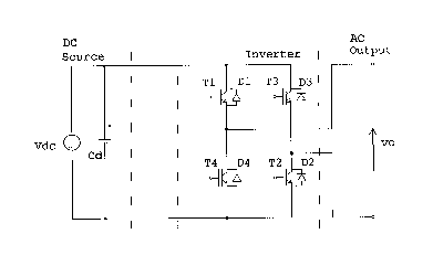
A DC-AC inverter is defined as an electrical instrument to convert a DC
(direct current) source to
an AC (alternating current) output. In such an instrument, the electric energy
can flow from the
DC source to the AC output, or from the AC output to the DC source. But the
latter energy-flow
direction is not the intentional design direction for the inverter. This
phenomenon exists when the
voltage level at the DC source is lower than the voltage level at the AC
output, for example, when
the inverter is used in the wind energy conversion systems at low wind
conditions, or when the
inverter is used in the photovoltaic solar energy conversion systems at cloudy
time. In such
systems, the AC output is connected to the electric power lines, or the
electric grid as the
technical term used by electric utilities. The energy-flow from the AC to the
DC can cause
substantial reactive power, usually in lagging form, interference with the
electric power delivery,
increasing energy losses and reducing the energy conversion efficiency of the
wind energy
conversion systems or photovoltaic solar energy conversion systems.
In this invention, the electric energy-flow unique direction from the DC to
the AC is secured by
adding a reverse blocking device, for example, a diode in series connection in
between the DC
source and the inverter. By adding such a reverse blocking device, for example
a diode, defined as
the blocking diode, the electric energy-flow is confined only from the DC
source to the AC output
no matter what the DC voltage level is. As a result, the reactive power output
of the inverter and
energy losses are reduced, and the system energy conversion efficiency is
increased. A small
fraction of the previous DC capacitance will be moved to the position after
the reverse blocking
device, or an additional capacitor will be added at the position after the
reverse blocking device to
smooth the inverter current commutation and reduce the voltage tension on the
inverter switching
devices. Other options to reduce the voltage tension may also include a
parallel connected switch
with the reverse blocking device and a voltage varistor.


Claims

Note: Claims are shown in the official language in which they were submitted.


The embodiments of the invention in which an exclusive property or privilege
is claimed
are defined as follows:
1. A reverse blocking device D0, such as a diode, added at the position in
series connection
in between the DC source and the inverter, to make a unique energy-flow
direction only
from the DC source to the AC output through the inverter.
2. The capacitor Cd is split into two parts either as Cd1=(1-n/m)Cd and
Cd2=(n/m)Cd,
n>m>0, and these two parts are positioned and connected at before and after
the reverse
blocking device as described in claim 1.
3. The capacitor Cd is kept at the position before the blocking diode as
described in claim 1,
and adding the second capacitor Cd2 at the position after the blocking diode
as described
in claim 1.
4. A bypass switch connected in parallel with the reverse blocking device as
described in
claim 1.
5. A voltage varistor connected in parallel with the Cd2 as described in claim
2 and claim 3.
6. A DC-AC inverter including the configurations as described in claim 1,
claim 2, claim 3,
claim 4, and claim 5.
5/8

Description

Note: Descriptions are shown in the official language in which they were submitted.


CA 02269346 1999-04-14
Specif canon
This invention relates to the energy conversion efficiency improvement and the
reduction of
reactive power output and energy losses of DC-AC inverters. This invention is
especially intended
to the wind energy electric conversion systems and the photovoltaic solar
energy electric
conversion systems.
A typical single-phase DC-AC inverter diagram is shown in Figure I (see page
6/8). The
switching devices shown, T1, T2, T3, and T4, are, but not necessary,
transistors as shown here
just for describing convenience. The switching devices can be any type, for
example, thyristors,
GTOs (gate turned-off thyristors), and IGBTs (insulated gate bipolar
transistors), etc. On the
2/8

CA 02269346 1999-04-14
other hand, this invention is intended not only on single-phase inverters, as
shown in Figure 1, but
also intended on the multi-phase inverters such as 3-phase inverters as shown
in Figure 3 (see
page 7/8). In Figure 1, the DC source represents any sources which can be used
to generate the
DC output, for example, a DC battery or any rectifiers' output, controlled or
uncontrolled,
controllable or uncontrollable, etc. Capacitor Cd is normally used in the DC-
AC inverters, and
functioned as: (1) a filter to smooth the DC source; (2) a part of inverter
current commutation
circuit. Diodes D1, D2, D3, and D4 are the other part of inverter current
commutation circuit.
If the DC voltage Vdc is higher than the AC voltage vo at any time, the DC
energy can be
directed from the DC source to the AC output by controlling the switching
devices T1, T2, T3,
and T4. But if Vdc is lower than vo at some time during the cycle and the AC
output is connected
to the electric power lines, such as in the case of wind energy electric
conversion systems, the AC
electric power will flow back to the DC source through D1, D2, D3, and D4.
This energy-flow-
back introduces substantial reactive power to the power lines from the
inverter, making significant
energy losses, reducing energy conversion efficiency, and resulting in less DC
source energy
converted and directed to the electric power lines.
I have found that these disadvantages may be overcome by adding a reverse
blocking device DO
such as a diode in series connection in between the DC source and the inverter
as shown in Figure
2 (see page 6/8) or in Figure 4 (see page 7/8). The diode, defined as the
blocking diode, confines
the electric energy-flow uniquely from the DC source to the AC output, and
there is no way to
allow the AC energy to flow back to the DC. The above disadvantages can
therefore be
overcome.
This blocking diode may cause the inverter current commutation dill'lculty.
This di~culty depends
on the switching algorithms - normally defined as the pulse width modulation
(P~
techniques. However, no matter what switching algorithms are employed, the
diil'lculty
introduced by the blocking diode may be overcome by splitting the previous DC
capacitor Cd into
two parts, Cdl= (1-m/n)Cd and Cd2=(m/n)Cd and connecting two parts ofthe
capacitor at the
positions before and after the blocking diode as shown in Figure 2 or Figure
4. Where n and m are
positive numbers (n>0, m>0), n is larger than m (n>m). The numbers n and m can
be properly
selected by computer simulation. For example, n=1-20/1000, m=20/1000. The
second method to
overcome the current commutation difficulty due to the blocking diode is that
the previous
capacitor Cd is kept at the position before the blocking diode as Cdl, and
adding the other
capacitor Cd2 after the blocking diode. The capacitance of Cd2 can be selected
by computer
simulation. Cd2 may not be necessary if certain type of PWM techniques are
employed. I have
found that a snubber capacitor (high frequency, high Q, low loss, non-
inductance or low
inductance) type may be selected for Cd2. To select a proper Cd2, I have found
the following
principle. A small value of Cd2 will help to overcome the disadvantages caused
by the low DC
voltage -- the smaller the Cd2 value, the better, but will introduce a higher
voltage tension on the
switching devices T 1 through T4. A larger Cd2 will help to reduce the voltage
tension but is not
good to overcome the disadvantages. Therefore, a compromise may be required to
decide the
value of Cd2.
3/8

CA 02269346 1999-04-14
Another option to overcome the voltage tension difficulty is to use a bypass
switch, S 1, connected
in parallel with the reverse blocking device DO as shown in Figure 5 and
Figure 6 (see page 8/8).
The switch S 1 can be any type, for example, the mechanical type, the electro-
magnetic type, the
solid type, and the semiconductor's type, etc. At low DC voltage conditions
when the voltage
tension on the switching devices is low, the bypass switch S 1 will be open to
secure the DC
energy-flow direction from the DC source to the AC output. At high DC voltage
conditions when
the voltage tension is high, S 1 can be closed to reduce the voltage tension.
A high DC voltage will
actually produce the correct energy-flow direction from the DC source to the
AC output.
A voltage varistor, VR, as shown in Figure S and Figure 6, connected in
parallel with the Cd2 can
provide another option to reduce the voltage tension on the switching devices
due to the
introduction of the reverse blocking device.
4/8

Representative Drawing
A single figure which represents the drawing illustrating the invention.
Administrative Status

2024-08-01:As part of the Next Generation Patents (NGP) transition, the Canadian Patents Database (CPD) now contains a more detailed Event History, which replicates the Event Log of our new back-office solution.

Please note that "Inactive:" events refers to events no longer in use in our new back-office solution.

For a clearer understanding of the status of the application/patent presented on this page, the site Disclaimer , as well as the definitions for Patent , Event History , Maintenance Fee  and Payment History  should be consulted.

Event History

Description Date
Inactive: IPC assigned 2020-04-03
Inactive: IPC expired 2007-01-01
Inactive: IPC removed 2006-12-31
Inactive: IPC from MCD 2006-03-12
Inactive: Dead - RFE never made 2005-04-14
Application Not Reinstated by Deadline 2005-04-14
Inactive: Payment - Insufficient fee 2005-03-10
Inactive: Delete abandonment 2005-03-10
Inactive: Payment - Insufficient fee 2005-03-10
Inactive: Adhoc Request Documented 2005-01-17
Inactive: Payment - Insufficient fee 2004-09-14
Inactive: Delete abandonment 2004-09-14
Inactive: Payment - Insufficient fee 2004-09-01
Inactive: Delete abandonment 2004-09-01
Deemed Abandoned - Failure to Respond to Maintenance Fee Notice 2004-04-14
Inactive: Payment - Insufficient fee 2004-04-14
Deemed Abandoned - Failure to Respond to Maintenance Fee Notice 2004-04-14
Inactive: Abandon-RFE+Late fee unpaid-Correspondence sent 2004-04-14
Deemed Abandoned - Failure to Respond to Maintenance Fee Notice 2004-04-14
Inactive: Payment - Insufficient fee 2004-04-13
Request for Examination Received 2004-03-22
Inactive: Adhoc Request Documented 2003-01-31
Application Published (Open to Public Inspection) 2000-10-14
Inactive: Cover page published 2000-10-13
Inactive: First IPC assigned 1999-06-03
Inactive: Office letter 1999-05-25
Inactive: Filing certificate - No RFE (English) 1999-05-20
Application Received - Regular National 1999-05-19

Abandonment History

Abandonment Date Reason Reinstatement Date
2004-04-14
2004-04-14
2004-04-14

Maintenance Fee

The last payment was received on 2005-04-07

Note : If the full payment has not been received on or before the date indicated, a further fee may be required which may be one of the following

  • the reinstatement fee;
  • the late payment fee; or
  • additional fee to reverse deemed expiry.

Patent fees are adjusted on the 1st of January every year. The amounts above are the current amounts if received by December 31 of the current year.
Please refer to the CIPO Patent Fees web page to see all current fee amounts.

Fee History

Fee Type Anniversary Year Due Date Paid Date
Application fee - small 1999-04-14
MF (application, 3rd anniv.) - small 03 2002-04-15 2001-03-12
MF (application, 2nd anniv.) - small 02 2001-04-16 2001-03-12
MF (application, 4th anniv.) - small 04 2003-04-14 2003-04-04
MF (application, 5th anniv.) - small 05 2004-04-14 2004-03-22
2004-06-14 2004-05-03
MF (application, 6th anniv.) - small 06 2005-04-14 2005-04-07
2005-04-07
Owners on Record

Note: Records showing the ownership history in alphabetical order.

Current Owners on Record
HONG HUANG
Past Owners on Record
None
Past Owners that do not appear in the "Owners on Record" listing will appear in other documentation within the application.
Documents

To view selected files, please enter reCAPTCHA code :


To view images, click a link in the Document Description column (Temporarily unavailable). To download the documents, select one or more checkboxes in the first column and then click the "Download Selected in PDF format (Zip Archive)" or the "Download Selected as Single PDF" button.

List of published and non-published patent-specific documents on the CPD .

If you have any difficulty accessing content, you can call the Client Service Centre at 1-866-997-1936 or send them an e-mail at CIPO Client Service Centre.

({010=All Documents, 020=As Filed, 030=As Open to Public Inspection, 040=At Issuance, 050=Examination, 060=Incoming Correspondence, 070=Miscellaneous, 080=Outgoing Correspondence, 090=Payment})


Document
Description 
Date
(yyyy-mm-dd) 
Number of pages   Size of Image (KB) 
Representative drawing 2000-10-10 1 4
Abstract 1999-04-13 1 55
Description 1999-04-13 3 130
Claims 1999-04-13 1 30
Drawings 1999-04-13 3 63
Filing Certificate (English) 1999-05-19 1 165
Notice: Maintenance Fee Reminder 2001-01-15 1 121
Notice: Maintenance Fee Reminder 2003-01-14 1 115
Reminder - Request for Examination 2003-12-15 1 123
Notice: Maintenance Fee Reminder 2004-01-14 1 116
Notice of Insufficient fee payment (English) 2004-04-12 1 92
Notice of Insufficient fee payment (English) 2004-04-13 1 92
Courtesy - Abandonment Letter (Request for Examination) 2004-08-22 1 166
Second Notice: Maintenance Fee Reminder 2004-10-17 1 122
Notice: Maintenance Fee Reminder 2005-01-16 1 118
Correspondence 1999-05-20 1 22
Correspondence 2003-01-14 4 148
Fees 2003-04-03 1 48
Fees 2001-03-11 2 80
Fees 2004-03-21 1 23
Fees 2004-05-02 1 31
Correspondence 2004-08-31 6 237
Fees 2005-04-06 3 153