Sélection de la langue

Search

Sommaire du brevet 2269346 

Énoncé de désistement de responsabilité concernant l'information provenant de tiers

Une partie des informations de ce site Web a été fournie par des sources externes. Le gouvernement du Canada n'assume aucune responsabilité concernant la précision, l'actualité ou la fiabilité des informations fournies par les sources externes. Les utilisateurs qui désirent employer cette information devraient consulter directement la source des informations. Le contenu fourni par les sources externes n'est pas assujetti aux exigences sur les langues officielles, la protection des renseignements personnels et l'accessibilité.

Disponibilité de l'Abrégé et des Revendications

L'apparition de différences dans le texte et l'image des Revendications et de l'Abrégé dépend du moment auquel le document est publié. Les textes des Revendications et de l'Abrégé sont affichés :

  • lorsque la demande peut être examinée par le public;
  • lorsque le brevet est émis (délivrance).
(12) Demande de brevet: (11) CA 2269346
(54) Titre français: COMMANDE DE LA DIRECTION DU COURANT CONTINU FAISANT APPEL A DES DISPOSITIFS DE BLOCAGE DU COURANT INVERSE DANS DES ONDULEURS
(54) Titre anglais: DC ENERGY FLOW DIRECTION CONTROL USING REVERSE BLOCKING DEVICES IN DC-AC INVERTERS
Statut: Réputée abandonnée et au-delà du délai pour le rétablissement - en attente de la réponse à l’avis de communication rejetée
Données bibliographiques
Abrégés

Abrégé anglais


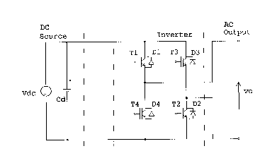
A DC-AC inverter is defined as an electrical instrument to convert a DC
(direct current) source to
an AC (alternating current) output. In such an instrument, the electric energy
can flow from the
DC source to the AC output, or from the AC output to the DC source. But the
latter energy-flow
direction is not the intentional design direction for the inverter. This
phenomenon exists when the
voltage level at the DC source is lower than the voltage level at the AC
output, for example, when
the inverter is used in the wind energy conversion systems at low wind
conditions, or when the
inverter is used in the photovoltaic solar energy conversion systems at cloudy
time. In such
systems, the AC output is connected to the electric power lines, or the
electric grid as the
technical term used by electric utilities. The energy-flow from the AC to the
DC can cause
substantial reactive power, usually in lagging form, interference with the
electric power delivery,
increasing energy losses and reducing the energy conversion efficiency of the
wind energy
conversion systems or photovoltaic solar energy conversion systems.
In this invention, the electric energy-flow unique direction from the DC to
the AC is secured by
adding a reverse blocking device, for example, a diode in series connection in
between the DC
source and the inverter. By adding such a reverse blocking device, for example
a diode, defined as
the blocking diode, the electric energy-flow is confined only from the DC
source to the AC output
no matter what the DC voltage level is. As a result, the reactive power output
of the inverter and
energy losses are reduced, and the system energy conversion efficiency is
increased. A small
fraction of the previous DC capacitance will be moved to the position after
the reverse blocking
device, or an additional capacitor will be added at the position after the
reverse blocking device to
smooth the inverter current commutation and reduce the voltage tension on the
inverter switching
devices. Other options to reduce the voltage tension may also include a
parallel connected switch
with the reverse blocking device and a voltage varistor.

Revendications

Note : Les revendications sont présentées dans la langue officielle dans laquelle elles ont été soumises.


The embodiments of the invention in which an exclusive property or privilege
is claimed
are defined as follows:
1. A reverse blocking device D0, such as a diode, added at the position in
series connection
in between the DC source and the inverter, to make a unique energy-flow
direction only
from the DC source to the AC output through the inverter.
2. The capacitor Cd is split into two parts either as Cd1=(1-n/m)Cd and
Cd2=(n/m)Cd,
n>m>0, and these two parts are positioned and connected at before and after
the reverse
blocking device as described in claim 1.
3. The capacitor Cd is kept at the position before the blocking diode as
described in claim 1,
and adding the second capacitor Cd2 at the position after the blocking diode
as described
in claim 1.
4. A bypass switch connected in parallel with the reverse blocking device as
described in
claim 1.
5. A voltage varistor connected in parallel with the Cd2 as described in claim
2 and claim 3.
6. A DC-AC inverter including the configurations as described in claim 1,
claim 2, claim 3,
claim 4, and claim 5.
5/8

Description

Note : Les descriptions sont présentées dans la langue officielle dans laquelle elles ont été soumises.


CA 02269346 1999-04-14
Specif canon
This invention relates to the energy conversion efficiency improvement and the
reduction of
reactive power output and energy losses of DC-AC inverters. This invention is
especially intended
to the wind energy electric conversion systems and the photovoltaic solar
energy electric
conversion systems.
A typical single-phase DC-AC inverter diagram is shown in Figure I (see page
6/8). The
switching devices shown, T1, T2, T3, and T4, are, but not necessary,
transistors as shown here
just for describing convenience. The switching devices can be any type, for
example, thyristors,
GTOs (gate turned-off thyristors), and IGBTs (insulated gate bipolar
transistors), etc. On the
2/8

CA 02269346 1999-04-14
other hand, this invention is intended not only on single-phase inverters, as
shown in Figure 1, but
also intended on the multi-phase inverters such as 3-phase inverters as shown
in Figure 3 (see
page 7/8). In Figure 1, the DC source represents any sources which can be used
to generate the
DC output, for example, a DC battery or any rectifiers' output, controlled or
uncontrolled,
controllable or uncontrollable, etc. Capacitor Cd is normally used in the DC-
AC inverters, and
functioned as: (1) a filter to smooth the DC source; (2) a part of inverter
current commutation
circuit. Diodes D1, D2, D3, and D4 are the other part of inverter current
commutation circuit.
If the DC voltage Vdc is higher than the AC voltage vo at any time, the DC
energy can be
directed from the DC source to the AC output by controlling the switching
devices T1, T2, T3,
and T4. But if Vdc is lower than vo at some time during the cycle and the AC
output is connected
to the electric power lines, such as in the case of wind energy electric
conversion systems, the AC
electric power will flow back to the DC source through D1, D2, D3, and D4.
This energy-flow-
back introduces substantial reactive power to the power lines from the
inverter, making significant
energy losses, reducing energy conversion efficiency, and resulting in less DC
source energy
converted and directed to the electric power lines.
I have found that these disadvantages may be overcome by adding a reverse
blocking device DO
such as a diode in series connection in between the DC source and the inverter
as shown in Figure
2 (see page 6/8) or in Figure 4 (see page 7/8). The diode, defined as the
blocking diode, confines
the electric energy-flow uniquely from the DC source to the AC output, and
there is no way to
allow the AC energy to flow back to the DC. The above disadvantages can
therefore be
overcome.
This blocking diode may cause the inverter current commutation dill'lculty.
This di~culty depends
on the switching algorithms - normally defined as the pulse width modulation
(P~
techniques. However, no matter what switching algorithms are employed, the
diil'lculty
introduced by the blocking diode may be overcome by splitting the previous DC
capacitor Cd into
two parts, Cdl= (1-m/n)Cd and Cd2=(m/n)Cd and connecting two parts ofthe
capacitor at the
positions before and after the blocking diode as shown in Figure 2 or Figure
4. Where n and m are
positive numbers (n>0, m>0), n is larger than m (n>m). The numbers n and m can
be properly
selected by computer simulation. For example, n=1-20/1000, m=20/1000. The
second method to
overcome the current commutation difficulty due to the blocking diode is that
the previous
capacitor Cd is kept at the position before the blocking diode as Cdl, and
adding the other
capacitor Cd2 after the blocking diode. The capacitance of Cd2 can be selected
by computer
simulation. Cd2 may not be necessary if certain type of PWM techniques are
employed. I have
found that a snubber capacitor (high frequency, high Q, low loss, non-
inductance or low
inductance) type may be selected for Cd2. To select a proper Cd2, I have found
the following
principle. A small value of Cd2 will help to overcome the disadvantages caused
by the low DC
voltage -- the smaller the Cd2 value, the better, but will introduce a higher
voltage tension on the
switching devices T 1 through T4. A larger Cd2 will help to reduce the voltage
tension but is not
good to overcome the disadvantages. Therefore, a compromise may be required to
decide the
value of Cd2.
3/8

CA 02269346 1999-04-14
Another option to overcome the voltage tension difficulty is to use a bypass
switch, S 1, connected
in parallel with the reverse blocking device DO as shown in Figure 5 and
Figure 6 (see page 8/8).
The switch S 1 can be any type, for example, the mechanical type, the electro-
magnetic type, the
solid type, and the semiconductor's type, etc. At low DC voltage conditions
when the voltage
tension on the switching devices is low, the bypass switch S 1 will be open to
secure the DC
energy-flow direction from the DC source to the AC output. At high DC voltage
conditions when
the voltage tension is high, S 1 can be closed to reduce the voltage tension.
A high DC voltage will
actually produce the correct energy-flow direction from the DC source to the
AC output.
A voltage varistor, VR, as shown in Figure S and Figure 6, connected in
parallel with the Cd2 can
provide another option to reduce the voltage tension on the switching devices
due to the
introduction of the reverse blocking device.
4/8

Dessin représentatif
Une figure unique qui représente un dessin illustrant l'invention.
États administratifs

2024-08-01 : Dans le cadre de la transition vers les Brevets de nouvelle génération (BNG), la base de données sur les brevets canadiens (BDBC) contient désormais un Historique d'événement plus détaillé, qui reproduit le Journal des événements de notre nouvelle solution interne.

Veuillez noter que les événements débutant par « Inactive : » se réfèrent à des événements qui ne sont plus utilisés dans notre nouvelle solution interne.

Pour une meilleure compréhension de l'état de la demande ou brevet qui figure sur cette page, la rubrique Mise en garde , et les descriptions de Brevet , Historique d'événement , Taxes périodiques et Historique des paiements devraient être consultées.

Historique d'événement

Description Date
Inactive : CIB attribuée 2020-04-03
Inactive : CIB expirée 2007-01-01
Inactive : CIB enlevée 2006-12-31
Inactive : CIB de MCD 2006-03-12
Inactive : Morte - RE jamais faite 2005-04-14
Demande non rétablie avant l'échéance 2005-04-14
Inactive : Paiement - Taxe insuffisante 2005-03-10
Inactive : Supprimer l'abandon 2005-03-10
Inactive : Paiement - Taxe insuffisante 2005-03-10
Inactive : Demande ad hoc documentée 2005-01-17
Inactive : Paiement - Taxe insuffisante 2004-09-14
Inactive : Supprimer l'abandon 2004-09-14
Inactive : Paiement - Taxe insuffisante 2004-09-01
Inactive : Supprimer l'abandon 2004-09-01
Réputée abandonnée - omission de répondre à un avis sur les taxes pour le maintien en état 2004-04-14
Inactive : Paiement - Taxe insuffisante 2004-04-14
Réputée abandonnée - omission de répondre à un avis sur les taxes pour le maintien en état 2004-04-14
Inactive : Abandon.-RE+surtaxe impayées-Corr envoyée 2004-04-14
Réputée abandonnée - omission de répondre à un avis sur les taxes pour le maintien en état 2004-04-14
Inactive : Paiement - Taxe insuffisante 2004-04-13
Requête d'examen reçue 2004-03-22
Inactive : Demande ad hoc documentée 2003-01-31
Demande publiée (accessible au public) 2000-10-14
Inactive : Page couverture publiée 2000-10-13
Inactive : CIB en 1re position 1999-06-03
Inactive : Lettre officielle 1999-05-25
Inactive : Certificat de dépôt - Sans RE (Anglais) 1999-05-20
Demande reçue - nationale ordinaire 1999-05-19

Historique d'abandonnement

Date d'abandonnement Raison Date de rétablissement
2004-04-14
2004-04-14
2004-04-14

Taxes périodiques

Le dernier paiement a été reçu le 2005-04-07

Avis : Si le paiement en totalité n'a pas été reçu au plus tard à la date indiquée, une taxe supplémentaire peut être imposée, soit une des taxes suivantes :

  • taxe de rétablissement ;
  • taxe pour paiement en souffrance ; ou
  • taxe additionnelle pour le renversement d'une péremption réputée.

Les taxes sur les brevets sont ajustées au 1er janvier de chaque année. Les montants ci-dessus sont les montants actuels s'ils sont reçus au plus tard le 31 décembre de l'année en cours.
Veuillez vous référer à la page web des taxes sur les brevets de l'OPIC pour voir tous les montants actuels des taxes.

Historique des taxes

Type de taxes Anniversaire Échéance Date payée
Taxe pour le dépôt - petite 1999-04-14
TM (demande, 3e anniv.) - petite 03 2002-04-15 2001-03-12
TM (demande, 2e anniv.) - petite 02 2001-04-16 2001-03-12
TM (demande, 4e anniv.) - petite 04 2003-04-14 2003-04-04
TM (demande, 5e anniv.) - petite 05 2004-04-14 2004-03-22
2004-06-14 2004-05-03
TM (demande, 6e anniv.) - petite 06 2005-04-14 2005-04-07
2005-04-07
Titulaires au dossier

Les titulaires actuels et antérieures au dossier sont affichés en ordre alphabétique.

Titulaires actuels au dossier
HONG HUANG
Titulaires antérieures au dossier
S.O.
Les propriétaires antérieurs qui ne figurent pas dans la liste des « Propriétaires au dossier » apparaîtront dans d'autres documents au dossier.
Documents

Pour visionner les fichiers sélectionnés, entrer le code reCAPTCHA :


Pour visualiser une image, cliquer sur un lien dans la colonne description du document (Temporairement non-disponible). Pour télécharger l'image (les images), cliquer l'une ou plusieurs cases à cocher dans la première colonne et ensuite cliquer sur le bouton "Télécharger sélection en format PDF (archive Zip)" ou le bouton "Télécharger sélection (en un fichier PDF fusionné)".

Liste des documents de brevet publiés et non publiés sur la BDBC .

Si vous avez des difficultés à accéder au contenu, veuillez communiquer avec le Centre de services à la clientèle au 1-866-997-1936, ou envoyer un courriel au Centre de service à la clientèle de l'OPIC.

({010=Tous les documents, 020=Au moment du dépôt, 030=Au moment de la mise à la disponibilité du public, 040=À la délivrance, 050=Examen, 060=Correspondance reçue, 070=Divers, 080=Correspondance envoyée, 090=Paiement})


Description du
Document 
Date
(aaaa-mm-jj) 
Nombre de pages   Taille de l'image (Ko) 
Dessin représentatif 2000-10-10 1 4
Abrégé 1999-04-13 1 55
Description 1999-04-13 3 130
Revendications 1999-04-13 1 30
Dessins 1999-04-13 3 63
Certificat de dépôt (anglais) 1999-05-19 1 165
Avis de rappel: Taxes de maintien 2001-01-15 1 121
Avis de rappel: Taxes de maintien 2003-01-14 1 115
Rappel - requête d'examen 2003-12-15 1 123
Avis de rappel: Taxes de maintien 2004-01-14 1 116
Avis de paiement insuffisant pour taxe (anglais) 2004-04-12 1 92
Avis de paiement insuffisant pour taxe (anglais) 2004-04-13 1 92
Courtoisie - Lettre d'abandon (requête d'examen) 2004-08-22 1 166
Deuxième avis de rappel: taxes de maintien 2004-10-17 1 122
Avis de rappel: Taxes de maintien 2005-01-16 1 118
Correspondance 1999-05-20 1 22
Correspondance 2003-01-14 4 148
Taxes 2003-04-03 1 48
Taxes 2001-03-11 2 80
Taxes 2004-03-21 1 23
Taxes 2004-05-02 1 31
Correspondance 2004-08-31 6 237
Taxes 2005-04-06 3 153