Note: Descriptions are shown in the official language in which they were submitted.
CA 02269539 1999-03-30
WO 98I20496 PCTNS97120373
SPIN DEPENDENT TUNNELING MEMORY
BACKGROUND OF THE INVENTION
The present invention relates to ferromagnetic thin-film
structures exhibiting relatively large magnetoresistive characteristics and,
more
particularly, to such structures used for the storage and retrieval of digital
data.
Many kinds of electronic systems make use of magnetic devices
including both digital systems, such as memories) and analog systems such as
magnetic field sensors. Digital data memories are used extensively in digital
systems of many kinds including computers and computer systems components, and
digital signal processing systems. Such memories can be advantageously based
on
the storage of digital symbols as alternative states of magnetization in
magnetic
materials provided in each memory storage cell) the result being memories
which
use less electrical power and do not lose information upon removals of such
electrical power.
Such memory cells, and magnetic field sensors also, can often be
advantageously fabricated using ferromagnetic thin-film materials, and are
often
based on magnetoresistive sensing of magnetic states, or magnetic conditions)
therein. Such devices may be provided on a surface of a monolithic integrated
circuit to provide convenient electrical interconnections between the device
and the
operating circuitry therefor.
Ferromagnetic thin-film memory cells, for instance) can be made
very small and packed very closely together to achieve a significant density
of
information storage) particularly when so provided on the surface of a
monolithic
integrated circuit. In this situation) the magnetic environment can become
quite
complex with fields in any one memory cell affecting the film portions in
neighboring memory cells. Also, small ferromagnetic film portions in a memory
cell can lead to substantial demagnetization fields which can cause
instabilities in
the magnetization state desired in such a cell.
A 19
CA 02269539 1999-03-30
WO 98I20496 PCT/US97/20373
-2-
These magnetic effects between neighbors in an array of closely
packed ferromagnetic thin-film memory cells can be ameliorated to a
considerable
extent by providing a memory cell based on an intermediate separating material
having two major surfaces on each of which an anisotropic ferromagnetic memory
thin-film is provided. Such an arrangement provides significant "flux
closure," i.e.
a more closely confined magnetic flux path, to thereby confine the magnetic
field
arising in the cell to affecting primarily just that cell. This result is
considerably
enhanced by choosing the separating material in the ferromagnetic thin-film
memory cells to each be sufficiently thin. Similar "sandwich" structures are
also
used in magnetic sensors.
In the recent past, reducing the thicknesses of the ferromagnetic thin-
films and the intermediate layers in extended "sandwich" structures, and
adding
possibly alternating ones of such films and layers, i.e. superlattices, have
been
shown to lead to a "giant magnetoresistive effect" being present in some
circumstances. This effect yields a magnetoresistive response which can be in
the
range of up to an order of magnitude or more greater than that due to the well
known anisotropic magnetoresistive response.
In the ordinary anisotropic magnetoresistive response, varying the
difference occurring between the direction of the magnetization vector in a
ferromagnetic thin-film and the direction of sensing currents passed through
that
film leads to varying effective electrical resistance in the film in the
direction of the
current. The maximum electrical resistance occurs when the magnetization
vector
in the field and the current direction therein are parallel to one another,
while the
minimum resistance occurs when they are perpendicular to one another. The
total
electrical resistance in such a magnetoresistive ferromagnetic film can be
shown to
be given by a constant value, representing the minimum resistance, plus an
additional value depending on the angle between the current direction in the
film
and the magnetization vector therein. This additional resistance has a
magnitude
characteristic that follows the square of the cosine of that angle.
CA 02269539 1999-03-30
WO 98I20496 PCT/L1S97/20373
-3-
Operating magnetic fields imposed externally can be used to vary the
angle of the magnetization vector in such a film portion with respect to the
easy
axis of that film. Such an axis comes about in the film because of an
anisotropy
therein typically resulting from depositing the film during fabrication in the
presence of an external magnetic field oriented in the plane of the film along
the
direction desired for the easy axis in the resulting film. During subsequent
operation of the device having this resulting film, such operational magnetic
fields
imposed externally can be used to vary the angle to such an extent as to cause
switching of the film magnetization vector between two stable states which
occur
for the magnetization being oriented in opposite directions along the film's
easy
axis. The state of the magnetization vector in such a film can be measured, or
sensed) by the change in resistance encountered by current directed through
this
film portion. This arrangement has provided the basis for a ferromagnetic)
magnetoresistive anisotropic thin-film to serve as a memory cell.
In contrast to this arrangement, the resistance in the plane of a
ferromagnetic thin-film is isotropic for the giant magnetoresistive effect
rather than
depending on the direction of the sensing current therethrough as for the
anisotropic
magnetoresistive effect. The giant magnetoresistive effect involves a change
in the
electrical resistance of the structure thought to come about from the passage
of
conduction electrons between the ferromagnetic layers in the "sandwich"
structure,
or superlattice structure, through the separating nonmagnetic layers with the
resulting scattering occurring at the layer interfaces, and in the
ferromagnetic layers,
being dependent on the electron spins. The magnetization dependant component
of the resistance in connection with this effect varies as the sine of the
absolute
value of half the angle between the magnetization vectors in the ferromagnetic
thin-
films provided on either side of an intermediate nonmagnetic layer. The
electrical
resistance in the giant magnetoresistance effect through the "sandwich" or
superlattice structure is lower if the magnetizations in the separated
ferromagnetic
thin-films are parallel and oriented in the same direction than it is if these
CA 02269539 1999-03-30
WO 98I20496 PCT/L1S97120373
-4-
magnetizations are antiparallel, i.e. oriented in opposing or partially
opposing
directions. Further) the anisotropic magnetoresistive effect in very thin
films is
considerably reduced from the bulk values therefor in thicker films due to
surface
scattering, whereas a significant giant magnetoresistive effect is obtained
only in
very thin films. Nevertheless) the anisotropic magnetoresistive effect remains
present in the films used in giant magnetoresistive effect structures.
As indicated above) the giant magnetoresistive effect can be
increased by adding further alternate intermediate nonmagnetic and
ferromagnetic
thin-film layers to extend a "sandwich" structure into a stacked structure,
i.e. a
superlattice structure. The giant magnetoresistive effect is sometimes called
the
"spin valve effect" in view of the explanation that a larger fraction of
conduction
electrons are allowed to move more freely from one ferromagnetic thin-film
Iayer
to another if the magnetizations in those layers are parallel than if they are
antiparallel or partially antiparallel to thereby result in the magnetization
states of
the layers acting as sort of a "valve."
Thus, a digital data memory cell based on the use of structures
exhibiting the giant magnetoresistive effect is attractive as compared to
structures
based on use of an anisotropic magnetoresistive effect because of the larger
signals
obtainable in information retrieval operatians with respect to such cells.
Such
larger magnitude signals are easier to detect without error in the presence of
noise
thereby leading to less critical requirements on the retrieval operation
circuitry.
A memory cell structure suitable for permitting the storing and
retaining of a digital bit of information, and for permitting retrieving same
therefrom has been demonstrated based on a multiple layer "sandwich"
construction
in a rectangular solid. This cell has a pair of ferromagnetic layers of equal
thickness
and area separated by a conductive nonmagnetic layer of the same shape and
area
parallel to the ferromagnetic layers but of smaller thickness. These
ferromagnetic
layers are each a composite layer formed of two strata each of a different
magnetic
material, there being a relatively thin ferromagnetic stratum in each of the
CA 02269539 1999-03-30
WO 98l20496 PCT/US97/20373
-5-
composite layers adjacent the nonmagnetic layer and a thicker ferromagnetic
stratum in each of the composite layers adjacent the thin ferromagnetic
stratum
therein. The ferromagnetic material of the thick stratum in one of the
composite
layers is the same as that in the thin stratum in the other composite layer)
and the
ferromagnetic material of the than stratum in the first composite layer is the
same
as the ferromagnetic material in the thick stratum of the second composite
layer.
Each of the composite layers is fabricated in the presence of a magnetic field
so as
to result in having an easy axis parallel to the long sides of the rectangular
solid.
The dimensions of the cell structure were lOpm in length and Sllm in width
with
a nonmagnetic layer of thickness 30A. The composite ferromagnetic layers are
each
formed of a 15~ thin stratum and a 401 thick stratum.
Thus, this memory cell structure has a pair of ferromagnetic layers
of matching geometries but different magnetic materials in the strata therein
to
result in one such layer having effectively a greater saturation magnetization
and a
greater anisotropy field than the other to result in different coercivities in
each. In
addition, the structure results in a coupling of the magnetization between the
two
ferromagnetic layers therein due to exchange coupling between them leading to
the
magnetizations in each paralleling one another in the absence of any applied
magnetic fields. As a result, the electrical resistance of the cell along its
length
versus applied magnetic f elds in either direction parallel thereto is
represented by
two characteristics depending on the magnetization history of the cell. Each
of
these characteristics exhibits a peak in this resistance for applied
longitudinal fields
having absolute values that are somewhat greater than zero) one of these
characteristics exhibiting its peak for positive applied longitudinal fields
and the
other characteristic exhibiting its peak for negative applied longitudinal
fields. The
characteristic followed by the resistance of the cell for relatively small
applied
longitudinal fields depends on which direction the magnetization is oriented
along
the easy axis for the one of the two ferromagnetic layers having the larger
coercivity. Thus, by setting the magnetization of the layer with the higher
CA 02269539 1999-03-30
WO 98I20496 PCT/US97120373
-6-
coercivity) a bit of digital information can be stored and retained) and the
value of
that bit can be retrieved without affecting this retention through a
deternunation of
which characteristic the resistance follows for a relatively small applied
longitudinal field.
S Such memory cell behavior for this structure can be modeled by
assuming that the ferromagnetic layers therein are each a single magnetic
domain
so that positioning of the magnetization vectors in the ferromagnetic layers
is based
on coherent rotation, and that uniaxial anisotropies characterize those
layers. The
angles of the magnetization vectors in the two ferromagnetic layers with
respect to
the easy axis in those layers are then found by minimizing the magnetic energy
of
these anisotropies summed with that due to the applied external fields and to
exchange coupling. That total energy per unit volume is then
E To, = E, + E Z + E,2
=K~,sin28,-Mb,Hcos~'Y-A,
+K~2 sinz92-M52H cos~'~'-92~
+A,z cos~9, -82~.
Here, K", and K"2 are anisotropy constants) A,2 is the exchange constant, MS,
and
MSZ are the magnetization saturation values, and H is the externally applied
field.
As indicated above, once the magnetization vectors have taken an angular
position
with respect to the easy axis of the corresponding layer at a minimum in the
above
indicated energy, the effective resistance between the ends of the memory cell
structure is determined by the net angle between the magnetization vectors in
each
of these layers.
Because of the assumption of single domain behavior in the
ferromagnetic layers, the above equation would seemingly be expected to
improve
its approximation of the assistant total magnetic energy as the length and
width of
CA 02269539 1999-03-30
VlrO 98/2Q496 PCT/US97/20373
that memory cell structure decreased toward having submicron dimensions.
However) this mode of operation described for providing the two
magnetoresistive
characteristics based on the history of the layer magnetizations) in depending
on the
differing anisotropy fields in the two ferromagnetic layers because of the
differing
materials used therein, becomes less and less reliable as these dimensions
decrease.
This appears to occur because decreasing the cell dimensions gives rise to
larger
and larger demagnetizing fields in the two ferromagnetic layers which) at some
point, overwhelm the effects of the anisotropy fields so that the above
described
behavior no longer occurs as described. In addition, the magnetizations of the
two
ferromagnetic layers rotate together under the influences of externally
applied fields
at angles with respect to the corresponding easy axis at angular magnitudes
much
more nearly equal to one another because of the increasing demagnetization
fields
in these layers as the dimensions thereof decrease. As a result, these
ferromagnetic
layers are less and less able to have the magnetizations thereof switch
directions of
orientation independently of one another as the dimensions thereof decrease so
that
the structure they are in becomes less able to provide the above described
memory
function in relying on only these ferromagnetic layer anisotropy differences.
An alternative memory cell structure which is more suited to
submicron dimensions is a cell of the kind described above exhibiting "giant
magnetoresistive effect" but which has the two composite ferromagnetic layers
formed of different thicknesses in the thick strata therein. Thus) the thick
strata in
one might be on the order of 40~ while that of the other might be on the order
of
55~ as an example. In this structure, reducing the size to submicron
dimensions
uses the shape anisotropy introduced by this thickness difference to provide
different switching thresholds for each of the ferromagnetic composite layers
in
response to externally applied operating magnetic fields. The shape anisotropy
leads to the effect of the demagnetizing field of one layer affecting the
switching
threshold of the other after the former layer has switched its magnetization
direction. As a result, the thicker ferromagnetic layer has a magnetization
which
CA 02269539 1999-03-30
WO 98/2049b PCT/US97120373
_g_
is fixed in orientation for externally applied operating magnetic fields that
are just
sufficient to switch the thinner ferromagnetic composite layer but not great
enough
to switch the magnetization of the thicker ferromagnetic composite layer. In
effect,
the demagnetizing fields as the device becomes sufficiently small dominate the
anisotropy fields that result from the deposition of the ferromagnetic layers
in the
presence of a magnetic field.
In the absence of externally applied operating magnetic field) the two
composite ferromagnetic layers have the magnetizations therein pointing in
opposite directions, i.e. they are antiparallel to one another) to result in
the structure
as a whole having relatively small cell demagnetizing fields and small
external stray
fields to affect the nearby mernory cells. The direction of magnetization in
the
thicker ferromagnetic composite layer is used to store the digital information
which
can only be changed in direction by externally applied fields great enough to
switch
magnetization directions in both composite ferromagnetic layers. That is,
storing
new information in the cell requires that the thicker ferromagnetic layer be
capable
of having the magnetization direction therein switched to be in accord with
the
incoming digital data.
Retrieving information from such a memory cell is accomplished by
switching the magnetization direction of the thinner ferromagnetic composite
layer
only as a basis for determining in which direction relative to the thinner
layer is the
magnetization oriented in the thicker layer. Typically) both such storing and
retrieving has meant that there needs to be a pair of external conductors
which can
coincidentally supply current to result in a field large enough to switch the
magnetization of the thicker ferromagnetic composite layer, but with that
current
in either conductor alone being able to generate fields only sufficient to
switch the
threshold of the thinner ferromagnetic layer. In some situations) only a
single
external conductor need be provided for this purpose because the sense current
used
in retrieving information from the memory cell can provide the coincident
current
needed with the current in the external conductor to switch the magnetization
CA 02269539 1999-03-30
WO 98I20496 PCT/US97120373
-9-
direction of the thicker ferromagnetic layer. Such a memory cell is described
in an
earlier filed co-pending application by A. Pohm and B. Everitt entitled "Giant
Magnetoresistive Effect Memory Cell" having Serial No. 08/923g78 assigned to
the same assignee as the present application and which is hereby incorporated
herein.
Such a cell formed in a "sandwich" structure would typically exhibit
an output signal which is on the order of a 5% to 6% change in resistance from
the
nominal resistance of the cell. The retrieval of data from such a cell
typically
requires the use of "autozeroing" circuitry which, operated prior to the
retrieving
step, eliminates retrieval circuit imbalances. This need coupled with the
relatively
large currents used in this latter kind of memory cell results in slowing the
operation of that cell, and such currents also lead to substantial power
dissipation.
Thus, there is a desire for an alternative arrangement for such a "sandwich"
structure having submicron dimensions which provide desirable
magnetoresistance
versus applied magnetic field characteristics that can be used for storing and
retrieving hits of digital data information but which provides a larger signal
with
less power dissipation so that such retrievals can be done at a greater rate
without
undue heat generation.
SUMMARY OF THE INVENTION
The present invention provides a digital data memory having a bit
structure in a memory cell based on a dielectric intermediate separating
material
with two major surfaces on each of which there is a anisotropic ferromagnetic
thin-
film but of differing moments including moment differences due to differing
thicknesses. The ferromagnetic film at each such surface is a composite film
having a thinner stratum of higher magnetic saturation induction adjacent the
intermediate material and a thicker stratum of lower magnetic saturation
induction.
These bit structures are fabricated within structural extent limits to operate
satisfactorily, and can be fabricated to be interconnected in various
information
retrieval output circuitry configurations. A corresponding conductive word
line
CA 02269539 1999-03-30
WO 98/20496 PCTIUS97I20373
- 10-
structure for each of such memory cells is positioned ad3acent the
ferromagnetic
film on one of these surfaces but separated therefrom for use in selecting or
operating corresponding ones of these memory cells, or both, in data storage
and
retrieval operations.
BRIEF DESCRIPTION OF THE DRAWINGS
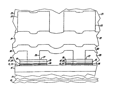
Figures lA and 1B represent a plan view of a portion of a monolithic
integrated circuit structure embodying the present invention and a layer
diagram of
a part of this structure,
Figure 2 represents a fragmentary portion of the layer diagram of
Figure 1B,
Figures 3A and 3B represent a plan view of a portion of a
monolithic integrated circuit structure embodying an alternative to the
invention
and the layer diagram of a part of this structure shown in Figures 1 A and 1
B,
Figure 4 represents a characteristic diagram for structures similar to
one of those shown in Figures lA, 1B and 2,
Figures SA and SB represent a plan view of a structure from Figures
lA, IB and 2, and an approximation thereof,
Figure 6 represents a graph of responses for a structure similar to one
of those shown in Figures lA, 1B and 2,
Figures 7A and 7B show graphs of characteristics for a structure
similar to one of those shown in Figures lA, 1B and 2,
Figures 8A and 8B are a circuit schematic diagram of a portion of
a digital memory system based on the structure shown in Figures lA, 1B and 2,
and
an equivalent circuit of a portion of that circuit schematic diagram,
Figures 9A and 9B are a circuit schematic diagram of a portion of
an alternative digital memory system based on the structure shown in Figures 1
A,
1B and 2, and a layer diagram showing additional structure to that shown in
Figures
1 A, 1 B and 2,
CA 02269539 1999-03-30
WO 98I20496 PCT/US97/20373
-11-
Figures 10A and 10B are a circuit schematic diagram of a portion
of an alternative digital memory system based on a structure partly similar to
that
shown in Figures lA, 1B and 2, and a layer diagram showing that structure, and
Figures 11A, 11B and 11C are circuit schematic diagrams of a
portion of alternative digital memory systems based on the structure shown in
Figures lA) 1B and 2.
DETAILED DESCRIPTION OF THE PREFERRED EMBODIMENTS
A digital data bit storage and retrieval memory cell suited for
fabrication with submicron dimensions can be fabricated that provides rapid
retrievals of bit data stored therein and low power dissipation by
substituting an
electrical insulator for a conductor in the nonmagnetic layer. This memory
cell can
be fabricated using ferromagnetic thin-film materials of similar or different
kinds
in each of the magnetic memory films used in a "sandwich" structure on either
side
of an intermediate nonmagnetic layer which ferromagnetic films may be
composite
films, but this intermediate nonmagnetic layer conducts electrical current
therethrough based primarily on a Quantum electrodynamic effect "tunneling"
current.
This "tunneling" current has a magnitude dependence on the angle
between the magnetization vectors in each of the ferromagnetic layers on
either side
of the intermediate layer due to the transmission barrier provided by this
intermediate layer depending on the degree of matching of the spin
polarizations of
the electrons tunneling therethrough with the spin polarizations of the
conduction
electrons in the ferromagnetic layers which are set by their magnetization
directions
to provide a "magnetic valve effect". Such an effect results in an effective
resistance or conductance characterizing this intermediate layer with respect
to the
"tunneling" current therethrough. In addition, shape anisotropy is used in
such a
cell to provide different magnetization switching thresholds in the two
ferromagnetic layers by forming one of the ferromagnetic layers to be thicker
than
the other. Such devices may be provided on a surface of a monolithic
integrated
CA 02269539 1999-03-30
WO 98l20496 PCT/US97/20373
- 12-
circuit to thereby allow providing convenient electrical connections between
each
such memory cell device and the operating circuitry therefor.
A "sandwich" structure for such a memory cell, based on having an
intermediate thin Layer of a nonmagnetic, dielectric separating material with
two
major surfaces on each of which a anisotropic ferromagnetic thin-film is
positioned,
exhibits the "magnetic valve effect" if the materials for the ferromagnetic
thin-films
and the intermediate layers are properly selected and have sufficiently small
thicknesses. The resulting "magnetic valve effect" can yield a response which
can
be several times in magnitude greater than that due to the "giant
magnetoresistive
effect" in a similar sized cell structure.
Figure lA shows a plan view of an example of such memory cells
as part of a digital memory formed as a portion of a monolithic integrated
circuit)
including a supporting semiconductor chip as part of the memory substrate)
which
can have conveniently provided therein the operating circuitry for this
memory.
Figure 1B provides a fragmentary view of a portion of the view shown in Figure
1 A
to show the layered structure thereof, and also has parts thereof broken out
to show
some of the structure therebelow) again for greater clarity. The protective
layer
provided over portions of the structure shown in Figure 1 A in actual use has
been
omitted in this view for clarity, but that layer is shown in part in Figure 1
B . Certain
other portions of some layers have been omitted, again for clarity, so that
the
structure portions present are shown in solid line form if they are exposed in
the
absence of some layer thereover now omitted, but with other structure portions
beneath the solid line form portions appearing in these figures being shown in
dashed line form.
Corresponding to Figures lA and iB is Figure 2 which is a layer
diagram of a corresponding portion of the structures shown in Figures lA and
1B.
this layer diagram gives an indication of the structural layers leading to
portions of
the structures shown in Figures 1 A and 1 B, but Figures 1 B and 2 are not
true cross
CA 02269539 1999-03-30
WO 98l20496 PCTIUS97/20373
-13-
section views in that many dimensions therein are exaggerated or reduced for
purposes of clarity.
As indicated above) the memory cell structures in these figures are
typically provided on a semiconductor chip, 10) having suitable operating
circuitry
for the memory provided in the resulting monolithic integrated circuit
structure. An
electrical insulating layer, 11, formed on semiconductor chip 10 by a sputter
deposition of silicon nitride, supports the memory cell "sandwich" structures
thereon each of which comprises a pair of ferromagnetic thin-f lm layers that
are
separated from one another by a nonmagnetic, electrically nonconductive or
dielectric intermediate layer, or barrier layer, as will be described in more
detail
below. A portion of just layer 11 is shown in the high resolution drawing of
Figure
2. Typically, layer 11 is formed by this silicon nitride deposited to a
thickness of
about 10,000. Photoresist is spread over layer 1 l and patterned to provide
via
openings therethrough and through appropriate ones of the insulating layers in
1 S integrated circuit 10.
A first interconnection, 11', for the above indicated memory cell
"sandwich" structures is next provided on insulating layer 11 as both this
interconnection and as a further substrate portion for supporting the memory
cell
"sandwich" structures to be subsequently provided. Thus, a metal deposition is
made on layer 11 of aluminum alloyed with 2% copper to cover that layer and
fill
the via openings therein for electrical interconnections to the integrated
circuitry in
and on the semiconductor substrate below. This metal layer is typically
deposited
to a thickness of 1000 ~. Photoresist is then spread thereover with openings
therein
where the unwanted portions of that metal layer are to be eliminated, and
reactive
ion etching is undertaken to provide this elimination of unwanted metal layer
portions. Interconnection and support structure 11' resulting from this
elimination
is shown in Figures 1B and 2.
Thereafter) the "sandwich" structures just mentioned are provided
on interconnection support layer 11 ' with each of the ferromagnetic thin-film
layers
CA 02269539 1999-03-30
W4 98I20496 PCT/US97/20373
-14-
and the intermediate layer being provided, or at least initially provided,
through
sputter deposition as a basis for forming a magnetoresistive memory cell. This
multilayer structure will have a vertical direction effective resistivity
based on the
quantum electrodynamic effect tunneling current passing therethrough which
might
range from 0.01 to 10,000 MSS-~tm2 because of the extreme sensitivity of this
effective resistivity to the thickness of the barrier layer. In addition, the
structure
will typically exhibit an effective capacitance and a magnetically controlled
tunneling effect response exceeding 20% between the minimum effective
resistance
value and the maximum effective resistance value achievable under such
control.
i0
In this structure, the first layer provided is a composite ferromagnetic
thin-film layer sputter deposited onto interconnection and support 11' with
the
result shown in Figure 2. A first stratum, 12, of this composite ferromagnetic
thin-
film layer is formed of an alloy of 65% nickel) 15% iron and 20% cobalt
deposited
to a thickness of 40~, which has a magnetic saturation induction of typically
about
10,000 Gauss, and this process results in the deposited film having a face-
centered
cubic structure. The deposition of this layer occurs in the presence of an
external
magnetic field in the plane of the film oriented along a direction parallel to
the
extended direction of interconnection and support I1' in Figure 1B This
fabrication magnetic field will leave the easy axis of the film similarly
directed.
Alternatively) the deposition field may be provided at an angle to the
extended
direction of interconnection and support I 1' to provide a bias rotation of
the layer
magnetization to facilitate switching the direction of that magnetization.
A second stratum, 13, is also provided in a sputter deposition step
2S in the presence of a similar fabrication magnetic field. Second stratum 13
is formed
of 5% iron and 95% cobalt to a thickness of 15A resulting in this material
having
a magnetic saturation induction of approximately l6,000 Gauss which is a
higher
value than that of the magnetic saturation induction of first stratum 12. This
higher
saturation material is provided adjacent the intermediate or barrier layer,
which is
CA 02269539 1999-03-30
WO 98I20496 PCT/LTS97I20373
-15-
the next layer to be formed, to thereby obtain a greater magnetically
controlled
tunneling effect, but the lower saturation value in stratum 12 is provided to
keep the
composite film more sensitive to smaller fields than it would be in its
absence. This
composite layer is designated 12) 13 in Figure 1B.
Thereafter, an intermediate or barrier layer, 14, is provided by
sputter deposition and oxidation onto layer 13, this intermediate layer being
a
dielectric. Layer 14 is begun typically by sputter depositing 12~ of aluminum
onto
layer 13, and continuing to provide two further angstroms of this material
using the
aluminum sputtering target but also introducing oxygen into the sputtering
chamber.
The result is to convert the already deposited aluminum layer substantially
into
aluminum oxide which expands its thickness by a factor of about 1.3, and to
add
another two angstroms of aluminum oxide thereto giving an intermediate layer
or
burner layer thickness of approximately 17.5 with the layer being formed
primarily of aluminum oxide. Any portion of the previously deposited aluminum
metal unoxidized in this process will result in a very thin layer of that
aluminum on
and between ferromagnetic layer 12,13 and the aluminum oxide dielectric
barrier
layer which can be advantageous.
The provision of layer 14 is followed by providing a second
composite fen omagnetic thin-film layer that is provided on layer 14, and its
structure matches that of the first composite ferromagnetic layer comprising
strata
12 and 13, except for being thinner and reversed in strata order, because of
the use
of essentially the same deposition steps. As a result) the stratum having the
greater
magnetic saturation induction is again adjacent to layer 14 in the second
composite
layer, and the lesser magnetic saturation induction stratum is provided
thereon but
with a thickness of only 25~. Since the strata are otherwise the same, they
have
been designated in Figure 2 as 13 ' and 12' in correspondence to strata 13 and
12.
After completing this "sandwich" structure, a 2000 layer of
tantalum or tantalum nitride is sputter deposited on stratum 12' to passivate
to
protect stratum 12' therebelow) and to allow electrical connections thereto
for
CA 02269539 1999-03-30
WO 98I20496 PCT/US97120373
- 16-
circuit purposes. The resulting layer, 15, is shown in broken form in Figure 2
because of its significantly greater thickness compared to the ferromagnetic
composite layers and the nonmagnetic intermediate or barrier layer.
Similarly, a further layer, 16, is deposited on layer 15, and is shown
in broken from in Figure 2 because of its relatively greater thickness of 100.
Layer 15 is first sputter cleaned which removes around 75~ thereof. Then)
layer I6
is sputter deposited on cleaned layer 15 as a chrome silicon layer with 40%
chrome
and 60% silicon to serve as an etch stop for the subsequent etching of a layer
to be
provided thereover as a milling mask.
That is, another layer of silicon nitride is next sputter deposited on
layer 16 to a depth of 1000A to be used as a milling mask, but this layer is
not
shown in Figure 2 because its remnants will be incorporated in a further
insulating
layer to be provided later. On this silicon nitride mask Iayer, photoresist is
deposited and patterned in such a way as to form a pattern for an etching mask
which is to be formed following that pattern by leaving the mask portions of
the
silicon nitride layer therebelow after etching. This last masking pattern in
the
silicon nitride is to result) after milling therethrough to remove the exposed
ferromagnetic and nonmagnetic layers therebelow) in a substantial number of
separated bit structures to serve as the memory cells in the digital memory
each
with a "sandwich" construction. Reactive ion etching is used with the
patterned
photoresist to remove the exposed portions of the silicon nitride masking
layer
down to chrome silicon layer 16 serving as an etch stop. The remaining
portions
of the silicon nitride layer protected by the photoresist serve as the above
mentioned
milling mask for the subsequent ion milling step which removes the exposed
portions of chrome silicon layer 16, and thereafter, also the then exposed
portions
of layer 15, the next exposed portions of the second composite ferromagnetic
thin-
film layer formed as strata 13' and 12', the subsequently exposed portions of
intermediate nonmagnetic layer 14' and, finally, the resultingly exposed
portions
CA 02269539 1999-03-30
WO 98/20496 PCT/LTS97/20373
-17-
of the first composite ferromagnetic thin-film layer formed as strata 13 and
12 down
to interconnection and support 11'.
A portion of one of the resulting memory cells, 17, from Figure lA
is shown in Figure 2) as indicated above, and has counterparts thereof shown
in
Figure 1B (where they are designated again by numeral 17) with only some of
the
layers in each such cell being represented as distinct in this latter figure.
The full
multilayer structure that is shown in Figure 2 with the distinct strata in the
composite ferromagnetic layers is not shown in that manner in Figure 1B
because
of the larger scale used in that figure. Some of these memory cells can also
be seen
in the plan view of Figure 1 A, and each of such structures is also designated
by
numeral 17 in that figure. The easy axes of the ferromagnetic thin-film
composite
layers in each of memory cells I7 are parallel to the direction of the longest
extent
of those structures. Each memory cell I7 is formed with a rectangular central
portion in this plan view continuing into triangular portions tapering away
from
opposite ends of the rectangular portion along the easy axis to form the ends
of the
cell.
Following the completion of memory cell or bit structure 17, another
layer of silicon nitride is sputter deposited over those structures and the
exposed
portions of interconnection and support I 1' to a thickness of 7500 to form an
insulating layer) 19. Photoresist is provided over insulating layer 19 as an
etching
mask to provide via openings therethrough, and through silicon nitride layer
11 and
appropriates ones of insulating layers in integrated circuit 10.
On insulating Iayer 19) so prepared, a further metal deposition is
made, again of aluminum alloyed with 2% copper, to cover that layer and fill
the
via openings therein, and in silicon nitride layer 11 and the insulating
layers in
integrated circuit 10. This metal layer is typically deposited to a thickness
of
1000. Photoresist is spread thereover with openings therein where the unwanted
portions of that metal layer are to be eliminated, and reactive ion etching is
undertaken to provide this elinunation of unwanted metal layer portions. The
CA 02269539 1999-03-30
WO 98I20496 PCTIUS97120373
-18-
structures that result from this elimination is shown in Figure 1B) and in
Figure lA,
as a plurality of upper interconnections, 20, for interconnecting memory cell
structure 17 in parallel to one another in conjunction with interconnection
and
support 11'. As a result of the via openings in silicon nitride layer 11)
upper
interconnections 20 are also interconnected with electronic circuitry in the
integrated circuits in semiconductor substrate 10 therebelow.
The completion of upper interconnection structures 20 is followed
by depositing another layer of typically 7500 of silicon nitride thereover,
and over
the exposed po'ons of silicon nitride layer 20 to force a further insulating
layer, 21.
Photoresist is provided over insulating layer 21 as an etching mask to provide
via
openings therethrough, and through silicon nitride insulating layers 19 and 11
as
well as though appropriate ones of the insulating layers in integrated circuit
10.
On insulating layer 21, prepared in this manner, a further metal
deposition is made) again of aluminum alloyed with 2% copper, to cover that
layer
I S and fill the openings therein, and in silicon nitride layers 19 and 11 as
well as the
insulating layers in integrated circuit 10. This metal layer is typically
deposited to
a thickness of 3500. Photoresist is spread thereover with openings therein
where
the unwanted portions of that metal layer are to be eliminated, and reactive
ion
etching is undertaken to provide this elimination of unwanted metal layer
portions.
The structures that result from this elimination are shown in Figure 1B) and
in
Figure 1 A, as a plurality of word lines, 22, for the memory each positioned
across
insulating layer 21, upper interconnection structures 20) and insulating layer
19
from corresponding memory cell structures 17 supported on and interconnected
to
interconnections and supports 11'. As a result of the via openings, these word
lines
are also interconnected with electronic circuitry in the integrated circuits
in
semiconductor substrate 10 therebelow. A further insulator layer) 23, is
provided
by sputter depositing 7500 of silicon nitride over word lines 22 and the
exposed
portions of insulator 21. Insulator 23 serves as a passivation and protection
layer
CA 02269539 1999-03-30
WO 98l20496 PCT/US97I20373
- 19-
for the device structure therebelow. Layer 23 is seen in Figure 1B but is not
shown
in Figure lA to avoid obscuring that figure.
A memory cell or bit structure 17 of the structure described resulting
from the just described process for fabricating same will have a relatively
linear
change in the quantum electrodynamic effect "tunneling" current therethrough
from
one ferromagnetic layer to the other with respect to the voltage provided
across the
cell, i.e. between these ferromagnetic layers, for relatively lower voltages
but the
current magnitude increases more than linearly for higher values of voltage
across
the cell. As the voltage across the cell increases, the fractional change in
the in the
"tunneling" current through the cell, for the ferromagnetic layers having
magnetizations changing from parallel to one another to antiparallel,
decreases to
being only half as great with several hundred millivolts across the cell as
occurs in
the situation with a hundred or less millivolts across the cell so that this
fractional
change with cell voltage will range from a few percent to 20% or more. The
fractional change in the resistance of the cell for the ferromagnetic layers
having
magnetizations changing from parallel to one another to antiparallel increases
to
about one and one-half the room temperature values when the cell is cooled to
77 ~
K, but the "tunneling" current through the cell increases by only about 10% to
20%
indicating that the effective resistivity of the cell is relatively
insensitive to
temperature (around 500 to1000 ppm/~C).
The effective resistivity of a cell 17 is set by the amount of
"tunneling" current through the cell permitted by barrier layer 14 for the
voltage
across the cell. The high sensitivity of the "tunneling" current to the
thickness of
the barrier layer leads to a wide range of cell resisdvities which have been
observed
to be from 0.01 to 1000 M~ - ~rm2. On the other hand, harrier layer 14 appears
to
permit relatively little magnetic coupling between the ferromagnetic layers
thereacross with the coupling fields typically being only a few Oe.
One structural arrangement alternative to that shown in Figure 1 that
is possible is shown in Figures 3A and 3B. In this alternative, the word
lines, now
CA 02269539 1999-03-30
WO 98l20496 PCT/US97120373
-20-
designated 22', are deposited directly on silicon nitride layer 11 with an
insulating
layer, now designated 23', deposited thereover to provide the supporting
substrate
for interconnection and support 11' and memory cells 17. Memory cells I7 are
again connected parallel using interconnection and support 1 i' on the lower
side
thereof and upper interconnection 20 on the upper side thereof to provide the
interconnections with memory cells 17 if connected in parallel therebetween.
Insulating layer 21 now becomes the protective and passivating layer for the
device.
A further alternative, not shown) would be to provide word lines above and
below
memory cells or bit structures 17 at some angle with respect to each other,
typically
at right angles, for providing magnetic fields to affect the corresponding
cell
provided between each crossover of such word lines so that current for this
purpose
need not be carned in interconnection and support 11'.
The fabrication steps just described are) of course, applied to
semiconductor material wafers having many integrated circuit chips therein to
serve
as memory substrates so that many such digital memories can be fabricated
simultaneously in and on such wafers. Once alI memory cell structures 17 are
fabricated on each chip substrate) along with all of the associated
interconnection
structures and word line structures as protected by the final insulating
layer, the
wafers are then ready for wafer testing) for the separating of the individual
devices
into separate chips) and the housing of them in "packages".
The plan view of the shapes of bit structures 17, i.e. having a
rectangular center portion tapering into triangular end portions at opposite
ends
thereof, are not the only plan view geometrical shapes which can be used. An
alternative would be to form memory cell structure I7 with a plan view
geometry
following a parallelogram. There may be other alternative plan view shapes for
memory cell structures 17 which can improve the packing density of those
structures on an integrated circuit chip substrate.
A representation of a pair of typical magnetoresistance
characteristics of a memory cell or bit structure 17 versus external magnetic
fields
CA 02269539 1999-03-30
WO 98I20496 PCT/LTS97l20373
-21 -
applied along its length, i.e. along its easy axis, is shown in Figure 4 for
an
individual bit structure example of relatively larger size rather than a
smaller
structure taken from a parallel string thereof as a more easily understood
example.
A fixed quantum effect tunneling a curnent of 2.OpA is used as the operating
current
through the device between the upper interconnection and the lower
interconnection
to that device. This known current, along with the measured voltage across the
cell,
provides the resistance of that cell.
The characteristic, 30, having the peak on the left in Figure 4
develops from initially having a sufficiently large magnetic field parallel to
the easy
axis (shown as a positive field on the plot) applied via current in the
adjacent word
line 22 and via interconnection and support 11' to force the magnetizations of
each
of the ferromagnetic thin-films 12, 13 and 13', 12' in the memory cell or bit
structure 17 to be oriented in the direction of the field. These
magnetizations will
thus be parallel to one another pointing in an initial common direction to
thereby
leave the electrical resistance of the cell at a minimum (here, approximately
31 k~2).
This initial condition is followed by continually reducing this field
toward zero and then reversing the field direction, after which the magnitude
of the
field is continually increased (shown as a negative field on the plot). As can
be
seen in the plot, this action begins to increase the resistance of the cell as
the
magnetization of thinner layer 13', 12' begins to rotate toward the opposite
direction to a greater degree than does the magnetization of thicker layer 12,
13.
This difference occurs because of the shape anisotropy which, as structure I7
becomes sufficiently small, dominates the material anisotropy induced by
deposition of the ferromagnetic layers thereof in a magnetic field or by layer
material choice or both.
As a result) these magnetizations begin to be directed more and more
away from one another as the field gets increasingly negative, thereby
increasing
the cell resistance, until the magnetization of the thinner layer is rotated
just past
90~ from the easy axis, whereupon it abruptly switches (at approximately -10
Oe)
CA 02269539 1999-03-30
WO 98I20496 PCT/L1S97/20373
-22-
to being significantly directed in the opposite direction from that of the
thicker layer
as it attempts to align with the fields provided by the word line and
interconnection
line currents. At that point, the resistance value correspondingly increases
abruptly
to the peak value shown of approximately 37 kf~. The switching field threshold
value is set by the bit width and the net magnetic moment of the ferromagnetic
layer
which in turn is set by magnitude of the saturation magnetization and the
volume
of that layer. Since the volume, and so the moment, can be chosen by selecting
a
suitable and different layer thickness with respect to that of the other Iayer
to
provide shape anisotropy) these ferromagnetic layers, even if otherwise
identical,
can have different switching threshold values.
As memory cells 17 are fabricated sufficiently small to be considered
as having the composite layer ferromagnetic thin-films used therein to be
single
magnetic domain structures, the critical magnetic field magnitude (-100e), or
threshold) for the thinner layer at which such switching occurs (a threshold
found
much like the well known Stoner Wohlfarth threshold which is defined for
larger
area films not subject to exchange coupling and edge effects) is determined
from
layer magnetic energy considerations including the magnitude of the magnetic
fields established by the interconnection structure current in addition to
that
established by the word line current. (The field due to the operating current
across
the intermediate layer can be neglected because this current is so relatively
small).
Further magnitude increases in the negative field do not, however, cause the
magnetization of the thicker layer to switch to being directed in the opposite
direction at the expected Stoner Wohlfarth threshold therefor because the
previous
switching of the magnetization direction of the thinner layer inhibits the
switching
of the magnetization of the thicker layer. The change in the direction of
magnetic
field occurring in the thicker layer due to the magnetization of the thinner
layer
coupled thereto, because of having been previously switched in direction, acts
against the switching of the magnetization of the thicker layer to effectively
increase its switching threshold.
CA 02269539 1999-03-30
WO 98I20496 PCT/US97/20373
-23-
The magnitude of the magnetic field in the thicker layer due to the
magnetization of the thinner layer (and vice versa) depends on the
demagnetization
fields in these layers) thus allowing, by selecting the interconnection
structure
current magnitude and the memory cell geometry to achieve an appropriate
demagnetization factor value, the setting of the degree of switching
inhibition. That
is, the width of the peak in characteristic 30 can effectively be set by the
cell design
in operating conditions. Once this elevated magnitude threshold value
(approximately -70 Oe) for the thicker layer is exceeded by the magnitude of
the
applied field to force its magnetization direction past 90~ from the easy
axis, the
magnetization of this layer also switches to result in the magnetizations of
the two
ferromagnetic thin-film layers again be oriented in a common direction
(although
opposite to the initial direction) to thereby sharply lower the resistance
value from
the peak value of approximately 37 lc~ to the relatively lower value of again
about
31 lcf~. Further increases in the magnutude of the negative field do not
significantly
further change the resistance value as the magnetization directions in each
layer are
forced slightly closer and closer to a common direction. Since the direction
of the
magnetization of thicker layer 12, 13 can only be switched by fields having
magnitudes greater than those that switch the magnetization direction of
thinner
layer 13', 12', the direction of magnetization of thicker layer 12, 13
effectively
determines the binary value, "0" or "1 ") of the data bits stored in the cell.
Hence) traversing this large portion of characteristic 30 shown in
Figure 4 by changing the externally applied magnetic field due to word line
current
from a relatively large positive magnitude to a relatively large negative
magnitude
in the presence of a sufficient interconnection structure current is
equivalent to
changing the magnetic state of both layers from pointing in one direction to
pointing in the apposite direction, i.e. to storing a new data bit by changing
the
previously stored data therein based on the direction of the magnetization
from its
initial direction and binary value to another direction and value. If the
initially
stored data bit value was the same as the new value to be stored, the
corresponding
CA 02269539 1999-03-30
WO 98I20496 PCTIUS97I20373
-24-
increase in the externally applied field magnitude in the opposite direction
to store
this new data bit, i.e. the increasing of the field in a positive direction
rather than
in the negative direction as described above, would not cause traversing the
peak
in characteristic 30 thus leaving the layer magnetization's direction and the
data bit
value unchanged.
The remaining characteristic, 31) in Figure 4 develops just as did
characteristic 30 if started from where the development of characteristic 30
terminated as described above, that is) by applying a positively increasing
magnitude field in the presence of a sufficient interconnection structure
current
based field magnitude after the occurrence of a large magnitude negative
field.
Again, the peak in the cell resistance arises in this characteristic by first
encountering a threshold like and near to a Stoner Wohlfarth threshold for
switching thinner ferromagnetic layer 13') 12' (approximately 8 Oe) to
increase the
cell resistance from again about 31 kf ~ to around 37 kS~, and thereafter
encountering
the elevated magnitude threshold for switching thicker layer 12, 13
(approximately
58 Oe) to decrease the cell resistance back to about 31 kSa. Thus) storing a
data bit
of either a "0" or "I" binary value in a memory cell 17 having the
characteristics
shown in Figure 4, as represented by the orientation direction of the
magnetization
of thicker layer 12) 13 along its easy axis in the scheme just described,
requires the
application of a sufficient magnitude word line field in the corresponding
direction
along that axis in the presence of a sufficient magnitude interconnection and
support structure field.
Retrieving the stored data without disrupting the value of that data
is easily done in a memory cell or bit structure 17 having characteristics 30
and 31,
the current one of these characteristics that the cell resistance will follow
upon
application of interconnection support current and word line current based
fields
having been determined by the direction of orientation of the last external
field
applied to the cell sufficiently large to switch the magnetizations of both
cell
ferromagnetic thin-film layers in the presence of the chosen interconnection
and
CA 02269539 1999-03-30
WO 98I20496 PCT/US97120373
-25-
support line current. A limited externally applied field, the limit imposed by
limiting the corresponding word line current and possibly the interconnection
and
support line current in the presence of the interconnection and support line
current
chosen is initially provided having a value capable of placing the resistance
of the
cell at one of its peak values in either one or the other of characteristics
30 and 3 I ,
and the cell structure voltage measuring circuitry may be concurrently
"autozeroed"
to thereby measure a zero value in these circumstances.
Such "autozeroing" circuitry and processing need not be used for a
single cell because of the relatively large signal change provided thereby)
but the
use of several such cells in parallel with one another in the circuit to which
the
voltage measuring circuitry is applied will reduce the output signal of a cell
because
of the parallel conduction paths to a value sufficiently small so as to
require
"autozeroing" if the individual cells in that circuit are not electrically
isolated from
one another such as by use of a switching arrangement or other electrical
isolating
means. Of course) the ability to dispense with the need to perform an
"autozeroing"
step and to eliminate the circuitry therefor can significantly increase the
information
retrieval rate in the memory cell circuit as well as allowing an increase in
the
density thereof in a monolithic integrated circuit chip. This initial field is
limited
in magnitude so as to be unable to switch the direction of magnetization of
thicker
layer 12) 13 in the presence of chosen interconnection and support line
current
magnitude.
To complete retrieving the stored cell information, the limited
externally applied field is then reversed from its initial direction to a
final limited
value in the opposite direction that is capable of placing the resistance of
the cell
at its other characteristic resistance peak, but riot capable of switching the
direction
of magnetization of thicker layer 12, 13 in the presence of the chosen
interconnection and support line current magnitude. If the cell resistance is
actually
at a resistance peak initially in following one of characteristics 30 or 31
because of
the direction of the last previously applied word line current base field of a
CA 02269539 1999-03-30
WO 98I20496 PCT/US97/20373
-26-
magnitude sufficient to switch magnetizations of both ferromagnetic layers,
the
resistance after the field reversal will decrease as the magnetization of the
thinner
layer switches to be oriented in the same direction as the direction of
magnetization
of the thicker layer. If the cell resistance is instead following the other
characteristics so that it exhibits a relatively low resistance initially) the
resistance
after the field reversal will increase as the magnetization of the thinner
layer
switched to be oriented in the direction opposite to the direction of the
magnetization of the thicker layer.
Thus) the resistance change on the reversal from a field oriented in
one direction of a magnitude limited to be at a resistance characteristic peak
to a
limited field oriented in the opposite direction will indicate which of the
characteristics 30 and 31 the cell followed, and so in what direction the last
sufficiently large externally applied magnetic field was oriented to thereby
indicate
the binary value of the data bit represented thereby. The change in the
resistance
value, 0R, is equal to the full change in resistance between the peak
resistance
value, representing the ferromagnetic layers magnetizations being opposed in
direction to one another, to the relatively low resistance value representing
the layer
magnetizations being oriented in the same direction as one another. This
retrieval
process provides a bipolar output indication since an increase of this
magnitude
indicates one stored data bit value and a decrease indicates the opposite
stored data
bit value. Thus, the difference between the magnetic state indication
representing
by an increase in resistance) +OR, and the magnetic state indication
represented by
a decrease in resistance, -AR, is + OR-(-OR) = 2~R, or twice the resistance
change
value to give the voltage measuring circuitry across the cell structure a
readily
detectable state differentiating output signal to measure from its "auto-
zeroed"
initial measuring point.
The rapidity at which such a binary data retrieval operation can be
performed in such a memory cell or bit structure 17 is initially limited by
the rise
time of the currents in interconnection and support 11' and in word line 22,
and by
CA 02269539 1999-03-30
WO 98I20496 PCT/US97I20373
-27-
the time required to rotate the magnetization vectors in the ferromagnetic
layers in
response to such a current. However) such a minimum data retrieval time limit
on the duration required to retrieve the data can be further lengthened by the
response time of the memory cell or bit structure 17 due to the capacitive
nature of
that cell in having a pair of ferromagnetic conductors on either side of a
dielectric
layer yielding an effective capacitance. An important parameter for memory
cell
or bit structure 17 is the intrinsic resistance-capacitance time constant of
the device
due to that barrier layer 14 resulting therein from the fabrication process of
the cell.
The cell capacitance) C) can be approximately determined for the cell from
C =8.8510-'8~8~IO~A /s
where A is the area in square microns and s is the thickness of the aluminum
oxide
portion of barrier layer i4 in microns and a dielectric constant of 8 has been
taken
as the value appropriate for the aluminum oxide of barrier layer 14. As
indicated
above, for relatively low voltages across the cell ( 100 mV or less), the
effective
resistance through the cell, R, will typically be on the order of 104 to 109
~. The
resistance of this portion of the barrier layer can be approximated by
R = k,sek2s
where k, and k2 are constants characterizing the barrier layer material and s
again
is the thickness of that layer in microns. As a result, the resistance-
capacitance time
constant which is the product of R and C will then be exponentially dependent
on
the thickness s of the aluminum oxide portion of barrier layer 14. This time
constant product can be reduced by reducing the thickness of the aluminum
oxide
portion of barrier layer 14 until k2s is much smaller than 1, or, as a
practical matter,
CA 02269539 1999-03-30
WO 98I20496 PCT/US97/20373
-28-
until difficulties in the fabrication process of thin barrier layers prevent
further
reductions in the thickness thereof.
A further lengthening in the minimum time to retrieve data from a
memory cell or bit structure 17 will be due to the voltage measuring circuitry
across
the cell involving a sensing amplifier to detect the change in the output
voltage of
that cell when the magnetizations of the ferromagnetic layer are changed from
parallel to one another to being antiparallel. Such a sensing amplifier will
have an
input resistance Ra typically equal to the combined resistances of the cells
connected thereto to provide approximately the maximum energy transfer from
the
cell to the amplifier.
If a single cell 17 is operated by a current source providing a current
value of I therethrough, the voltage across the cell will increase from I/Gm~
to a
value of 1/(G,~,~ 0G) where G",e,~ = 11R",;0 if an information retrieval
operation
results in the cell resistance going from R,~ to R~;a+~R. The effective
resistance-
capacitance time constant of the cell alone in an information retrieval output
circuit
having a matching input resistance to provide maximum energy transfer for this
increase in voltage forming the cell output signal voltage will be equal to
about
C/2G where C includes the capacitance of the cell as well as the input
capacitance
of the sensing amplifier. Alternatively, one may instead choose the amplifier
input
impedance to minimize the noise generated rather than to maximize the power
transfer and, as a result) increase the time constant by as much as two.
If the aluminum oxide portion of barrier layer 14 has a thickness of
2nm to give a value for C of approximately 0.035pF (ignoring the input
capacitance
of the sensing amplifier) from the above expression therefor, and the cell
exhibits
a resistance value from 104 to 109S2 for a cell having an area A of one square
micron
from the above expression therefor, the value of the resistance-capacitance
time
constant for the voltage rise on the cell through the sensed amplifier would
be
between 0.35ns and 35,OOOns. The need to be competitive with information
retrieval times of other kinds of random access memory requires that the
effective
CA 02269539 1999-03-30
WO 98I20496 PCT/US97I20373
-29-
resistance of a memory cell 17 be much closer to the value of I O~ fl then to
109 L2
to provide competitive data retrieval times) and so the aluminum oxide portion
of
barrier Iayer 14 must be sufficiently thin.
A further parameter to consider with a memory cell or bit structure
I7 is the associated electrical noise and its relationship to the available
signal
voltage change in switching the magnetizations of the ferromagnetic layers
therein
from anti-parallel to parallel. This signal voltage is, as can be seen from
the
foregoing) for a cell 17 with a fixed current therethrough that results in
approximately 100mV being dropped across the cell (the value of voltage above
which the response to a switching of the ferromagnetic layer magnetizations
decreases) will be the cell voltage response to the magnetization direction
switching
multiplied by 100 mV. If the ferromagnetic layer paralleling switching
response is
20%, the voltage change signal from the cell will be 20 mV. The noise voltage,
on
the other hand) is strongly related to the equivalent resistance R of the cell
and the
bandwidth, ~f) effective in the information retrieval output circuitry which
noise
voltage is known from electrical noise theory to at room temperature) be
V" = 1.2610-~oF,(Rmu'Of)sn)
where F is the noise factor of the voltage retrieval circuitry system having a
minimum value of unity. If the bandwidth ~f is taken to be 1001rHz, as is
typical
in random access memory data retrieval circuitry systems) the foregoing
expression
can be written as
V~ =1.26~lU~'F'Rm~~~l2
Clearly, the signal-to-noise ratio can be improved by making a
memory cell or bit structure 17 of larger area to give a lower resistance, and
therefore a lower noise voltage. For instance, a signal-to-noise ratio of 20,
which
is a value typically found sufficient for a random access memory to provide a
low
error rate, the above signal value of 20mV requires a noise voltage value for
V
which is less than 1mV for a noise factor value of the minimum value 1. This
CA 02269539 1999-03-30
W.O 98I20496 PCTIUS97/20373
-30-
requires that Rm;" have a value which is less than 890 kl;2. 1f the cell has a
resistivity
of 1000 t12-um2, a memory cell 17 would have to have an area of 1122 square
microns. On the other hand, a cell resistivity of 0.1 11S2-pmt would result in
a
memory cell needing to have an area of only 0.1 square microns. Again, the
aluminum oxide portion of barrier layer 14 must be thin enough to permit use
of a
memory cell having a sufficiently small area to result in a memory on a
monolithic
integrated circuit chip having a sufficiently high memory cell density.
As to the cell resistance versus applied external magnetic field
characteristics of a cell 17) magnetic structures are known, from
thermodynamic
considerations, to have stable equilibrium states of magnetization at minimums
of
the free energies of those structures. The total free energy of a bit
structure or
memory cell 17 can be given generally as
ETo~=E,+Ez+E,2.
where the total free energy is represented by E,.o~, the self-energy of the
first and
second layers is represented by E, and EZ, respectively, and the interaction
energy
between the two layers is represented by EIZ. As indicated above, a reasonable
approximation for the structure of a bit structure 17 is to assume that the
ferromagnetic thin-film layers therein are each of a single domain allowing
the
assumption that the magnetization of a layer changes only by rotation, and
that
these layers exhibit uniaxial anisotropy. These and further other reasonable
approximations, such as assuming there is no magnetic energy at present due to
magnetostriction or to other causes and that the operating current through
barrier
or intermediate layer 14 essentially perpendicular to the ferromagnetic films
provides a negligible magnetic field, allows an analytic representation of the
behavior of a bit structure or memory cell 17 that rather closely matches the
characteristics shown in Figure 4. The expressions provided for this purpose
representing these energies will be based on the bit structure shown in Figure
5A
as taken from bit structures 17 shown in Figures lA and 1B.
_.... _~.~ __..~.__._._. _-.._
CA 02269539 1999-03-30
WO 98J20496 PCT/US97J20373
-31-
The self-energy for this purpose of thicker ferromagnetic thin-film
composite layer I2) 13) designated here as the first layer, can be represented
as
2 2
E~ = H r~M siV~ sinz~6~ -6s~+ D~L~ siV~ sinz~9n+ D'""M s~Vi cosz~6y
+HwMs,V,cos{A,~ +HbM6,V,sin~8,~,
and the self energy of thinner ferromagnetic thin-film composite layer 13',
12'
considered the second layer can be similarly written as
2 2
Ez - HrzM szVz siriz~6z -93~+ Dz~M SzVz sinz{Az~'f' DzWM szVz cosz~9z~
+ H w M s2V~ COStl3? ~- H bM szVz sin~9z ~.
The first term in each of these self-energy expressions represents the
anisotropy
energy in the corresponding one of the layers due to the anisotropies present
therein,
primarily the anisotropy brought about by the deposition of these
ferromagnetic
films in the presence of a magnetic field leading to requiring energy to
deviate the
magnetization of the film from the easy axis therein established by such
deposition.
The effects of such anisotropies are cumulatively represented in a well known
manner by an effective anisotropy field in each layer) Hk, and H,~,
respectively,
multiplied by the saturation magnetization of that layer which is MS, for
layer 1 and
is MSz for layer 2. The angle between the magnetization of the first layer,
M~.
shown by a dashed line vector in Figure 5A, and the average easy axis is
CA 02269539 1999-03-30
W.O 98I20496 PCT/US97120373
-32-
represented by 8, . The angle between the magnetization of the second layer)
MZ,
shown by a solid line vector in that figure, and the average easy axis is
represented
by 6z. The volume of each layer, V~ for layer 1 and VZ for layer 2) multiply
the
respective terms to give the total anisotropy energy in each corresponding
layer. To
provide an initial rotation bias for the magnetizations in the opposite
directions in
the two ferromagnetic layers, the easy axis of each layer is rotated on angle
65
during fabrication. Such a bias reduces switching thresholds in cells 17.
The second and third terms in each of the last two energy
expressions represent the demagnetization self-energy for each of the
corresponding
layers in a form typically written therefor. In these terms, the symbols Dl~
and D2L
each represent the demagnetization factor corresponding to the length axis for
the
pertinent one of the first and second ferromagnetic thin-film layers in bit
structure
17. The symbols D, W and DZw in these terms each represent the demagnetization
factors corresponding to the width axis for the related layer.
The fourth terms of each of these expressions represent the energy
of the magnetization in the corresponding layer due to the current applied in
the
associated word line 22 to generate a magnetic field, Hw, shown directed from
right
to left in Figure 5A. Should a meander word line be used, the field
contribution
from current in that line would be merely added to, and part of, the field HW
supplied by the current through word line 22 over the corresponding bit
structure
I 7.
The last term in each of these expressions represents the energy of
the magnetization in the corresponding layer due to an effective bias current
being
also carned in upper interconnection 20 (which could be instead carried in
interconnection and support 11') as described above if any, this field being
designated by Hb and represented in Figure 5A by an upward pointing solid line
arrow assuming current flow in that bias line is from left to right. Such a
bias field
can used to aid in switching the direction of magnetization of the thicker
ferromagnetic layer.
CA 02269539 1999-03-30
WO 98I20496 PCT/US97/20373
-33-
The interaction energy between the two ferromagnetic thin-film
layers in a bit structure or memory cell 17 is given by
E l2 '- ~H a Vavg M a-avg COS(8, + V Z
V D +V D
zw 2 z ~W M 6~M az sin(8,~sin(8z~
V D +V D
+ ' a~ 2 2 tL M a~ M az cos(A, )cos(6z ~.
The first term in this interaction energy expression accounts for the exchange
coupling energy and the correlated surface waviness (textural variation)
coupling
energy which is represented by an effective exchange field, H~, in the usual
manner
to cover these couplings between the ferromagnetic thin-film layers. This term
is
multiplied by the average volume and magnetization of both of these layers, or
V,+Vz
V avB =
and
MS,T,+MSzTz
M s_e~g = TI + Tz ,
The last two terms in the ferromagnetic layer interaction energy
expression represent the effects of the magnetization in one layer upon the
magnetization in the other analogous to the well known dipole-dipole
interaction
through considering the magnetization in each layer as a dipole interacting
with the
magnetization in the other. Because of the extremely close proximity of the
two
ferromagnetic layers) the effective field in one layer due to the
demagnetization
CA 02269539 1999-03-30
WO 98I20496 PCTIUS97/20373
-34-
field in the other is taken to be identical to that source demagnetization
field,
ignoring any effects of the separation. These terms are responsible for the
switching inhibition described above (and some rotation aiding) leading to the
elevated magnitude threshold faced in switching the direction of magnetization
of
thicker ferromagnetic layer 12,13 when the magnetization of thinner layer 13')
12'
is directed oppositely to that of the thicker layer.
Ferromagnetic material masses of general shapes in a magnetic field
lead to very complex demagnetization factors characterizing the internal
response
of that mass to the field. Homogeneous bodies having surfaces characterizable
by
expressions in the second degree lead to demagnetization factors in uniform
fields
which are much more tractable) i.e. the magnetization factors for ellipsoids
have
been determined in analytical closed form. As can be seen in Figure SB, an
ellipsoid can be provided with corresponding ones of its axes numerically
equal to
the length, width and thickness of the ferromagnetic thin-film layers in bit
structure
I7 of Figure SA. The resulting ellipsoid can be seen to rather closely
approximate
those layers in viewing Figures SA and SB together) at least for thinner
composite
ferromagnetic layer 13') I2' exposed in Figure SA. However, the length and
width
of thicker ferromagnetic composite thin-film layer 12,13 is the same as that
of layer
13') 12' and the thickness differences between the two layers are easily
accounted
for by the different dimensions of the third axis of the ellipsoids used to
represent
them to reflect the difference between the thicknesses of those layers. The
resulting
demagnetization factors are
4~tcos~~)cos(~,~ I l l
"' sin3 ~~ sin2 a~)~F~k''~n-E~k~~~n
and
CA 02269539 1999-03-30
WO 98l20496 PCT/US97120373
-35-
4n cos(~)cos(~2 ) ~F~k ) )
zc - sin3(~z)sinz~az)~. z~~2 E~k
for the demagnetization factors corresponding to the lengths of the ellipsoids
representing the two ferromagnetic thin-film layers of memory cell 17 in
Figure SA,
and
4ncos(~)cos~~,)
D'W sin3(~,)sinZ~a,~cos2(a,)
x E~k,,y)-cos2~a,)F(k~>y)-sin~(a,)sin(~,)cos(~,)
cos(~)
and
4~cos(~)cos(~Z)
sin 3 (~Z )sin 2 ~a2 )cos2 (a2 )
sin2(az)sin(~2)cos(~z)
x E(k2,~z)-cost{az~F~kz~~~~- cos(~)
for the demagnetization factors corresponding to the widths of these
ellipsoids for
these layers.
In these equations for the demagnetization factors, the various
trigonometric terms) cos(~)) cos(~x), and sin(ax)) are defined as
cos (~) = W 0 s ~ S 2 ~ ,
CA 02269539 1999-03-30
WO 98I20496 PCTIUS97I20373
-36-
cos (fix) = Lx 0 s ~x s 2 ,
and
2 2
1 L _ sin() n
sin (a )_ - =k 0_<a <-
Tx ~2 sin (~~
L
where L is the length of the ellipsoid, W is the width of the ellipsoid, and
TX
represents the thicknesses of either of the two approximating ellipsoids
through x
being set to either 1 or 2 to indicate the first or second layer. The
functions denoted
by F(k,~) fix) and E(k,~) fix) are elliptic integrals of the first kind and
the second kind,
Z O respectively, defined as
( _ '~ 1
x z
F'k ,~ ~- 0 1-kx sln2(W)
and
E~kx,~x)= 1-kxsin2(W)d4~
0
These expressions for the demagnetization factors can be further
simplified in several situations, including the present situation where the
length and
width are of comparable magnitudes but each are more than an order of
magnitude
greater than the thickness, i.e.
Lz W~Tx.
CA 02269539 1999-03-30
WO 98I20496 PCT/US97/20373
-37-
In this circumstance, the demagnetization factors can be expressed as
_s
_ 2 2
D,~ =4nT, {1 L ) KeZE' =4nT,FL
and
_ i z _
D ZL = 4nT2 (1 L ~ K eZE' = 4nT2FL
for the demagnetization factors corresponding to the lengths of the ellipsoids
representing the corresponding one of the two ferromagnetic layers, and
2
D,w = 4nT1 E' - (1 a )K = 4~T~FW
Le2(1-e2)z
and
s
D2W =4nT2 E'-{1-a )K =4nTZFW
Le2{1-e2)2
for the demagnetization factors corresponding to the widths of these
ellipsoids
representing those layers. In these last equations for the demagnetization
factors,
the symbol a is defined as
W2 z
E = 1- L2 .
The functions K and E' are complete elliptic integrals given as
CA 02269539 1999-03-30
WO 98l20496 PCT/ITS97/20373
-38-
n
z 1
0 1-ez sinz(yr) dW
and
_n
E~ = z 1-ez sinzdy~.
0
Using these last expressions for the demagnetization factors, the
above expressions for the energy components in the free energy of the bit
structures
17 of Figure 5A can be rewritten to in simplified form. The self energy of
ferromagnetic thin-film layer 12,13 becomes
2
E) - H k~M 5n sinz ~B,As~+ 4nT,F2M S~V~ sinz ~9n
+ 4~tT,FwM s,V~ cosz~9y
2
+ H WM S,V, cos~A,?
+ H bM S,V, sin~A, ~.
The expression for the self energy of layer 13',12' now is
2
Z - Hk2Ms2V2 Sln2{82 -8sl+4~T2F2MSzV2 sinz~62~
+ 47tT2FWMszVz cosz~9z~
2
to
+ H W M SzVz cos~9z
-HbMSzVzsin~Az}.
CA 02269539 1999-03-30
WO 98I20496 PCT/US97/20373
-39-
Finally, the interaction energy expression becomes
E 12 - H eVrvgM avg COS~81 + 82
Vl4tcT2Fw + V24nT,F~,1
- M 6,M52 sin~8,~sin~8z~
2
V, 4 nTz FL + V z 4 nTl FL
+ 2 M a1M sz cos~6, ~cos~62
or
E lz = -H eV.~gM .~g cos~8, + 8z
VITz + VZTI
- 2 4nFW M s,M bz sin~6, ~sin~62
VITz + VzIT
+ 2 4~tF~Ma,MSzcos~8l~cos~92~.
Some limitations must be satisfied by bit structures 17 to have them
behave during digital data storage and retrieval operations as desired. The
width
dimension W thereof is subject to at least two conditions which limit its
extent to
being less than certain values. As indicated above in describing the operating
process, the switching of the directions of the magnetizations of the layers
at certain
threshold values of the word line current based fields depends on the
magnitude of
the bias fields due to the bias current since these bias fields affect those
thresholds.
The ability of the fields generated by the bias currents to affect the
thresholds will
be diminished and eventually disappear or become negligible as the width
dimension of bit structure 17 become increasingly wide. This begins to occur
when
the width of the bit structure exceeds twice the curling length experienced in
that
CA 02269539 1999-03-30
WO 98I20496 PCT/US97120373
-40-
structure for the magnitude of the word line current based field used for
switching
the directions of the layer magnetizations.
The magnetizations of portions near the sides of a bit structure 17
are pinned there in a direction parallel to the sides to a greater extent than
those in
the interior of the structure because of demagnetization considerations. Thus,
as
the structure widens, the applied field will at some point switch the
magnetization
of the layers in the interior central portions thereof without having switched
the
magnetizations of the layer portions near the edges thereof. As a result, the
fields
due to the bias current, which are orthogonal in direction to those induced by
the
word line currents, tend to interact with the magnetizations of the
ferromagnetic
layers in two counteracting ways rather than in one supporting way. That is,
the
fields due to the bias current will cause torques on the magnetizations
already
rotated in the central interior portions in one direction, but cause torques
on the
magnetizadons at the edges in an opposite direction to thereby in effect
cancel out
the torques on the magnetizations. The intent is instead to have the torques
generated by the bias current fields act in a common direction to aid the
switching
of the magnetizations under the applied word line current fields. Hence, the
width
of bit structure 17 should be no greater than twice such curling lengths
occurring
therein from its sides inward. If the width of a bit structure 17 is less than
twice the
curling length's characteristic thereof, the magnetizations of the layers,
both in the
central interior portions and near the outer side portions thereof, rotate
together and
so are subject to torques from the field generated by the bias current in a
common
direction.
On the other hand, the bias current can be kept sufficiently small so
as not to be a significant factor in determining the magnetization direction
switching thresholds, particularly when a meander word line is used. In any
event,
suitable operation of bit structure 17 as described above requires that
demagnetizing fields be of sufficient magnitude to serve to inhibit the
switching of
the thicker ferromagnetic thin-film layer magnetization once the magnetization
of
CA 02269539 1999-03-30
WD 98I20496 PCT/US97/20373
-41 -
the thinner layer has already been oppositely directed as described above.
This
inhibition is due primarily to the demagnetizing field components that
parallel the
width dimension of bit structure 17 since these demagnetizing f elds will be
considerably greater in magnitude than those along the length of that
structure
given that the width has significantly smaller extent than does the length. To
assure
that the demagnetizing fields associated with the width are dominant with
respect
to the anisotropy fields occurring in the layers, a bit structure 17 is
required to have
a width sufficiently small to result in the width component demagnetization
field
being larger than the anisotropy field for the layer) or that Hdx,
representing the
demagnetization field along the widths) be greater than H,~ leading to
Hax =DxWM.x =4nTxFqMBx > Hkx.
This inequality then yields
H kx
F"' > 4 nTx M sx '
or
H kx
2 ~ 47tTxN1 sx
Le2~1-ez~
Since K and E~ do not vary much in value with decreasing values of e) the
ratia of
the width to the length must be kept sufficiently small such that the e2
factor in the
denominator on the left side of the inequality is small enough to make the
inequality hold for the choice of thickness of the corresponding ferromagnetic
layer
material chosen) this material having a particular anisotropy field H,~ and a
particular saturation magnetization Msx.
Aside from its effect on the ratio of width to length in the last
equality) there are no significant further linutations on the Length of a bit
structure
17 beyond practicality limitations. One such limitation is that the need to
provide
CA 02269539 1999-03-30
WO 98I20496 PCT/US97/20373
- 42 -
a fairly uniform word line current based magnetic field across a bit structure
17
requires that the word line be approximately as wide as that bit structure.
For a
desired magnitude of the field generated by the word line current, that
current
necessary to provide that field magnitude becomes proportional to the width of
the
word line) that is, equivalently, to the length of the bit structure 17. Thus,
there is
not only a desire to keep the bit length short to allow as many as possible to
be
provided in the digital memory to improve its density of storage, there is
also a
desire to keep the word line currents as small as possible to reduce the heat
dissipation in the monolithic integrated circuit which also, as just
indicated,
requires keeping the bit structure lengths relatively short.
A final limitation on bit structure 17 is related to the required
difference in thicknesses between thicker composite ferromagnetic thin-film
layer
12,13 and thinner layer 13',12'. An insufficient difference in thickness
between
these two layers in the face of high rate of applied magnetic field changes,
such as
results from the use of an abrupt change in current in the word lines to
generate
such field changes, can lead to switching the direction of magnetization in
both
layers concurrently even though just one of them was intended to be switched.
That
is) if the difference in thickness between the layers, and so the difference
in
magnetization therebetween, is not sufficiently large, the direction of
magnetization
in each of these layers will switch together even if the magnitude intended
for the
switching field is only slightly larger than the switching threshold value of
the
thinner layer should the change in that field be applied at a high enough
rate. Such
high rates of application will result from the typical changes in word line
current
values resulting from transistor switches being switched off and on which
often
result in the current change approximating a step function.
Since the behavior of the magnetization in the ferromagnetic layers
of a bit structure in response to a sharply changing magnetic field is of
present
concern, the equations of motion for the magnetizations in the ferromagnetic
layers
in response to changes in magnetic fields are pertinent. Suitable equations of
CA 02269539 1999-03-30
WO 98l20496 PCT/US97/20373
-43-
motion are found to relate the time rate of change of the magnetization to the
torque
applied to that magnetization by all of the magnetic fields present plus some
damping of that motion. A well known equation expressing this relationship,
based
on choosing a certain form of such damping, is the Gilbert equation or
S
d M =y~M xH~- a M x d M .
dt Ms dt
Here, the magnetization is shown as a vector, M , as is the total magnetic
field
applied to the magnetization) H . The symbol y is the gyromagnetic ratio, and
the symbol a is the damping constant which will be quite small, typically in
the
range of 0.02 to 0.04.
Expressing this vector equation in its components represented in
spherical coordinates results in the following coupled system of first order
differential equations (for ferromagnetic thin-films with magnetizations
constrained
by vertical demagnetizing fields to essentially lie in the plane of the
corresponding
film) yields
d a - 4nM slYl + IYIa
dt 1+a2 ~ M,(1+a2)
and
d ~ _ 4~M salYl ~' (Y~
'C.
dt 1+az M5(1+a )
Here, 8 is the azimuthal angle (or ferromagnetic layer in-plane angle) and ~
is
the polar angle (or ferromagnetic layer out of plane angle) in spherical
coordinates.
The symbol t represents the torque effectively applied as a result of the
magnetic
fields present.
CA 02269539 1999-03-30
WO 98l20496 PCT/US97/20373
The response of the magnetizations of the thinner and thicker
ferromagnetic thin-films in a bit structure 17 to the dynamic application of
torques
via the magnetic fields generated by the associated word line currents can be
found
from these latter equations. Figure 6 shows a graph of the rotational angular
responses of the magnetizations to a word line current generated torque
shifting
abruptly from zero to a value of about 30 Oe. The lower coercivity thinner
layer
13') 12' is represented by an upper plot) 40, on that graph showing how it is
more
responsive to the applied torque than is the higher coercivity, thicker layer
12,13
represented by the lower plot designated 41. This upper plot is shown with the
thinner layer magnetization having rotated in response to an angle from the
easy
axis of about n radians, and so this plot reflects that the direction of the
magnetization is switched in that layer due to the application of the word
line
current generated field.
Notice that there is a substantial oscillation in the angular position
of this magnetization vector in reaching its final angular value as seen in
plot 40.
Although this oscillation, or "ringing") in the response of the magnetization
of the
thinner ferromagnetic layer to the step function in the word line field is
relatively
inconsequential to the operation of the device, a similar "ringing" occurs in
the
rotational angular behavior of the magnetization vector of the thicker layer
as seen
in plot 41 which can be of much more significance. The largest peak in the
"ringing" portion of the lower plot reaches an angular value that is more than
twice
the angular value of the final angular position taken by the thicker layer
magnetization as a result of the applied step function word line current
change and
the aiding effect of the magnetization angular position change in the thinner
layer
(up to the point of switching the magnetization direction in that layer).
Although not a problem for the bit structure represented in Figure
6 because the switching of the magnetization direction in the thinner layer
immediately thereafter begins to inhibit the angular positional change of the
magnetization of the thicker layer before it reaches ~t/2 radians) in some bit
CA 02269539 1999-03-30
WO 98I20496 PCT/US97/20373
-45-
structures having too small a difference between the thicknesses of the
ferromagnetic thin films or too small a sense current) or both) this initial
peak in the
"ringing" could reach the n/2 radian value. At that point) the thicker
ferromagnetic
layer switches the direction of its magnetization more or less concurrently
with the
switch in the direction of the magnetization of the thinner layer even though
the
ultimate final value intended for the angle of rotation of the magnetization
of the
thicker layer in response to the step function word line current change was
less than
n/2 radians. That is) a word line current step function could be applied with
the
intention of switching the direction of magnetization of the thinner
ferromagnetic
layer but not that of the thicker layer, but nevertheless result in switching
the
directions of magnetizations of both layers because of the peak in the
"ringing"
portion of the response of the magnetization of the thicker layer to the
applied field.
The implications of this dynamic behavior of the rotating
magnetizations of the thinner or thicker ferromagnetic thin-films in bit
structure 17
can be seen in Figures 7A and 7B. In these figures, the dynamic thresholds are
plotted as opposed to the quasi-static thresholds which result from minimizing
the
foregoing energy equations without regard to the dynamic behavior of the
structure
during operation. The quasi-static thresholds would be from 10% to 15% greater
than the dynamic switching thresholds shown in Figures 7A and 7B. These
switching thresholds are all found on the basis of using the highest rate of
change
in the effectively applied torque, that is) they are the thresholds which
result from
a step-function change in the word line current.
The lowest threshold, 50, represents the switching threshold for
thinner layer 13',12' when both the magnetization thereof, and of the thicker
layer)
have not yet been switched to a direction that is the same as the direction of
the
applied word line field. The next greater switching threshold, 51, is also for
the
thinner ferromagnetic thin-film layer, but with the thicker layer having its
direction
of magnetization matching that of the applied word line field. As can be seen,
the
magnetization of the thicker layer in this instance has inhibited the rotation
of the
CA 02269539 1999-03-30
WO 98I20496 PCT/CJS97120373
-46-
magnetization of the thinner layer to effectively raise the switching
threshold for
that thinner layer. In each instance, the thinner layer switching threshold is
plotted
as a function of the layer thickness difference but that layer has the same
thickness
of 401 for all the plots on this graph.
The next greateF switching threshold shown, 52, is the dynamic
threshold for thicker layer 12,13 when both this thicker layer and the thinner
layer
have the magnetizations thereof opposed to the direction of the applied word
line
field. As a result, there is no inhibiting effect from the magnetization of
the thin
layer on the magnetization change of the thicker layer so that both switch as
a result
of the applied field. However) switching threshold 52 is shown as a function
of
increasing thickness of the thicker layer to thereby result in an increasing
thickness
difference between the thicker and the thinner layer. Clearly, the switching
threshold increases significantly for the thicker layer as the difference of
thicknesses in the two layers increases. The final switching characteristic,
53,
represents the situation in which the thinner layer is already switched to be
directed
in the same direction as the applied word line field so as to inhibit the
switching of
the magnetization of the thicker layer. Again, switching characteristic 53 is
plotted
as a function of the increasing thickness difference between the layers.
As can be seen) the dynamic switching threshold plots for the thinner
layer cross the dynamic switching threshold plots for the thicker layer as the
thickness differences between the two layers sufficiently decrease. In this
situation,
there is clearly a substantial risk of having the directions of magnetization
in both
the thicker and thinner layer switch together in response to the application
of a step
function change in the word line current. As the thickness difference between
the
layers increases, an increasing gap develops between the switching thresholds
for
the thinner layer and the switching thresholds for the thicker layer thus
providing
a margin of safety in avoiding the switching of the thicker layer in response
to a
step-function change in the word line current intended to switch only the
direction
of the magnetization of the thinner layer.
CA 02269539 1999-03-30
WO 98I20496 PCT/US97/20373
-47-
Figure 7B shows dynamic switching thresholds of the same nature
as those shown in Figure 7A except they are found in connection with the use
of a
greater sense current, so in Figure 7B the threshold designation numerals
matching
those used in Figure 7A are followed by a prime mark to result in being
designated
51', 52') 53' and 54'. Switching thresholds in Figure 7B are established on
the
basis of an initial bias angle 8s_2 which, in effect) provides a field of 25
Oe in
opposite directions in each layer) as compared to the bias angle es_, used in
finding
the switching thresholds shown in Figure 7A where the effective field due
thereto
was only 15 Oe. Clearly, the use of a larger magnitude bias angle results in a
greater safety margin at lower thickness differences between the thinner layer
switching thresholds and the thicker layer switching thresholds.
Thus, the thickness difference between the ferromagnetic thin-films
used in a bit structure 17 must be sufficiently great, for the magnitude of
the bias
angle and the structure geometrical parameters used, to assure that the
application
of a word line field intended to switch the thinner layer does not also have
the effect
of an unintended switching of the thicker layer also. In many situations, the
thickness difference between the ferromagnetic thin-film layers will need to
exceed
at least 10~7o of the average of these two thicknesses.
The energy equations above, based on the ellipsoidal approximations
described there for bit structure 17 meeting the foregoing limitations, can be
minimized to find the equilibrium angular positions of the ferromagnetic layer
magnetizations as a function of the applied bias and word line current
generated
fields, and to find the quasi-static field thresholds. Necessary conditions
for such
an energy minimum are
2z = a E To, = o.
ae2
and
CA 02269539 1999-03-30
WO 98I20496 PCTIUS97/20373
-48-
a
~~ = ae~ ETo~ = o
Taking the derivative with respect to 61 to find the torque i, and
setting the result equal to zero as indicated in the equation for that torque
above
yields
~, = H ~, M ,, sin ~8, - 82 ~ co s~9, - 62
+ 4 nM E,T, ~FL - Fw ~V, sin~6, ~cos~A,
- H w M s, V, sin t9, ~ + H b M ,, V, co s~6,
+ H ~ T~~e T ~Y~ V' sin ~8, + 9z
v
-Tz4nF~,M B,M s2V,cos~A,~sin~6z~
- TZ 4 nF~M s, M s2 V, sin ~8 ) }cos~A2
=0
using Vx = ATx, with A being the surface area of the ferromagnetic layers, and
Ve~~
= ATeyg where the parameter TB~g is
T, + T2
Te~g = 2
S imilarly, the derivative with respect 62 of the total energy to provide the
torque z2
and setting it equal to zero as indicated above yields
CA 02269539 1999-03-30
WO 98I20496 PCTIUS97/20373
-49-
~2 - H t2M 5z sin(e2 -e2 )~OS~e~ -e2 ~
+ 4 nM 6zTz ~FL - FW ~Vz sin ~6z ~cos{8z
' H WM SzVz sin~6z~-H bM xzVz cos~9z~
+ H ~M a_a~gVz TT~B sin~9, + Az
2
-T,4nFWMa,MszVz sin~9,~cos~8z~
-T,4nF~M S,M SzVz cos~6,~sin~8z~
=0
A possibility for determining the equilibrium angles and the
switching thresholds is to use one of these torque equations to eliminate the
dependence in the total energy equation on either one of the magnetization
direction
rotational angles, and then find the second derivative of the energy and set
it to zero
to determine the point in which the system is going from a stable equilibrium
to an
unstable one) i.e. the switching point, yielding
2
d Etot~~x~
d a 2 = o.
x
Alternatively, the two torque equations can be solved self consistently to
obtain the
desired solutions. Furthermore, the resistance characteristics for the
corresponding
bit structure can be plotted versus applied word line current generated field
which
closely match those shown in Figures 3, 4A and 4B using these results and
CA 02269539 1999-03-30
WO 98I20496 PCT/US97/2,0373
-50-
R = R o + 4R sin e' $z
2
To determine whether such a resistance change has occurred as the
result of applying external magnetic fields to a memory cell, memory cells or
bit
structures 17 will be grouped for purposes of applying operating current
thereto for
information retrieval operations, and for connecting them to information
retrieval
output circuitry) to provide efficient use of surface areas in which such
cells and
such circuitry is provided in the monolithic integrated circuit structure.
Thus, a
succession of N memory cell or bit structure 17 could be connected in a series
string thereof, for instance, and supplied operating current of a magnitude I
flowing
through that series string to result in a voltage drop thereacross equal to
INRm;"
where R",;o is the minimum resistance of each cell absent applied external
magnetic
fields or at the extreme values of the external magnetic fields being used.
The
minimum resistance of each cell will be taken to equal that of all the others
for
simplicity.
A change in resistance of one selected cell in the series string
because of applied external fields of a magnitude sufficient to switch the
direction
of magnetization of the thinner ferromagnetic layer in that cell will be taken
to have
a value of DR in reaching its peak resistance value. Such an increase in
resistance
will result in an output signal of a magnitude equal to I(NRm;" + AR - NR~";"}
or SRI
which can be written IR~,;~~R/R",;" or IRm;or where r is the resistive
response ratio
of an individual cell, i.e. ~R/R",;o. In these circumstances, the signal-to-
noise ratio
of such a series string of memory cells) sln ~ s, can be written
_s _ IRmin~
n~s I.26~10'bF(NR,~;,)~~z
using the noise voltage found above for a single cell adapted for N such cells
in a
series string thereof. This series string of memory cells or bit structures I7
results
in a relatively large voltage being developed thereacross, INRm;~, for a
significant
__..... _,
CA 02269539 1999-03-30
WO 98I20496 PCTILTS97/203?3
-51 -
operating current I therethrough because of the high resistance of the barrier
or
intermediate layer 14 in each such cell, and the electrical noise in the
series string
increases with N'n so that the signal-to-noise ratio decreases by the factor
N''n.
Furthermore, the series string will have a relatively high impedance which the
information retrieval circuitry will have to match with its input impedance to
provide a maximum power transfer.
Monolithic integrated circuits are continually being operated at
lower and lower supply voltages, and therefore, may often be more compatible
with
a parallel interconnection of N memory cells or bit structures 17.
Furthermore)
limiting the voltage drop across each such cell to 100mV to obtain the maximum
fractional voltage response, as indicated above) is more easily done in a
parallel
connection of such cells than a series interconnection if there is substantial
resistance differences from one cell to another. Furthermore) the
interconnection
of cells in parallel reduces the effective impedance of the interconnected
string
which in some situations may be more compatible with the input impedance of
the
output information retrieval circuitry.
Such a parallel interconnected arrangement is shown in Figure 8A
Here, two sequences of memory cells or bit structures 17 out of an array of
many
are shown with the cells in each sequence being connected in parallel with one
another) an upper sequence which is connected to a first output information
retrieval circuit sensing amplifier, 60, and a lower sequence of parallelly
interconnected cells is connected to a further information retrieval output
circuit
sensing amplifier) 61. The two outputs of each of sensing amplifiers 60 and 61
provide complementary logic signals on a pair of data output lines, 62 and 63.
Sensing amplifier 60 is enabled by a first enable line) 64, and sensing
amplifier 61
is enabled by a second enable line, 65.
Each of memory cells or bit structures 17 in the upper sequence
thereof has a word line 22 passing by it, and each is connected between upper
interconnection 20 and interconnection and support 11'. In switching circuitry
not
CA 02269539 1999-03-30
WO 98l20496 PCT/US97/20373
-52-
seen, interconnection and support 11' and interconnection 20 can be connected
to
carry an operating current I of which a fraction is provided to each cell 17
connected therebetween during information retrieval processes while their
corresponding sensing amplifier is enabled, and while the word Iine adjacent
the
cell selected for retrieval has current directed therethrough sufficient to
switch the
magnetization direction of thinner ferromagnetic layer 12') 13' therein. For
information storage processes, interconnection and support I1' and the
corresponding one of word lines 22 can be switched to both have substantial
currents passed therethrough that together are sufficient to provide a
magnetic field
to switch the direction of magnetization of thicker layer 12, 13 in the
corresponding
one of cells 17.
Figure 8B shows a basic equivalent circuit for one of the
interconnected parallel sequences of memory or bit structures I7 depicted in
Figure
8A, the upper sequence being chosen for illustration in Figure 8B. Each of
cells 17
is represented by a resistance having a value of Rn,;o and a capacitance
having a
value of C. One of the cells 17, in addition to being represented as having a
resistance of R",;", has had its magnetic state changed so as to be further
represented
as exhibiting an additional resistance of value 0R above its minimum value of
R~;~.
Again for simplicity, a11 cells are represented as having the same resistance
and
capacitance values except for the one exhibiting the added resistance value of
OR.
Sense amplifier 60 is shown having an internal impedance represented by a
resistor
with a value of resistance Ra and a capacitance having a capacitance value of
Ca.
In this circuit arrangement for interconnecting a group of cells 17 to one
another
and the information retrieval output circuitry, the effective resistance-
capacitance
time constant would be with Ra = I/Ga
NC+C
NG~ax'+'C1a .
_.....r~.. t ....... ... ........
CA 02269539 1999-03-30
WO 98I20496 PCT/US97I20373
-53-
which) for small Ca and maximum energy transfer so that Ra = Rmin/N, again
becomes
NC _ C
N G mex + N G mex 2 G mex
The resistance of N parallel resistances of value R",;" is equal to
Rm;n/N. The resistance value of (N-1 ) resistors of value R,n;o in parallel
with each
other and in parallel with a further resistance of value R",;o+0R is
2
R min + R min~R
NRm;~ +(N -1)~R
As a result) the output signal of the sequence of memory cells 17 connected in
parallel when one of them has an increase in resistance of 0R is
z
1 R min + R mineR - R min
NRm;" +(N -1)DR N
This can instead be written as
DR
IR min R min _ IR min r
N N +(N -1) ~R N N +(N -I)r
R min
where r is again the response ratio ~R/R",;~.
If a voltage Vo of approximately IOOmV is to be nominally
maintained across each of memory cell I7 in the parallelly interconnected
sequence
thereof to keep them at their maximum output signal sensitivity, as indicated
above,
CA 02269539 1999-03-30
WO 98I20496 PCT/US97/20373
-54-
the nominal voltage drop across that interconnected array can be written as
V~ to give
~R
V R moo = V r
~ N +(N -1) ~R ~ N +(N -1)r
Thus, the output signal of the array of parallel interconnected memory cells
decreases as the number of memory cells increases, that is, the
magnetoresistive
response ratio r of an individual memory cell effectively is decreased as the
number
of memory cells in parallel increases giving an output signal that decreases
from
around 20 mV for an individual cell to around 2 mV if 10 such cells are
connected
together in parallel.
The signal-to-noise ratio of the array of parallel interconnected
memory cells becomes
I
s V~ N + (N -1)r
il2 '
1.2b' 10F R min
N
As can be seen, the electrical noise is reduced in the array of parallel
interconnected
memory cells by a factor of ( 1 /N) In due to the memory cells being connected
in
parallel which leads to a reduced effective resistance for the sequence as the
source
of electrical noise therein. This reduced noise, of course, is countered by
the
reduced value of the output signal so that the signal-to-noise ratio also
decreases
by the factor (N)-'n (actually, a bit more than that depending on the value of
the
response ratio).
CA 02269539 1999-03-30
WO 98I20496 PCT/US97/20373
-55-
Such circumstances will, in many instances, require finding some
other kind of circuit arrangement in which to interconnect a group of memory
cells
or bit structures 17 with information retrieval output circuitry which does
not lead
to reducing the signal at the output from a single cell 17 of around 20mV to
some
effectively much smaller signal value in the presence of a group of
interconnected
cells dependent on the number of cells so interconnected. One way of
preserving
this output signal value of around 20mV from each memory cell or bit structure
17
in an array thereof to the information retrieval output circuitry is shown in
Figure
9A. There, n-channel enhancement mode metal-oxide-semiconductor field-effect
transistors (MOSFET's), 70) are provided in and on semiconductor substrate 10
each in series with a corresponding one of memory cells or bit structures 17.
In
such an arrangement, these transistors are able to, when in the "off'
condition,
substantially electrically isolate the corresponding one of those cells from
the
corresponding conductor leading therefrom to the information retrieval output
circuitry) and so from the other cells in the group or array.
Each of transistors 70 has its source, 71) electrically connected
through an interconnection, 72, to a corresponding one of cells 17. Each of
transistors 70 has its drain, 73) electrically connected to a conductor, 74,
which in
turn is electrically connected to allow the switching thereof to an electrical
energization source, not shown) which supplies operating current to any
selected
one of cells 17 connected through its corresponding transistor 70 thereto.
Conductor 74 is also connected to a selection MOSFET, 75, serving as a pass
transistor which in turn is connected to sensing amplifier 60. Each of
selection
transistors 75 is switched into the "on" condition by a corresponding signal
on the
corresponding one of the gate selection interconnections, 76, connected to its
gate.
The opposite side of each of cell 17 is electrically connected through
an interconnection, ?7, to a further conductor) 78, which in turn is
electrically
connected to allow the switching thereof to an electrical energization source,
not
shown, which either draws operating current from any selected one of cells 17
CA 02269539 1999-03-30
WO 98I20496 PCT/US97I20373
-56-
connected thereto, or supplies a magnetic field generating current for aiding
in the
switching of the magnetization direction of a ferromagnetic layer or layers in
a cell
17. In the latter instance) the magnetic field generated by a current in
conductor 77
can aid the magnetic field generated by current in a word line 22 passing near
one
of cells I7 of interest to have either or both magnetic fields available for
information retrieval or information storage purposes. Transistors 70 are
switched
between the "on" condition and the "off' condition by selection signals
applied to
their gates, 79, over corresponding conductors, 80.
Transistors 70 can alternatively each be interchanged in position
with its corresponding cell 17 in the series connection thereof between a
conductor
74 and a conductor 78 to place that cell in the transistor drain circuit
rather than its
source circuit without significant effect on the electrical isolation of the
cell from
other cells. Also, bipolar transistors could alternatively be used for
transistors 70
rather than the MOSFET's shown. Of course, the implementing structures in
i 5 monolithic integrated circuits for these alternatives would require
substantial
changes from that used with the MOSFET devices shown.
Coincident currents are used for selecting a cell I7 as the basis for
retrieving information therefrom or for storing information therein. To
retrieve
information from a cell I7, a signal is provided over conductor 80 to gate 79
of the
transistor to which that cell is connected to switch that transistor into the
"on"
condition, and an electrical energization source is switched onto conductor 74
to
provide operating current through the transistor and the corresponding
selected cell
which is carried away on conductor 78. A current in the corresponding one of
word
lines 22 for that cell is generated sufficient to switch the magnetization of
the
thinner one of the ferromagnetic layers in the cell as part of the retrieval
operation
process. The switching on of transistor 70 allows a resistance shift in cell
17 to
cause an increased voltage drop thereacross which is sensed through that
transistor
70 on line 74 by sensing amplifier 60 which receives that signal through the
_.m... . T
CA 02269539 1999-03-30
W.O 98I20496 PCTIUS97120373
-57-
corresponding one of selection transistor 75 selected by a signal on the
corresponding one of selection line 76.
An information storage operation, on the other hand, requires
coincident currents being switched onto conductor 78 and word line 22 which
together provide a sufficiently large magnetic field to switch the
magnetization
direction of the thicker one of the ferromagnetic layers in the selected one
of cells
17 at which the currents are coincidentally presented. Transistors 70 are
switched
into the "off' condition during such storage operations.
One possible construction for a portion of a monolithic integrated
circuit chip to provide the circuit arrangement shown in Figure 9A is
indicated in
the layer diagram for one of cells I7 and the associated transistor 70 shown
in
Figure 9B. There, semiconductor material substrate 10 of p-type conductivity
has
transistor 70 formed in and on a portion of a major surface thereof which is
made
available by providing an opening in a device isolating field oxide, 81. Drain
73
and interconnection 74 are formed by an implanted n+-type conductivity region
in
semiconductor substrate 10, and separated from a similar n;-type conductivity
implanted region forming source 71 by doped polysilicon gate 79 extending to
doped polysilicon conductor 80 not seen in this figure. Gate 79 is separated
from
semiconductor substrate 10 by a thin gate oxide, 82. Transistor 70 as
described is
formed by well known techniques for the fabrication of such transistors in
monolithic integrated circuits.
A further insulating oxide layer) 83, has been provided over
transistor 70, and an opening has been provided therein over source 71 in and
over
which a first metal deposition is provided. This result is and subjected to a
planarization process to leave a metal plug of aluminum alloyed with 2% copper
as interconnection 72 extending through oxide layer 83 from source 71 to the
upper
surface of this oxide layer. On this metal plug, or interconnection, 72 is
formed a
memory cell or bit structure 17, in the manner described above. Using well
known
techniques following such a provision, a layer of silicon nitride, 84, has
been
CA 02269539 1999-03-30
WO 98l20496 PCT/US97/20373
-58-
deposited and then patterned to provide a opening therein to memory cell 17 in
which a second metal deposition and patterning has been provided to form
interconnection 77 and conductor 78) again an aluminum alloy with 2% copper.
Another layer of silicon nitride, 85) is then deposited as a base for the
subsequent
deposition of a metal layer to form word line 22, again of aluminum alloyed
with
2% copper. Finally, a passivating and protective layer of silicon nitride, 86,
is
deposited.
In an alternative cross-point interconnection arrangement for
information retrieval output circuitry interconnecting groups of cells 17,
coincident
currents are again used in both information retrieval operations undertaken to
retrieve information from those cells, and in information storage operations
used
in connection with such cells. Such a circuit arrangement is shown in Figure
10A
where conductors 74 are now connected directly to one side of the succession
of
memory cells or bit structures 17, and are connectable to an electrical
energization
source at one end thereof to provide either operating currents or a magnetic
field
generating current for those cells connected thereto. In addition) conductors
74 are
also connected to a corresponding one of pass transistors 75 as in Figure 9A
which
can each be switched into the "on" condition by signals provided on the
corresponding selection line 76 connected to its gate to thereby provide a
conductive path from the corresponding conductor 74 to sensing amplifier 60.
Conductors 78 are this time shown extending in a direction substantially
perpendicular to conductor 74, and they can carry away operating current from
a
selected cell 17 electrically connected thereto or can carry current to
generate a
magnetic field thereabout which will affect those cells 17 electrically
connected
thereto.
If cells 17 were each, directly connected to a corresponding
conductor 78, so as to each be directly connected between a corresponding one
of
conductors 74 and a corresponding one of conductors 78, the connecting of an
electrical energization source to a selected conductor 74 and a selected
conductor
CA 02269539 1999-03-30
WO 98I20496 PCT/tJS97120373
-59-
78 would lead to current in other current paths through the array beyond the
current
path through the cell 17 connected between these two selected conductors.
Current
in such other current paths can lead to undesirable effects with respect to
the output
signal from the intended selected cell directly connected between the selected
conductors. Such unwanted effects can again be alleviated by providing
sufficient
electrical isolation of each cell 17 from the other cells present in the array
so that
substantially the full 20mV output signal available from the selected cell
will reach
sensing amplifier 60 through the corresponding enabled one of transistors ?5.
One way this can be accomplished is shown in Figure 10A by
connecting a diode, 90, between each cell 17 and its connection to a
corresponding
conductor 78 with the diode anode connected through an interconnection, 91, to
cell 17. This prevents any conductive path portions extending from conductors
78
through corresponding cells 17 to the corresponding conductors 74.
Alternatively)
the positions of each of diodes 90 and its corresponding cell can be
interchanged
in the series connection between a conductor 74 and a conductor 78 without
significant effect on the electrical isolation of a cell from the other cells
in the
interconnected group, although a different structural implementation would be
used
in a monolithic integrated circuit. Thus) in this alternative) the cathode of
the diode
would be connected to its corresponding one of cells 17.
Figure 10B shows a portion of a layer diagram of one of cells 17 and
the corresponding diode of Figure 10A formed in a well known manner along with
the interconnections 74 and 78 extending substantially perpendicular to one
another
also formed by known techniques. Semiconductor substrate 10 of p-conductivity
first has a n''-type conductivity region, 92, implanted therein in an opening
in field
oxide 81 to prevent any transistor action occurring between substrate 10 and
the
regions to be subsequently provided in that substrate above region 92. This
region
is designated 92, 78 because it will also form part of conductor 78.
Thereafter, a
further n-type conductivity region, 93, is implanted through that same opening
in
oxide 81 over and into region 92 to complete the diode cathode and also again
form
CA 02269539 1999-03-30
W0 98/20496 PCT/US971~0373
-60-
part of conductor 7$. This is followed by implanting a p-type conductivity
region,
94, through the same oxide opening over and into region 93 to form the diode
anode. An oxide layer, 95, is then provided over this field oxide opening,
oxide
layer 81 and region 94, and an opening is thereafter provided in oxide layer
95 to
provide an access opening to region 94. A first metal layer of aluminum
alloyed
with 2% copper is then deposited and patterned to fill this opening to provide
a
metal plug, or interconnection) 91, with the result subjected to a
planarization
process. A memory cell or bit structure 17 is then formed on metal plug 91 in
the
manner described above.
Thereafter) using known techniques, a silicon nitride layer, 96, is
deposited over the exposed surfaces of metal plug 91) oxide layer 95 and cell
17.
An opening is provided in silicon nitride layer 96 to reach cell 17 and metal
is
deposited in a second metal deposition step) again aluminum alloyed with 2%
copper) to provide conductor 74 after patterning. A further passivating and
protective silicon nitride layer, 97, is then provided.
Small memories which are embedded in other circuitry being used
therewith often require larger output signals than are provided by memory
cells or
bit structures 17 directly. Such cells can be incorporated in a flip-flop
arrangement
to provide the current steering necessary to place the flip-flop in a selected
state.
Two such flip-flop circuits are shown in Figures 1 lA and 11B.
Figure 11A shows a pair of n-channel enhancement mode
MOSFET's, 100 and 101, each having its source electrically connected to a
ground
reference potential terminal, 102) provided in conjunction with a positive
voltage
power supply terminal, 103, suited for connection to a source of positive
voltage.
Each of transistors 100 and 101 has its drain connected to the source of a
corresponding one of a pair of n-channel enhancement mode MOSFET's, 104 and
105, serving as loads in the drain circuits of the corresponding ones of
transistors
100 and 101. Load transistors 104 and l05 each has its gate connected to its
drain.
These drains in turn are connected to positive supply voltage terminal 103.
CA 02269539 1999-03-30
WO 98l20496 PCT/US97120373
-61 -
The side of the circuit of Figure 11A having transistors 100 and 104
connected in series with one another, and the side of that circuit having
transistors
101 and 105 connected in series with one another, are cross-coupled to one
another
through use of two memory cells or bit structures 17. Each of cells I7 has one
side
thereof connected to a corresponding one of the drains of transistors 100 and
101,
and has the other side thereof connected to the gate of the opposite one of
those
transistors. In addition, a word line 22 extends past each of cells 17 but
carnes the
current therethrough in opposite directions by each of those cells so as to be
able
to switch the magnetization directions in the ferromagnetic layers of each
cell in a
direction opposite to that of the other. A further word line) 22', is also
provided
past of each of cells 17 so that cells 17 can be selected for magnetization
direction
changes of the thicker ferromagnetic layer therein through the use of
coincident
currents in word lines 22 and 22'.
Since of each cells I7 are in the opposite storage state in having the
magnetizations of the thicker layers therein pointing in opposite directions
with
respect to fields generated by currents in word line 22', a switching of
voltage from
the ground potential to a substantial positive level on positive voltage
supply
terminal 103 coincident with current through word line 22' will result in one
of
cells 17 being in the minimum resistance condition and the other in the
maximum
resistance condition. As a result, a greater current will pass through the
cell with
the smaller resistance into the parasitic capacitance extending to ground from
the
gate of the corresponding one of transistors 100 and 101 to which it is
connected.
This parasitic gate capacitance will thus gain charge more rapidly to thereby
switch
that transistor to the "on" condition, and so prevent the opposite one of
those
transistors from switching into that condition because of the decrease in the
drain
voltage of the "on" transistor to a value below the threshold voltage of the
opposite
transistor having its gate connected to this drain as this "on" transistor
draws
current through its load. The two different voltage levels at the drains of
transistors
100 and 101 after such a switching of sufficient positive voltage onto
terminal 103
CA 02269539 1999-03-30
WO 98l20496 PCT/US97/20373
-62-
represent the digital information and its complement stored in the thicker
ferromagnetic layers of the cells 17.
The flip-flop will maintain this condition for the positive voltage on
terminal 103 being maintained even after current is removed from word line 22'
since the voltage at the drain of that one of transistors 100 and 101 which is
switched into the "on" condition will continue to be of a value less than the
threshold voltage of the other. This output result of switching from ground
potential to a sufficient positive voltage on terminal 103 along with the
coincidental
provision of current in word line 22' can be changed for the next such
switching
only by having previously coincidentally provided word line currents through
word
line 22' and word line 22 to thereby have switched the magnetizations of the
thicker
one of the ferromagnetic layers in each of cells 17.
A similar operation is achieved in the complementary metal-oxide-
semiconductor field-effect transistor (CMOS) circuit of Figure 11B when the
voltage on positive supply voltage terminal 103 is increased from ground
potential
to a sufficient positive potential, but the dependence on the parasitic
capacitance
of the gates of transistors 100 and 101 is not as significant because of the
changed
configuration. Transistors 104 and 105 in Figure 11 A are replaced with a pair
of
p-channel enhancement mode transistors, 104' and 105') in Figure i 1B with the
gates thereof electrically connected to the corresponding gates of transistors
100
and 101, respectively. The gates of transistors 100 and 104' are cross-coupled
to
the other side of the circuit through being directly connected to the drain of
transistor 105') and the gates of transistors 101 and 105' are similarly cross-
coupled
by being directly connected to the drain of transistor 104'. Cells 17 are each
connected between the source of one of transistors 104' and 105' and the drain
of
the corresponding one of transistors 100 and 101.
Thus, as positive voltage is switched onto positive supply terminal
103 with a coincident current flowing in word line 22', the one of cells 17
having
the larger resistance will lead to a greater voltage drop across it and the
__ ___. ~ __. . ... ,
CA 02269539 1999-03-30
WO 98l20496 PCT1US97/20373
-63-
corresponding one of transistors 100 and 101 to the drain of which it is
connected
so as to switch into the "on" condition first the opposite one of those
transistors.
A temporary current will flow through this "on" condition transistor) the cell
17
connected to its drain and the p-channel transistor connected to that cell
with this
latter transistor than switching into the "off' condition. This will leave the
other
p-channel transistor in the "on" condition and the n-channel transistor in
series
therewith and the other cell 17 in the "ofF' condition. Again) this output
result of
switching from ground potential to a sufficient positive voltage on terminal
103
along with the coincidental provision of current in word line 22' can be
changed for
the next such switching only by having previously coincidentally provided word
line currents through word line 22' and word line 22 to thereby have switched
the
magnetizations of the thicker one of the ferromagnetic layers in each of cells
17.
The circuit shown in Figure 11C has the cells I7 repositioned from
the drain circuits of transistors 100 and 101, as shown in Figure 11B, to the
source
circuits of those transistors to each be connected between a corresponding one
of
those sources and ground. Much the same operation will occur for this circuit
as
the for the circuit in Figure 11B except that the one of cells 17 having the
larger
resistance leading to a greater voltage drop across it will prevent the one of
transistors 100 and 101 connected thereto from switching into the "on"
condition
first resulting in the other of those transistors doing so.
Although the present invention has been described with reference
to preferred embodiments, workers skilled in the art will recognize that
changes
may be made in form and detail without departing from the spirit and scope of
the
invention.