Note: Descriptions are shown in the official language in which they were submitted.
CA 02269620 1999-04-22
WO 98/20321 PCT/US97/20922
SCALABLE NON-CONTACT OPTICAL
BACKSCA1TER INSERTION PROBE
FIELD OF THE INVENTION
The present imrention relates to a non-contact optical bachscatter insertion
probe for
measiuing baclcscattaed light from a liquid, solid or gas medium. The measured
backscattered light
signal or spectral signature from a medium is analyzed to estimate the
constituents or chemical
composition of the medium. The probe is scalable in size for both large-scale
and small-scale
applications.
BACKGROUND OF THE INVENTION
There are mm~rous techniques for analyzing the chemical constituents of a
liquid mixture,
gas or solid medium by relating selected optical properties of a liquid or
other medium to the
constitutrts and their conce~ations within the modium. Many of these
techniques measure the
reflectance, scattering, transmittance or attenuation of electromagnetic
energy. Another technique
is to measure baclelectromagnetic energy (EME) from a medium in response to
light falling
on or ~tering the medium in a given direction The measm°emeats of
spectral signat<ues of a medium
are generally analyzed by application of algorittmos, mathematical models
and/or solutions of radiative
1
CA 02269620 1999-04-22
WO 98/20321 PCT/US97/20922
transfer theory. The ability to measure the backscattered light directly
enables scientists and
application engineers to utilize this signal to estimate constituents of a
medium more easily and
accurately, as well as to improve understanding of radioactive transfer
phenomena.
There are a number of laiown methods for measuring EME backscatter of a
medium. A few
ofthese methods are desalted in U.S. Pateut Nos. 3,990,795; 4,006,988;
4,226,540; 4,774,417; and
4,983,040. However, the known methods for measurement of EME backscattering do
not enable
measurement of the EME backscatter from a medium by using a probe of
relatively simple design
which is easy to construct, scalable for use in numerous applications,
corrosion-resistant, measures
EME baclcscatteting substantially simultaneously ('~.e., in near real time) to
the emission of EME from
a aa~r source into the medium, wi~rnrt surface reaaxaace e~s in the ~ of
liquid medium, and
in which the sensor does not contact the medium.
SUMMARY OF THE INVENTION
In view of the above-described drawbacks to the known devices for measuring
EME
backscattering in a medium, the present invention relates to a scalable, non-
contact, optical
backscatter insertion probe for measutitig backscattered EME from a liquid,
solid or gas medium.
According to the present invention, the medium to be measured is backlit such
that the EME source
does not touch the medium. Photons upwelliag from the medium are backscattered
into an optical
chamber. A sensor is positioned at the top of tl>e inner chamber and does not
touch the medium. As
a result of this novd structure, neitha~ the EME sanxx nor the sensor are in
contact with the medium
(e.g., a liquid) being studied and therefore are in no way affected or damaged
by the medium.
A non-contact optical backscatter insertion probe according to the present
invention includes
an outer chamber, an EME source positioned within the outer chamber for
emitting photons towards
2
CA 02269620 1999-04-22
WO 98/20321 PCT/US97/20922
or into the medium to be analyzed, and an inner chamber positioned. within the
outer chamber. The
inner chamber has a very high reflectance outer surface to maadmize photons
emitted by the EME
source that eater the medium. The probe also includes a sensor positioned
within the inner chamber.
The inner surface of the inner chamber has eactcemely low or high reflectance
for receiving
backscattered photons from the medium. The use of a low or high reflectance
coating allows for a
broader range of applications. The inner chamber provides or channels the
backscattered photons
emitted from the medium to the sensor. A data link provides signals output by
the sensor to a signal
processor for processing the signals generated by the sensor. The sensor can
be a single or multi-
wavelength detector.
A method for measuring the optical backscatter or coefficient of backscatter
from a medium
to be analyzed according to the present invention includes the steps of (a)
providing an EME source
positioned within an outer chamber of an optical backscatter probe to emit
photons towards a
medium to be analyzed; (b) providing a sensor positioned within as inner
chunber of the optical
backscatter probe to receive backscattered photons from the medium wherein the
inner chamber
provides the backscatterod photons from the medium to the sensor, and (c)
processing signals
output by the sensor.
Thus, the present invention provides a probe of relatively simple design which
is easy to
consaua, scalable for use in numerous applications, to corrosive activity
caused by exposure
to the medium to be analyzed and the surrounding environment, and measures EME
backscattering
substantially simultaneously to the emission of light into the medium.
3
CA 02269620 2002-12-11
The foregoing and other features, a,spe~, and advantages of the present
invention will
become more apparent from the following detailed description when read in
conjuaction with the
accompanying drawings.
BRIEF DESCRIPTION OF THE DRAWirTGS
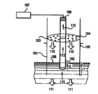
Fgure 1 provides an illustration of a scalable non-contact optical backscatter
insertion probe
according to the present invention.
Figures 2, 3A, 3B, and 4 provide examples of the results of analyses of the
data obtained by
a probe according to the present invention as used to measure water having
varying constituent
concentrations.
DETAILED DESCRIpTTON
The present invention will now be descn'bed with reference to the accompanying
drawings.
Figure 1 provides as illustration of a scalable non-contact optical
backscatter insertion probe
according to the present invention. As shown in Figure 1, the probe comprises
an outer optical
chamber 101, an inner optical chamber 102, a scalable and movable Iight table
103 having a number
of EME sources 104 positioned thereon, an optional mounting collar or bracket
105, a sensor 106,
and a processor 107.
The outer optical chamber 101 may have a cylindrical shape as shown in Figure
1 or other
shapes as are suitable for the applications for which the probe is utilized.
The outer optical chamber
may be made of a metal such as ahunituun, pvc-type plastic, a hardened fiber-
resin, Tetlon* type plastic,
or other suitable materials. The outside wall of the chamber may be coated
with an antifouling paint
or other anti-corrosive material, or metal substrate. The inner wall of the
chamber is coated with a
high renecrive coating.
* trade-mark
4
CA 02269620 2002-12-11
The inner optics;ll chamber 102 may have cylindrical shape as shown in Figure
1 or other shapes
as are suitable for the applications for which the probe iswsed. The inner
optical chamber 102 may
be made of a metal, plastic, fiber resin, or other suitable materials. The
outer surface of the Timer
optical chamber is highly reflective to insure that photons (EME) emitted by
the light source 104 do
not enter the inner optical chamber directly, but instead enter the inner
optical chamber only when
backscattered from the medium to be analyzed. The inner surface of the inner
optical chamber is
coated for highly absorbing ~ for most applications and may also be buffed to
prevent side-scatter
of photons off the walls of the inner chamber to insure that only direct
backscattered photons (EME)
reach the sensor 106. Alternatively, the inner surface of the ianer optical
chamber 102 may be a
highly reBectNe s~nface, e.g., a diffuse reflector, to eliminate any
polarization effects oflhe upwelled
light which may adversely affect the sensor's measurement of backscattered
EME. The coatings can
be any special paint or coating made of an emulsified powder, such as barium
sulfate or other dark
substrate such as carbon black or a mixture coating with carbon black. The
coating, whether high
or low reflective, should have a nearly diffuse lambertion reflectance.
The diameter of the inner optical chamber 102 is usually determined by the
field of view
(FOV) of the sensor 106. Generally, for liquid measurement applications, the
diameter of the inner
chamber is equal to or on the same order of size as the FOV. The length of the
outer optical chamber
101 is generally equal to or greater than the length of the inner optical
chamber 102. For example,
if the modium to be analyzed is a liquid, the inner optical chamber 102 is
positioned below the suzface
of the liquid to eliminate s<irFace reBectaace such that only subsurface
backscattered light is collected
by the sensor. The outer optical chamber 101 is also inserted into the medium
and extends beyond
the depth of the inner optical chamber 102 as illustrated in Figure 1. The
ends of the chambers 101
CA 02269620 1999-04-22
WO 98/20321 PCT/US97/20922
or 102 may be socluded from the environment or medium by a clear plastic or
lens type of fitting. In
Figure 1, X represents the depth of the inner optical chamber 102 below the
surface of the medium
108 and Y represents the depth of the outer optical chamber 101 below the
surface of the medium
such that X_<Y.
The preferred relative positioning of the inner and outer optical chambers
when the medium
is a solid or gas is generally equal to one another. However, if X<Y for a
solid, the surface
reflectance or surface baclcscattering is included in the measured
backscattered light by the probe.
Thus, the lengths of the inner and outer chambers and the effective diameter
of the inner and outer
chambers are scalable in dimensions. However, the inner chambei diameter must
be less than the
outer chamber diameter.
The light table 103 is also scalable to fit the dimensions of the outer
optical chamber 101 and
the inner chamber 102. The light table 103 is also movable along and within
the outer optical
chamber 101 to adjust the distance between the EME sources 104 and the medium
to be analyzed
as desired. The light table 103 has one or more EME sources 104 positioned
thereon. The EME
sources) 104 may be, for example, laser(s), LFD(s) or broad band light (e.g.,
halogen quartz or
tungsten) sources.
The sensor 106 may be a commerccdaally available monochrometer, spectrograph,
multi-
wavelength linear diode array (LDA), charge coupled device (CCD) or charge
induced device (Cm)
type sensor, any mufti-wavelength spectral sensor, silicon diodes or similar
light sensitive sensor.
According to a preferred embodiment of the present invention, the sensor 106
is a mufti-wavelength
linear diode array sensor with high radiometric, spectral and temporal
resolution mounted as a solid
state camera head. For example, in a study of multiple wavelength excitation
and emission
6
CA 02269620 1999-04-22
WO 98/20321 PCT/US97/20922
spo~roscopy, the sensor 106 may be an analog or digital camera, photo-
multiplier tube (P.M.T.) or
similar device, and the F.ME source 104 may be a laser; thus resolving
fluorescence backscatter
emission of the medium.
Data collected by the sensor 106 is provided to a remote processor via a
hardwired or wireless
data or signal link as are well-known in the art. The processor 107 receives
data collected by the
sensor 106 and processes the received data according to the particular
analysis to be performed. For
example, the data from the sensor may be analyzed by the processor 107 using
optimal passive or
active correlation spectroscopy techniques. The processor may also include one
or more storage
devices (not shown) for storing the received sensor data and the results of
the data analysis.
A processor for use in the present inv~tion may be, for example, an analog to
digital
converter integrated with a commercially available original equipment
manufacturer (OElI~
computer.
Notably, the scalable, non-contact optical backscatter insertion probe
according to the
pramt invention may also be used to measure reflectance and other optical
characteristics of the
medium as desired.
The operation of the nan~ntact optical ba~sc~ pmbe shown in Figure 1 is as
follows.
EME l I0 is emitted by EME sources 104 on light table 103. The emitted EME
enters the
medium to be analyzed as represaitod by arrows 111. Some of the EME 111 in the
medium is
backscat~ed by the medium or constituents in the medium. A portion 112 of the
backscattered
EME is colle<~d by the i~er optical chamber 102 and direcbad to the sensor
106. The sensor 106
generates signals in response to the received EME 112 and provides these
signals to processor 107
for processing.
7
CA 02269620 1999-04-22
WO 98/20321 PCT/US97I20922
The determination of chemical concentrations of constituents in a liquid
medium using a
non-contact optical backscatter insertion probe according to the present
invention may be
accomplished through the use of a multiple wavelength inversion methodology
which is derived
from radiative transfer theory, i.e., basic differential equations which
describe the two-flow nature
of ~ within a liquid medium and the water-air interface. This analysis may
combine a first,
second or higher order deaivative or inflection analysis of the optical
signatures for optimal band
detection followed by inversion techniques using solutions to differential
equations which conduct
an energy balance on the medium within a specified portion of the EM spectrum
(e:g., a specified
channel or waveband). The analysis technique may utilize solely derivative
spectroscopy.
Components of complex mixtures may also be determined through application of
eigenvalue
analysis of the optical signature of backscattered light. When a high degree
of precision is
required with chemicals with simitar optical bac~tter characteristics, optical
clean up techniques
can be used for signature analysis.
F~camples of measured relationships between the measured backscattered F.ME
spectrum
and the chemical composition of a liquid medium are illustrated in Figures 2
through 4. These
figums demonstrate the applicability of the probe to provide data sufficient
to determine chemical
or constituent conc~trations in water ranging from clear water to highly
turbid waters such as
typical wastewater or industrial process streams or water.
Figure 2 illustrates the variations in backscattered FrIyJE collected from
different types of
marine waters - from highly turbid fresh water (201) to cleaner, near-coastal
waters (202). Fsy
calculating both the magnitude and wavelength shifts of the backscattered EME
directly or
8
CA 02269620 1999-04-22
WO 98/20321 PCT/US97/20922
normalized to the ~ emitted into the water, the identity and concentration of
substances in the
water may be determined. Tl~ broader curves represent waters with more turbid
characteristics.
Figures 3A and 3B illustrate the relationship between the concentration of
total. suspended
matter (seston) in a complex water sample from an estuarine environment and a
measure of the
optical inflection (non-linear derivative estimator). Thus, the signatures of
light intensity of
subsurface backscattered light measured from the probe normalized to the EME
impinging from
the light table can be analyzed to predict the constituents in water as well
as selection of the
optimal wavelengths to use for detection or monitoring a medium.
Figure 4 ~h~sr<ates the relationship betw~n the concentration of chlorophyll
and a measure
of the optical inflection (at a diffaait location in the spoctrum than shown
in Figures 3A and 3B).
This graph illustrates the technique of measuring subsurface backscattered
light that can be used
to measure pigments in a liquid medium using the sensor, processor, scalable
probe, and analysis
procedures described above.
The non-contact scalable optical backscatter insertion probe according to the
present
invention is suited to numerous commercial applications, such as measurement
of concentration
of various materials in water, such as wastewater, and process slurries. Given
a specified waste
or process stream, the probe according to the print invention may be custom
designed (scaled)
for the application. The probe may also be integrated into a processing
plant's computer system
to provide information on the contents of wastewater, process slurries and
other media on a
continual basis and to create a continuous record of the concentration of
substances in the media.
Aaording to other embodiments of the present invention, the scalable probe may
also be
made much smaller, e.g., on the order of size as a fiber optic cable
(nominally S U.lcm) or the
9
CA 02269620 1999-04-22
WO 98/20321 _ PCT1LTS97/20922
size of a test tube or similar optical call. For example, living plant or
animal tissue types can be
assessed for composition and or texturally measured differences with the
backscattered light
dependent upon cellular level changes. The probe can also be used to measure
liquid substrates
or a gas placed in or flowing through a test tube or sample cell, with the
probe being inserted into
the top of the tube or cell. For example, the probe according to the present
invention may be used
for the analysis of bloods, pharmaceuticals, serums, chemical concentrates,
gases, etc.
While the present invention has boen particularly described with reference to
the preferred
embodiments, it should be readily apparent to those of ordinary skill in the
art that changes and
modifications in form and details may be made without departing from the
spirit and scope of the
invaition. It is intended that the appended claims include such changes and
modifications.