Note: Descriptions are shown in the official language in which they were submitted.
CA 02269688 1999-04-21
WO 98/18012 PCT/US97117966
METHODS AND APPARATUS FOR OSCILLATOR
COMPENSATION IN AN ELECTRICAL ENERGY METER
Field of Invention:
The present invention relates generally to the field of
utility company meters for metering electrical energy. More
particularly, the present invention relates to methods and
apparatus for maximizing the accuracy of oscillators used in
electronic watthour meters or other time sensitive devices.
Background of the Invention:
Meters for metering the various forms of electrical
energy are well known. Utility company meters can be of three
general types, namely, electro-mechanical based meters (output
generated by a rotating disk), purely electronic component based
meters (output component generated without any rotating parts) and
a hybrid mechanical/electronic meter. In the hybrid meter, a so-
called electronic register is coupled, usually optically, to a
rotating disk. Pulses generated by the rotating disk, for example
by light reflected from a spot painted on the disk, are utilized
to generate an electronic output signal.
It will be appreciated that the use of electronic
components in electric energy meters has gained considerable
acceptance due to their reliability and extended ambient
temperature ranges of operation. Moreover, contemporary
electronic signal processing devices, such as micro controllers,
have a greater accuracy potential for calculating electrical
energy use than prior mechanical devices. Consequently, various
CA 02269688 2002-09-13
WO 98/18012 PCT/US97I17966
_ 2 _
forms of electronic based meters have been proposed which are
virtually free of any moving parts.
Examples of electronic meters are disclosed in U.S.
Patent Nos. 5,548,527 - Hemminger et al. and 5,555,508 - Munday
et al. In those meters, signal
processing has been generally distributed between a digital signal
processing integrated circuit device and a micracontroller device.
As will be apparent, clock signal generation is necessary for the
operation of such devices. Indeed, for applications in which such
electronic devices are used to monitor time-based parameters, such
as time-of-use metering, the accuracy of such clock signals can
have a significant impact an the accuracy of the monitoring data.
In metering applications, clock signals are typically generated
in two ways, namely, in relation to the line frequency ox through
the use of an internal oscillator.
In the United States, quality clock signals can be
generated in relation to line frequency, i.e., the frequency of
the voltage signal being supplied to a given customer, which is
60 Hz. It is widely known that the frequency of the U.S. power
grid is extremely stable over long periods of time.
Internationally, the reliability of line frequency based clock
signals is inconsistent, particularly in third world countries.
In such environments, some other method is required for monitoring
time, such as internal oscillators.
In view of the above, an electronic based energy meter
will have maximum salability if it can monitor time accurately in
all environments, i.e., environments in which grid frequency is
stable and environments in which grid frequency is unstable.
Moreover, in time-of-use meters, the measurement of real time must
be maintained at all times, even during power outages. To these
ends, the meters described in the above patents incorporate two
crystal oscillators, one of the oscillators being used to measure
real-time during power outages, i.e., low power battery operation.
The accuracy of a crystal oscillator is its ability to
generate a consistent signal aver time. This characteristic is
described in terms of PPM (parts per million). A 1 MHZ crystal
which has an error of ~10 PPM will generate between 999,990 and
CA 02269688 1999-04-21
WO 98/18012 PCT/US97/17966
- 3 -
1,000,010 pulses every second. Since in metering applications,
customer billing is based on measured time, accuracy is very
important. Presently, many utility companies desire accuracies
of 5 PPM.
One method for ensuring accurate crystal oscillator
signals is to purchase commercially available oscillators having
the desired accuracy characteristics. Unfortunately, such
oscillators are relatively expensive and for high volume products
such as energy meters, such expense becomes economically
prohibitive. Moreover, during power outages, meters such as those
described in the above patents, go into a low power mode. 32.768
kHz crystal oscillators have been used for such low power
operations because they are inexpensive and well suited for low
power operation. Unfortunately, the initial and long term
accuracy of such crystals is commonly 50 PPM or greater.
Obtaining such an oscillator with the desired accuracy
specifications is also cost prohibitive.
Consequently, a need still exists for an electronic
meter which incorporates accurate, low cost, crystal oscillators.
Summary of the Invention:
The above problems are overcome and the advantages of
the invention are achieved in methods and apparatus for metering
electrical energy in an electronic meter. Such meter includes a
first oscillator for generating a first clock signal to within a
first accuracy and a second oscillator for generating a second
clock signal within a second accuracy. A processor, operable in
relation to a clock signal, measures time and periodically
compensates for the accuracy of the first oscillator. The first
clock signal is used for measuring time when power is applied to
the meter and the second clock signal is used by the processor for
measuring time when power has been removed from the meter. The
accuracy of the first oscillator is compensated periodically in
relation to a compensation factor stored in memory. In one
embodiment, the processor includes a counter for counting from a
first value to a second value in response to the first clock
signal. In such an arrangement, the processor substitutes the
CA 02269688 1999-04-21
WO 98/18012 PCT/LTS97/17966
- 4 -
first compensation factor for the first value. The meter can
further include a timer, wherein the processor substitutes the
first compensation factor for the first value in response to the
first timer. The processor also is shown to implement a process
for compensating for the accuracy of the second oscillator. This
process compensates for the accuracy of the second oscillator in
relation to the first oscillator. To this end, the process
calculates a second compensation factor. The second compensation
factor is determined when power is applied to the meter, wherein
after power has been removed and restored, the second compensation
factor is used to compensate time measured in relation to the
second oscillator during the period power had been removed.
Brief Description of the Drawings:
The present invention will be better understood, and its
numerous objects and advantages will become apparent to those
skilled in the art by reference to the following detailed
description of the invention when taken in conjunction with the
following drawings, in which:
Fig. 1 is a block diagram of an electronic meter
constructed in accordance with the present invention;
Fig. 2 is a block diagram of the A/D & DSP processor
shown in Fig. 1;
Fig. 3 is a flow chart of programming implemented in the
microcontroller disclosed in Fig. 1;
Fig. 4 is a block diagram of timers, software counters
and programming implemented in the microcontroller disclosed in
Fig. 1; and
Fig. S is a more detailed flow chart of a portion of the
programming disclosed in Fig. 3.
Detailed Description:
A new and novel meter for metering electrical energy is
shown in Fig. 1 and generally designated 10. It is noted at the
outset that this meter is constructed so that the future
implementation of higher level metering functions can be
supported.
CA 02269688 2002-09-13
WO 98118012 PCTlL1S9711'l9bb
S -
Meter 10 is shown to include three resistive voltage
divider networks 12A, 128, 12C; a first processor 14 - an ADC/DSP
(analog-to-digital converter/digital signal processor) chip
(hereafter DSP 14); a seco~ processor 16 - which in the preferred
S embodiment is a Mitsubishi Model M38207 microcontroller (hereafter
MCU 16); three current sensors 18A, 18B, 18C; a 12V switching
power supgly 20 that is capable of receiving inputs in the range
of 96-528V; a 5V linear power supply 22; a non-volatile power
supply 24 that switches to a battery 26 when 5V supply 22 is
inoperative; a 2.5V precision voltage reference 28; a liquid
crystal display (LCD) 30; a 32.768 kHz crystal oscillator 32; a
12.28608 MHZ crystal oscillator 34 that provides a timing signal
to chip 14, which timing signal is divided by 2.0 to provide a
6.14304 MHZ clock signal to MCU 16; 16 kByte of EEPROM 35; a
serial communications line 36; an option connector 38; and an
optical communications port 40 that may be used to read the meter.
The 6.14304 MHZ clock signal can be used as the system
clock. It is noted that a signal representative of line frequency
is also provided, shown as 120 Hz in Fig. 1. In the preferred
embodiment, this line frequency is representative of the line
frequency of the phase A voltage. Except for certain aspects of
DSP 14, MCU 16, LCD 30, crystal oscillator 32, crystal oscillator
34 and EEPROM 35, the interrelationship of all components shown
in Fig. 1 is set forth in U.S. Patent No. 5,555,508
During power outages, MCU 16 switches to a low power
mode of operation, in which oscillator 34 or the line frequency
ceases to be the source of the system clock and oscillator 32
becomes the alternate system clock. In that mode, oscillator 32
is used as the time base for determining power outage duration.
In the preferred embodiment, oscillator 34 is selected
to be relatively stable, i.e., within 3 parts per million (PPM)
long term. However, its actual frequency may be offset slightly
from the nominal value. Oscillator 32 is selected to be less
stable over time, i.E., about 50 PPM. While such an operating
characteristic is poor for long term operations, it is well known
that crystal oscillators of this type: do exhibit good short term
w
CA 02269688 1999-04-21
WO 98/18012 PCT/LJS97/17966
- 6 -
stability. One aspect of the invention takes advantage of this
short term stability and compensates for long term instability
resulting in an acceptable low cost crystal oscillator.
In the preferred embodiment of meter 10, two levels of
oscillator compensation are utilized to account for long term
stability. First, oscillator 34 is corrected for any deviation
from its manufacturer listed value by using MCU 16 to apply a
constant offset correction factor. Thus a stable time base is
provided while power is ON. The offset factor for oscillator 34
can be determined during assembly by operating the oscillator,
measuring its output for a period of time and comparing such
output to its nominal value for that same period of time. The
resulting offset value can be stored in memory 35 for later use,
as will be described, by MCU 16.
Second, the corrected output of oscillator 34 is used
by MCU 16 to monitor the output of oscillator 32 in real-time.
Such real-time monitoring is accomplished by causing MCU 16 to
calculate a correction factor, based in part on the corrected
output of oscillator 34, for oscillator 32. During power outage,
using battery 26, MCU 16 keeps track of time based on oscillator
32. When power is restored, MCU 16 corrects the outage time by
multiplying the measured time by the last determined correction
factor. This outage time is stored and is added to the time the
power outage began in order to determine the current time.
Before describing in detail the compensation process,
consider first the overall operation of meter 10.
METER OPERATION
It will be appreciated that electrical energy has both
voltage and current characteristics. In relation to meter 10,
voltage signals are provided to resistive dividers 12A-12C and
current signals are induced in a current transformer (CT) and
shunted. The output of CT/shunt combinations 18A-18C is used to
determine electrical energy.
First, DSP 14 is connected to receive the voltage and
current signals provided by dividers 12A-12C and shunts 18A-18C.
As will be explained in greater detail below, DSP 14 converts the
voltage and current signals to voltage and current digital
CA 02269688 1999-04-21
WO 98/18012 PCT/US97/17966
_ 7 _
signals, determines electrical energy from the voltage and current
digital signals and generates an energy signal representative of
the electrical energy determination. DSP 14 will always generate
watthour delivered (Whr Del) and watthour received (Whr Rec)
signals, and depending on the type of energy being metered, will
generate either volt amp reactive hour delivered (VARhr Del)/volt
amp reactive hour received (VARhr Rec) signals or volt amp hour
delivered (VAhr Del)/volt amp hour received (VAhr Rec) signals.
In the preferred embodiment, each transition on conductors 42-48
(each transition from logic low to logic high or vice versa) is
representative of the measurement of a unit of energy. MCU 16
receives the energy signals) and generates an indication signal
representative of the energy signal.
In relation to the preferred embodiment of meter 10,
currents and voltages are sensed using conventional current
transformers (CT's) and resistive voltage dividers, respectively.
The appropriate multiplication is accomplished in a new integrated
circuit, i.e. DSP 14. Although described in greater detail in
relation to Fig. 2, DSP 14 is essentially a programmable digital
signal processor (DSP) with built in analog to digital (A/D)
converters. The converters are capable of sampling three input
channels simultaneously at up to 14,400 Hz each with a resolution
of 20 bits and then the integral DSP performs various calculations
on the results.
Meter to can be programmed to operate as a time of use
(TOU) meter. It will be recognized that TOU meters are becoming
increasingly popular due to the greater differentiation by which
electrical energy is billed. For example, electrical energy
metered during peak hours can be billed differently than
electrical energy billed during non-peak hours. As will be
explained in greater detail below, DSP 14 determines units of
electrical energy while MCU 16, in the TOU mode, qualifies such
energy units in relation to the time such units were determined,
i.e. the season as well as the time of day.
Most indicators and test features are brought out
through the face of meter 10 (not shown) , either on LCD 30, by
elastomer switch inputs, or through optical communications port
CA 02269688 1999-04-21
WO 98/18012 PCT/CTS97/17966
_ g _
40. In addition, other connections such as relay outputs or
remote communications can be brought out through the base of the
meter via option connector 38. Power supply 20 for the
electronics is a switching power supply feeding low voltage linear
supply 22. Such an approach allows a wide operating voltage range
for meter 10.
In the preferred embodiment of the present invention,
the so-called standard meter components and register electronics
are all located on a single printed circuit board (not shown)
defined as an electronics assembly. This electronics assembly
houses power supplies 20, 22, 24 and 28, resistive dividers I2A-
12C for all three phases, the shunt resistor portion of 18A-18C,
oscillator 34, DSP 14, MCU I6, EEPROM 35, oscillator 32, optical
port components 40, LCD 30, and an option board interface 38.
Configuration and billing data is stored in EEPROM 35. This same
assembly is used for TOU metering applications by merely utilizing
battery 26 and reprogramming the configuration data in EEPROM 35.
It will be appreciated that energy units are calculated
by DSP 14 primarily from multiplication of voltage and current.
The specific formulae utilized in the preferred embodiment are
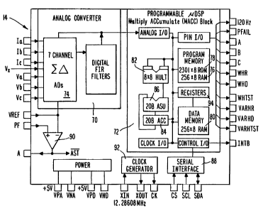
listed in Table 1. As shown in Fig. 2, DSP 14 includes A/D
converters 70 and a programmable DSP 72.
In the preferred embodiment, the three voltage inputs,
Va, Vb and Vc are sampled by one of the A/D's and the three
current inputs Ia, Ib and Ic are sampled by a second A/D. The
third A/D is used to sample either Va, Vb, Vx or Ib. Such
sampling of the voltage or current input at the third converter
is done because for certain applications an additional signal is
desired to be sampled at the same time as the voltages and
currents of the other phases. As an example, so-called two
element meters require the B phase voltage to be combined with the
other phase voltages to produce the line-to-line voltage. Having
a third A/D enables these terms to be sampled simultaneously,
thereby improving the measurement accuracy. This also improves
the signal to noise ratio within DSP 14.
The additional input Vx is provided as a spare channel
input. One application is to use this channel to do temperature
CA 02269688 1999-04-21
WO 98/18012 PCT/US97/17966
_ g _
compensation by providing an input signal that is representative
of temperature to the Vx input and then using the DSP to further
compensate the reference voltage.
DSP 72 is a reduced instruction set (RISC) processor
which computes the desired energy quantities from the converted
voltage and current samples. DSP 72 is shown to incorporate a
random access memory (RAM) memory 80 having a capacity of 256
bytes of data. Memory 80 is used to store computations and the
subroutine stack. A read only memory (ROM) 78 is also shown and
has a capacity of 2,304 bytes of data. Memory 78 is used to store
those metering subroutines common to general energy calculations.
Another RAM memory 76 is depicted and has a capacity of 256 bytes
of data. Memory 76 is used to store the main-line program and
specialized subroutines of DSP 72.
DSP 72 is also shown to include multiplier 82 and an
accumulator 84 for processing the voltage and current digital
signals thereby generating electrical energy information. Also
included is an arithmetic subtraction unit 86 interposed between
multiplier 82 and accumulator 84.
From the foregoing, it should be appreciated that
program ROM, i.e. memory 78 is defined at the oxide via level.
As this defining step occurs relatively late in the manufacturing
process for DSP 14, changes can be made to such programming with
minimal effort.
Calibration constants for each phase and certain
potential linearization constants are stored in memory 80.
Memories 76 and 80 are serially down loaded from EEPROM 35 by MCU
16 on power-up of meter 10. Such an embodiment allows the
benefits of being able to provide various meter forms economically
and to calibrate without hardware modification. It also permits
the future addition of metering VAR or VA. The formulae for such
operations are included in Table 1. Furthermore, the calculation
of future, yet undefined, complex metering quantities could be
obtained by merely reprogramming DSP 14.
DSP 14 also contains a serial interface 88, power fail
detect circuitry 90, and potential present outputs A, B and C.
DSP 14 is provided a clock signal by a 12.28608 MHZ crystal
CA 02269688 1999-04-21
WO 98/18012 PCT/ITS97/17966
- 10 -
oscillator 34. DSP 14 uses this signal directly for driving the
DSP and indirectly for the A/D sampling. This frequency is also
operated upon by clock generator 92 which serves to divide the
output of oscillator 34 (input to DSP 14 at XIN and XOUT) by 2.0,
to buffer the divided clock signal and to output the 6.14304 MHZ
clock signal at CK to MCU 16. This clock output is specified to
work down to a supply voltage of 2.0 VDC.
Power fail detection circuit 90 is a comparator which
compares a divided representation of the 12 V power supply voltage
20 to a precision reference. A power fail signal (PFAIL) is
provided upon loss o'f the power supply voltage 20. Upon power
fail, it is preferable to reset DSP 14. In such a situation, the
output pins Whr, Whd, etc. are forced to logic low voltage levels.
Additionally, DSP 14 goes into a lower power mode to reduce the
current draw on power supply 22. In this lower power mode the
comparator and oscillator operation are not affected, but DSP 72
ceases to operate.
The phase A, B and C potential indicator outputs are
under control of DSP 14 and are generally indicative of the
presence of voltage. Although not shown, it is noted that the A,
B and C outputs are logic level outputs generated in response to
comparing the voltage of each phase to a programmable threshold.
A signal line, labeled 120 Hz in Figs. 1 and 2, provides a
frequency proportional to the received line frequency, namely,
a frequency of two times the line frequency. This frequency can
be used by MCU 16 in an alternate configuration to keep time based
on line frequency.
CA 02269688 1999-04-21
WO 98/18012 PCT/US97/17966
- 11 -
OSCILLATOR OPERATION
Consider now the operation of crystal oscillators 32 and
34 and their interaction with MCU 16. It is assumed for purposes
of explanation that line frequency, commonly 50 or 60 Hz, is not
being used to measure time, but rather, oscillators 34 and 32 are
being used for this purpose. However, it will be appreciated
after reviewing the below explanation that whether the system
(grid) frequency or internal oscillator 34 is being used to
measure time, the oscillator compensation operations will be
carried out.
During power ON operation, MCU 16 receives its 6.14304
MHZ clock input from DSP 14 as described above. This signal is
divided by sixteen (16) and the resultant signal (383,940 Hz) is
used to drive a first timer, TIMER X (designated as 132 in Fig.
4). This first timer is used to keep time during power ON
operation. Upon the occurrence of a power fail, MCU 16 shifts to
the 32.768 kHz crystal oscillator 32 for tracking time in a low
power mode. To this end, a WIT instruction is executed which
places MCU 16 in a mode where only the 32.768 kHz oscillator and
associated timers are operational. While in this mode a timer is
set to "wake up" MCU 16 every 32,768 cycles of oscillator 32 to
count a second.
It will be appreciated from the following description
that the control of various timers, the capture of various timer
values and the calculation of oscillator compensation are
preferrably achieved in software implemented in MCU 16. The
invention is not limited to that particular implementation.
However, for purposes of explanation it will be so described.
Consider first the flow chart shown in Fig. 3.
In order to compensate for oscillator instability, MCU
16 first initializes certain functions at 100. The need for
initialization occurs when MCU 16 goes into reset, which is the
case when the voltage from non-volatile supply 24 falls below
approximately 2.5 volts. Otherwise, MCU 16 performs operations
to restore from a power outage, which occurs at 102.
During initialization, MCU 16 will initialize or set
certain parameters so that oscillator compensation can begin.
CA 02269688 1999-04-21
WO 98/18012 PCT/US97/17966
- 12 -
Oscillator 32 is corrected by dynamically calculating a correction
factor (hereafter CF32) during power ON operation and then
modifying the outage duration time measurement made in relation
to oscillator 32 during power OFF operation by CF32. To this end,
CF32 will be some numerical value between zero and 2Ø During
initialization CF32 is set to 1.0, its nominal value when
oscillator 32 is exactly correct.
As will be explained in greater detail in relation to
Figs. 4 and 5, CF32 is calculated in relation to the measurements
made by various timers, namely TIMER X (designated 132 in Fig. 4)
and TIMER Y (designated 150 in Fig. 4) and seconds counter
NUMSEC32 (designated 154 in Fig. 4). In the preferred embodiment,
TIMER X and TIMER Y are MCU hardware timers, each of which are set
with a value from which they count down to zero in response to a
clock signal. During initialization, TIMER X and TIMER Y are
provided with default values. In the preferred embodiment, TIMER
X is set to 2,999 and TIMER Y is set to 32,768. The significance
of these values is described below in relation to Fig. 4.
NUMSEC32 is a software timer.
Normally, MCU 16 will be operating in a main loop
routine where power is ON and meter 10 is measuring and recording
electrical energy consumption or generation. However,
occasionally power will be removed, for example during a power
outage. When power is restored, MCU 16 only performs the
initialization routine if it lost battery carryover and went into
reset, as described above. Otherwise, MCU 16 performs operations
to restore from the power outage, which occurs at 102.
It will be recalled from above, that MCU 16 compensates
for the stability limitations of oscillator 32 by calculating
CF32. This calculation is achieved using the values X0, X1, Y1
and SAVSEC32, where XO is the count of TIMER X at the beginning
of the current interval, X1 is the count of TIMER X at the end of
the current interval, Y1 is the count of TIMER Y for the current
interval and SAVSEC32 is the count of the number of seconds at the
end of the current interval counted in NUMSEC32 in response to the
operation of oscillator 32. All of these operations are explained
in greater detail in relation to Fig. 4. In addition, MCU 16
CA 02269688 1999-04-21
WO 98/18012 PCT/US97/17966
- 13 -
compensates oscillator 34 and calculates CF32 after the conclusion
of certain time intervals. These intervals are determined by
timers called for discussion purposes COMP12 and COMP32
(designated 142 and 144, respectively, in Fig. 4l. These timers
count up from zero to some interval value. During restore,
COMP12 and COMP32 are initialized.
As will be described in relation to Fig. 4, it will be
seen that the COMP12 timer is set to 10 seconds and COMP32 timer
is set to 20 seconds. However, it is desirable for COMP32 and
COMP12 timers to not finish their respective intervals at the same
time, which can happen since the desired values are multiples of
each other. Consequently, during restore 102, the interval values
are initially set so the COMP32 interval starts first, the COMP12
interval starts 5 seconds later. 10 seconds later the COMP12
interval ends and oscillator 34 is compensated. 5 seconds after
that COMP32 interval ends and CF32 is calculated.
After restore 102, MCU 16 enters into a main loop
program, three steps of which are shown in Figure 3. It will be
appreciated that the main loop program contains many items other
than what is shown in Fig. 3, however, the steps shown in Fig. 3
are necessary to achieve the desired oscillator compensation. The
three steps include, reacting to a power fail interrupt, at 104,
reacting to an executive clock interrupt, at 106, and calculating
a new CF32, determined at 108.
The determination of a power fail interrupt at 104 is
indicative that a power failure has been detected and that power
is about to be lost. Such an interrupt will be generated in
response to the detection of an appropriate signal on the PFAIL
output from DSP 14. In such a situation MCU 16 will begin at 110
to process the power fail interrupt and begin the low power mode.
It will be recalled that, during low power mode, MCU 16 will
"sleep" and "wake-up" in relation to oscillator 32. As shown in
Fig. 4, MCU 16 via TIMER Y, counts a second at 112 and determines
at 114 whether power has come back on. If power has not been
restored, MCU 16 returns to 112 to count another second when TIMER
Y reaches the appropriate count. When power is restored, MCU 16
starts full power operation at 116. The number of seconds counted
CA 02269688 1999-04-21
WO 98/18012 PCT/US971I7966
- 14 -
during the power outage is modified, i.e., multiplied, at 118 by
the last calculated CF32 before power was lost. This compensated
value, in addition to being recorded as the outage duration, is
added to the last known date and time at 120 in order to establish
also the current date and time. MCU 16 then returns to the
restore operations at 102.
If no power fail interrupt is pending at 104, MCU 16
next determines the presence of an executive clock interrupt
request at 106. If such a request is present, MCU 16 processes
the interrupt at 122; executive clock interrupt operations include
determining whether it is time to compensate for oscillator 34,
monitoring oscillator 32 and counting power ON seconds. Although
these operations will now be generally described, they are more
particularly described in relation to Fig. 5. As will be
described in Fig. 4, the executive clock interrupt occurs whenever
TIMER X counts 1/128 of a second, i.e., every 7.8125 ms.
At 122, MCU 16 determines whether the correction factor
necessary to compensate oscillator 34 (hereafter CF12) was loaded
into TIMER X. TIMER X is preferably a countdown timer which over
a period of 10 seconds will count from a specified default reload
value (hereafter DEFAULT12, designated 134 in Fig. 4) generally
representative of a 1/128 second interval for a clock signal
originating from oscillator 34 and at this point having a
frequency of 383,940 Hz (preferably DEFAULT12 is 2,999) down to
zero 1,279 times. The 1280th operation of TIMER X will involve
the timer counting down to zero from the compensation value
determined during manufacture, i.e., CF12 (designated 136 in Fig.
4). In the preferred embodiment, CF12 is determined by measuring
the actual frequency of oscillator 34 and applying the following
formula:
CF12 - ((measured frequency - 6,143,040Hz)/l.6Hz)+2999+680
value rounded to nearest integer
If MCU 16 determines at 122 that TIMER X just counted
down from CF12 to zero, it reloads TIMER X with DEFAULT12, i.e.,
the 2999 value. In the preferred embodiment, if the memory area
CA 02269688 1999-04-21
WO 98/18012 PCT/US97/17966
- 15 -
where CF12 is stored appears corrupt, for whatever reason, MCU 16
will use a nominal compensation value (preferably 2999 + 680). If
it is determined that TIMER X just counted from CF12, MCU 16 also
resets the flag which signals that compensation of oscillator 34
was just performed.
At 122, MCU 16 also maintains the seconds count from
TIMER Y. It will be recalled that TIMER Y is driven by oscillator
32 which operates at 32.768 kHz and that TIMER Y counts down to
zero preferably from the value 32,768 (hereafter COUNT32,
designated 152 in Fig. 4). Consequently, every time TIMER Y
reaches zero, 1 second will have passed, if oscillator 32 is
stable. Preferably, TIMER Y is automatically loaded with COUNT32,
via a reload register, each time TIMER Y reaches zero and a flag
is set indicating that TIMER Y reached zero. Consequently, at 122
MCU 16 looks to see if the TIMER Y reload flag is set. If it is,
MCU 16 counts 1 second in NUMSEC32 (count of oscillator 32 based
seconds) and resets the reload flag.
At 122, it is also desirable to count each second
determined by TIMER X. It will be recalled that TIMER X is
counting down to zero in roughly 1/128th of a second increments.
Accordingly, a counter (hereafter SECCNTR, designated 138 in Fig.
4) is provided which counts down from 128 each time TIMER X
reaches zero. When SECCNTR reaches zero, it provides a signal
indicative of the passage of 1 second of time (used for power ON
timekeeping). The executive clock interrupt (designated 140 in
Fig. 4) is driven by this counter. When it is determined that a
second has passed, a number of boundary routines are performed.
First a check is made to determine if the time has been
reached to correct oscillator 34. To this end, COMP12 counts up
from zero to 10 seconds at each second indication from SECCNTR.
When COMP12 reaches 10 seconds, MCU 16 causes CF12 to be loaded
into TIMER X. COMP12 will then begin again to count up from zero
to 10 seconds.
Another boundary routine is to determine whether the
time has come to compensate oscillator 32, i.e., calculate a new
CF32. Similar to determining if the COMP12 time period has
passed, MCU 16 uses COMP32 timer which counts up from zero to 20
CA 02269688 1999-04-21
WO 98/18012 PCT/US97/17966
- 16 -
seconds each time an indication is given by SECCNTR that a second
has passed. Once MCU 16 determines that 20 seconds have passed,
it calculates a new CF32 at 124. COMP32 then begins again to
count up from zero to 20 seconds.
Before describing the process performed at 122 and 124,
to calculate a new CF32, consider the flow of data as shown in
Fig. 4. In Fig. 4, the 6.14304 MHZ clock signal is received from
DSP 14 and divided by 16 by divider 130. The resulting 383,940
Hz clock signal is provided to TIMER X (132). TIMER X counts
down, 1,279 times during a 10 second interval, from a default
value DEFAULT12 (134) to zero loaded from reload register 133.
On the 1,280th time, register 133 is loaded with offset value CF12
(136) .
When timer 132 reaches zero, a clock signal is provided
to SECCNTR (138) which determines the passage of a second. To
make this determination, SECCNTR 138 is loaded with a count value,
preferably 128. SECCNTR 138 will count down to zero. When
SECCNTR 138 reaches zero, a clock signal is provided. This clock
signal is approximately 1 Hz and is indicative of the passage of
1 second of time. The clock signal from SECCNTR 138 is provided
to timers COMP12 (142) and COMP32 (144) . COMP12 counts up from
zero to 10 seconds. When COMP12 reaches 10 seconds, a flag is set
indicating that it is time to again compensate oscillator 34.
COMP32 (144) counts up from zero to 20 seconds. When COMP32
reaches 20 seconds, a flag is set indicating it is again time to
calculate a new compensation value CF32 for oscillator 32.
While TIMER X (132) is counting, the clock signal
generated by oscillator 32 is provided to TIMER Y (150). TIMER
Y is loaded, via load register 151, with a default value COUNT32
(152). TIMER Y (150) counts down from the loaded default value
to zero in response to the signal from oscillator 32. Each time
TIMER Y (150) reaches zero, it provides a clock signal (ideally
1 second) to counter NUMSEC32 (154). NUMSEC32 (154) counts the
number of times TIMER Y (150) reaches zero.
The operation of MCU 16 at 122 in Fig. 3 can also be
understood in relation to the flow chart shown in Fig. 5. Fig.
5 is a detailed flow chart of 122 in Fig. 3. At 160 a
CA 02269688 1999-04-21
WO 98/18012 PCT/US97/17966
- 17 -
determination is made as to whether a 12 MHz compensation has just
occurred. If such compensation has occurred, TIMER X reloads a
default value at 162. At 164 a determination is made of whether
TIMER Y just reloaded. If TIMER Y has just reloaded, NUMSEC32 is
incremented at 166. If TIMER Y has not just reloaded or once
NUMSEC32 has been incremented, SECCNTR is decremented at 168.
A determination is made at 170 if the count in SECCNTR
is zero. If it is not, a complete second has not yet passed.
Accordingly, it is not yet time to perform the boundary routines.
If the count in SECCNTR does equal zero, SECCNTR is reset to the
value 128 at 172. At 174 a signal is provided indicating that 1
second has passed. COMP12 is incremented at 176 and a
determination is made at 178 if the count in COMP12 equals 10.
If the count in COMP12 equals 10, COMP12 is reset to zero at 180.
TIMER X is then reloaded at I82 with the compensation factor CF12
and a signal is given at 184 that the 12 MHz compensation is in
progress. Once the 12 MHz compensation signal is given or if it
is determined at 178 that the count in COMP12 does not equal 10
seconds, the count in COMP32 is incremented at 186.
A determination is made at 188 whether COMP32 equals 20.
If COMP32 does not equal 20, then it is not yet time to calculate
CF32 and the routine ends. If it is determined that COMP32 does
equal 20, COMP32 is reset to zero at 190. At 200 the term XO is
made equal to the last determined X1 count. It will be recalled
that XO represents the count of TIMER X at the beginning of the
20 second interval, which is the same as the count at the end of
the previous interval. Accordingly, XO is made equal to the last
determined X1. The routine then waits at 202 for the next tick
of TIMER Y.
At 204, X1 is made equal to the current value of TIMER
X . This value will be the count of TIMER X at the end of the
current interval. At 206, Y1 is made equal to the count existing
in TIMER Y. A determination is made at 208 if TIMER Y just
reloaded. If TIMER Y just reloaded, the count in NUMSEC32 is
incremented. At 209 SAVSEC32 is set equal to the current value
of NUMSEC32 and at 211 NUMSEC32 is then set equal to zero. At
CA 02269688 1999-04-21
WO 98/18012 PCT/IJS97/17966
- 18 -
212, a signal is generated to run the 32 kHz correction factor
calculation and smoothing routine.
Consider now the 32 kHz oscillator compensation process
beginning at 190 in Fig. 5. In order to calculate a new CF32, MCU
16 must first gather certain information, i.e., take a "snapshot"
or get the values of certain timers and counters. To this end,
MCU 16 sets COMP32 equal to zero at 190. MCU 16 then sets the
term XO equal to the TIMER X term X1 (200 Fig. 5) from the prior
CF32 calculation. It is noted that the count in TIMER X is used
in the calculation of CF32 in order to account for the small
offset in time that will occur while MCU 16 is cycling through its
programming to reach the CF32 calculation routine.
At 202, MCU 16 next determines when TIMER Y has
generated its next "tick" or count transition (occurs
approximately every 30.5 ~,s). When MCU 16 makes this
determination, it reads the count then existing in TIMER X and
saves or stores this count in X1. MCU 16 then reads the count in
TIMER Y and saves this count in Y1. MCU 16 then determines if the
tick of TIMER Y that it just waited for was the tick that caused
TIMER Y to reload. This is achieved by checking to see if the
TIMER Y reload flag is set. If that is the case, then MCU 16
increments the count at NUMSEC32 (154). MCU 16 then saves the
count in NC1MSEC32 in SAVSEC32 and sets NUMSEC32 to zero. The four
variables needed to calculate CF32 are now saved in X0, X1, Y1 and
SAVSEC32. MCU 16 then sets a flag indicating that a new CF32 is
ready to be calculated. Waiting for the next tick of TIMER Y
minimizes an error which would otherwise be introduced to the
compensation process. Since the next tick of TIMER Y might be the
one which causes TIMER Y to reload, the TIMER Y reload flag is
checked. It is further noted that this must be a continuous
ongoing process in order to be able to use the prior calculation's
term X1 as the next calculation's term X0.
Consider now the process which occurs at 122 in Fig. 3.
MCU 16 then reads the count in seconds counter 154. Here, MCU 16
calculates the correction factor CF32 to compensate for the
inaccuracy in oscillator 32. Using the corrected l2MHz oscillator
as the ideal, MCU 16 counts the number of oscillator ticks within
CA 02269688 1999-04-21
WO 98/18012 PCTIUS97/17966
- 19 -
a 20 second interval. The ratio of this value to the ideal is the
correction factor. In the preferred embodiment, the correction
factor is run through a smoothing function which enables more long
term determinations. Such long term determinations tend to smooth
out any sudden changes in the correction factor.
In the preferred embodiment, the formula for calculating
the 32kHz correction factor is as follows:
CF32=32,768*[(XO-X1)+(20*383,940)]
[y+(32,768*SAVSEC32) ] *383, 940
Where:
CF32 - this iteration's correction factor
XO = TIMER X initial sample
X1 = TIMER X ending sample
Y - TIMER Y ending sample subtracted from 32768, i.e.,
32768 - Y1. The subtraction is needed since in the
preferred embodiment, TIMER Y is a down counter.
Since equation (1) can yield large values in both
numerator and denominator, the following equation is used to
preserve resolution:
CF32= 20*32,76B
( SAVSEC32 * 3 2 , 7 6 8 ) +y
+ x0-x1
[ (y/32, 768) +SAVSEC32] *383, 940
In the preferred embodiment the correction factor is
calculated by first determining y as y = 32768 - Y1 and then using
the following:
cF32=(655360/((sAVSEC32*32768)+y))
CA 02269688 1999-04-21
WO 98/18012 PCT/LTS97/17966
- 20 -
Using an exponential smoothing filter to apply the
+((x0-x1)/(((y/32,768)+SAVSEC32)*383940))
iteration's correction factor is preferred. One such smoothing
filter is as follows:
F1=CF32* (1/M) +FD* ( (M-1) /M)
where:
F1 = new filter correction factor
FO = old filter correction factor
CF32 = current iteration correction factor
M - filtering constant.
In the preferred embodiment, M is chosen to be 32. This
provides an appropriate time constant and enables the equation to
be easily implemented with additions and bit shifts.
CA 02269688 1999-04-21
WO 98/18012 PCT/US97/1796b
- 21 -
TABLE 1
Meter Formulae
Watt formulae
-3 : Wa t ts=K~ ( KAVA IA +KBVB IB +K~V~ I~ )
0 o i i Z z
-2 : Wa t t s =K~ ( ( KA VA -KBVB ) IA + ( K~V~ -KDVB ) I~ )
0 0 o z z z
-8 : Wa t ts=K~ ( KAVA IA - ( KBVA IB +KBV~ IB ) +K~V~ I~ )
0 o i i i i z z
-7 : Wa t t s =KG ( KAVAo IAo -KBVAo I Bo +KcVcz I cz )
NOTE: Subscripts refer to the phase of the inputs.
Sub-subscripts refer to the A/D cycle in which the
sample is taken. Va for -7 applications is actually
line to neutral.
VA Formulae
-3: VA=KG[ (KAVAo) rmslAorms+ (KBvBl) rmslElrms+ (KCVCZ) rmsICZrms~
-2: VA=KG( (KAVAo-KBVBo) rmslAorms+(Kcvcz KDVBz) rmslCZrms)
-8: VA=KG(KAVAormsIAorms KB( VAl+VCl) rmslBlrms+KCvCZrmsIc2rms~
CA 02269688 1999-04-21
WO 98/18012 PCT/US97/17966
- 22 -
-7 : VA=KG ( KAVAorms'T Aorms +KB VAorms IBorms+KCVCzrms ICZrms )
RMS measurements are made over one line cycle and
preferably begin at the zero crossing of each voltage.
VAR Formula
VAR= VAA2-WattAZ+ VABZ-WattB2+ VA~2-Watt~2
where the subscripts are associated with the I terms of
Watts and VAs and the calculation is performed every
cycle as shown below:
-3 : VAR=K ( K ( V I ) 2 _ ( ~''cyc~e VA IA ) z +
G A Aozms Aorms zero 0 0
K (V I ) 2- (rcycle V I ) 2+K ( V I ) Z- (cycle V I 2)
8 Blrms Blrms Lrzero Bl Bl CZrms CZrms zero CZ CZ )
-2 : VAR=K ( ( ( K V -K V ) I ) 2 _ (cycle ( K V -K V ) I ) 2 +
G A A~ B Bo zms Aorms zero A Ao B Bo Ao
cycle
( ( KCVC2 -KoVB2 ) rms I CZrms ) ( zero ( KCVCZ -KoVB2 ) I CZ ) )
-8: VAR=K (K (V r ) 2- ('cycle V I ) 2+
G A Aorms Aorms zero Ao Ao
CA 02269688 1999-04-21
WO 98/18012 PCT/US97117966
- 23 -
cycle
( - ( K&VA rms+KpVc rms ) 'IB rms ) ( zero ( KBVA jB +KoV~ j8 ) ) 2 +
2 o z o 0 o z x
K ( V j ) 2 _ ( cycle V j 2
Czrms CZrms zero Cz C2 ) )
Z _ cycle 2 2 _ cycle ) 2
-7 : VAR=K~ ( KA ( VAorms jAorms ) ( zero VAo jAo ) +KH ( VAOrms jeorms ) (
zero VA -rH +
0 0
K (V j )2_(~oYcIeVCIC)2)
CZrms CZrms zero Z Z
For purposes of the above formulae, the following
definitions apply:
-2 means a 2 element in 3 wire delta application;
-3 means a 3 element in 4 wire wye application;
-8 means a 2 ;~ element in 4 wire wye application;
-5 means a 2 element in 3 wire delta application;
-7 is a 2 ~ element in 4 wire delta application.
While the invention has been described and
illustrated with reference to specific embodiments, those
skilled in the art will recognize that modification and
variations may be made without departing from the principles
of the invention as described herein above and set forth in
the following claims.