Note: Descriptions are shown in the official language in which they were submitted.
CA 02269709 1999-04-23
- 1 -
DESCRIPTION
SINGLE CRYSTAL SIC AND PROCESS FOR PREPARING THE SAME
Technical Field
The present invention relates to single crystal SiC and
a method of producing the same, and more particularly to sin-
gle crystal SiC which is used as a semiconductor substrate
wafer for a light-emitting diode, an X-ray optical element
such as a monochrometer, a high-temperature semiconductor
electronic element, a power device, or the like, and also to
a method of producing the same.
Background Art
SiC (silicon carbide) is superior in heat resistance and
mechanical strength than an existing semiconductor material
such as Si (silicon) and GaAs (gallium arsenide), and also has
good high-temperature properties, high-frequency properties,
dielectric strength, and resistance to environments. In addi-
tion, it is easy to perform the valence control of electrons
and holes by doping an impurity. Moreover, SiC has a wide band
gap (for example, single crystal 6H-SiC has a band gap of
about 3.0 eV, and single crystal 4H-SiC has a band gap of 3.26
eV). For these reasons, single crystal SiC receives attention
and is expected as a semiconductor material for a next-
CA 02269709 1999-04-23
- 2 -
generation semiconductor material for a power device.
As a method of producing (growing) single crystal SiC of
this type, conventionally, known are the Achison method which
is generally known as an industrial method of producing an SiC
abrasive material, and the sublimation and recrystallization
method in which powder SiC produced by the Achison method is
used as a raw material and a crystal is grown on a single
crystalline nucleus.
In the Achison method of the above-described conventional
production methods, however, a single crystal is grown slowly
over a long time period, so that the crystal growth rate is
very low. In addition, a large number of crystalline nuclei
are generated in an initial growth stage, and they propagate
to an upper portion of the crystal as the crystal growth ad-
vances. Thus, it is difficult to singly obtain a large-size
single crystal.
In the sublimation and recrystallization method, a high-
speed growth of about 1 mm/hr. is adopted mainly for an eco-
nomical reason (production cost), so that impurities and pin
holes which have a diameter of several microns and which pass
through the crystal in the growing direction are likely to
remain in a growing crystal. Such pin holes are called micro-
pipe defects and cause a leakage current when a semiconductor
device is fabricated. Accordingly, there exists a problem in
that single crystal SiC having a sufficiently good quality
CA 02269709 1999-04-23
- 3 -
cannot be obtained. This blocks a practical use of SiC which
has many superior characteristics as compared with other ex-
fisting semiconductor materials such as Si and GaAs as de-
scribed above.
Disclosure of Invention
The invention has been conducted in view of the above-
mentioned circumstances of the prior art. It is an object of
the invention to provide single crystal SiC in which the crys-
tal orientation can be easily specified, and which is large
and has a very high quality, and a method of producing single
crystal SiC in which the growing rate of single crystal SiC
is made higher so that a single crystal having a high quality
can be produced with a high productivity.
The single crystal SiC of the first invention is charac-
terized in that a complex in which plural plate-like single
crystal SiC pieces are stacked while crystal orientation faces
of the SiC pieces are arranged in a substantially same plane
and crystal orientations are unified into one direction, and
a polycrystalline plate consisting of Si and C atoms is
stacked on the crystal orientation faces of the plural stacked
single crystal SiC pieces is subjected to a heat treatment,
whereby a single crystal is grown from the crystal orientation
faces of the plural single crystal SiC pieces toward the poly-
crystalline plate.
CA 02269709 1999-04-23
- 4 -
The method of producing single crystal SiC of the second
invention is characterized in that plural plate-like single
crystal SiC pieces are stacked while crystal orientation faces
of the SiC pieces are arranged in a substantially same plane
and crystal orientations are unified into one direction, and
then secured by a sintered carbon jig, a polycrystalline plate
consisting of Si and C atoms is stacked on the crystal orien-
tation faces of the plural single crystal SiC pieces which are
secured in a stacked state, and the complex is then subjected
to a heat treatment, whereby a single crystal is grown from
the crystal orientation faces of the plural single crystal SiC
pieces toward the polycrystalline plate.
According to the thus configured first and second inven-
tions, the property that, when plural plate-like single crys-
tal SiC pieces are used in a stacked state, the crystal orien-
tations of the plural single crystal SiC pieces are easily
unified into one direction is effectively used, a polycrystal-
line plate consisting of Si and C atoms is stacked on the
specified crystal orientation faces, and a heat treatment is
thereafter conducted, with the result that a11 polycrystals
of the polycrystalline plate are oriented by phase transforma-
tion in the same direction with respect to the crystal axes
of the plural single crystal SiC pieces, thereby enabling the
single crystals which are grown at a high speed toward the
polycrystalline plate to be integrated. Therefore, high-
CA 02269709 1999-04-23
- 5 -
quality single crystal SiC in which crystalline nuclei, impu-
rities, micropipe defects, and the like are not generated in
an interface, and which is thick can be efficiently grown.
Thus, it is possible to attain an effect of expediting the
practical use of single crystal SiC which is superior in high-
temperature properties, high-frequency properties, dielectric
strength, resistance to environments, and the like to existing
semiconductor materials such as Si (silicon) and GaAs (gallium
arsenide), and which is expected as a semiconductor material
for a power device.
In the single crystal SiC of the first invention and the
method of producing single crystal SiC of the second inven-
tion, when the crystal orientation faces of the plural single
crystal SiC pieces for forming the complex are adjusted by a
grinding or polishing process so as to have a surface rough-
ness which is smaller than 1,000 angstroms RMS, particularly,
in the range of 100 to 500 angstroms RMS, crystalline nuclei
are sufficiently suppressed from being generated in the inter-
face while the crystal orientation faces of the plural single
crystal SiC pieces on which the polycrystalline plate is to
be stacked can be easily processed into faces in which physi-
cal unevenness is small, thereby attaining an effect that the
quality of single crystal SiC can be improved.
In the single crystal SiC of the first invention and the
method of producing single crystal SiC of the second inven-
CA 02269709 1999-04-23
- 6 -
tion, when the polycrystalline plate for forming the complex
is grown by the thermal chemical vapor deposition method and
then polished so as to have a thickness of 300 to 700 Eun,
particularly, about 500 N,m, a mismatch of a crystal lattice
caused by lattice distortion of the crystal orientation faces
of the plural single crystal SiC pieces can be eliminated by
a heat treatment for a short time period, thereby attaining
an effect that single crystal SiC having a high quality can
be produced with a high productivity.
In the method of producing single crystal SiC of the
second invention, under a state where the complex is acconano-
dated in a carbon container and the outer side of the carbon
container is surrounded and covered with SiC powder, the heat
treatment of the complex may be performed at a temperature in
a range of l,850 to 2,400~C. In this configuration, when the
polycrystalline plate is a polycrystalline ~i-SiC plate which
is grown by the thermal chemical vapor deposition method,
particularly, the heat treatment may be performed at a tem-
perature in a range of 1,850 to 2,400~C under a state where
the surface of the J3-SiC polycrystalline plate is polished,
carbon is placed on the polished surface of the polycrystal-
line ~i-SiC plate, the complex is then accommodated in the
carbon container, and the outer side of the carbon container
is surrounded and covered with SiC powder. According to this
configuration, the SiC powder which is placed in the high-
CA 02269709 1999-04-23
temperature atmosphere during the heat treatment is decom-
posed, and at least part of decomposed Si and C is moved into
the container through the carbon container, so that the heat
treatment can be performed in a saturated SiC vapor atmos-
phere. Accordingly, degradation of the quality due to the
decomposition of the single crystal SiC pieces and the poly'
crystalline plate can be suppressed, thereby attaining an
effect that it is possible to surely produce single crystal
SiC of a higher quality.
In the method of producing single crystal SiC of the
third invention, the surface of the single crystal SiC which
is produced by the production method of the second invention
is again ground or polished, a polycrystalline plate is then
stacked on the ground or polished surface of the single crys-
tal SiC, and the complex is thereafter subjected to a heat
treatment, whereby a single crystal is grown from a crystal
orientation face of the single crystal SiC toward the poly-
crystalline plate.
According to the thus configured third invention, an
effect is attained that single crystal SiC which has a high
quality and also a very large thickness and which has wide
applicability as a semiconductor material can be easily ob
tained.
CA 02269709 1999-04-23
Brief Description of Drawings
Fig. 1 is a schematic perspective view showing a single
crystal a-SiC ingot which is used as a raw material of plate-
like single crystal a-SiC pieces to be used in the method of
producing single crystal SiC according to the invention, and
which is produced by the Achison method, Fig. 2 is a front
view of a plate-like single crystal a-SiC piece which is cut
out from the single crystal a-SiC ingot, Fig. 3 is a side
view of the plate-like single crystal a-SiC piece, Fig. 4 is
a front view of a single crystal a-SiC piece which is cut out
from the plate-like single crystal a-SiC piece and in which
the size is adjusted, Fig. 5 is a side view of the single
crystal a-SiC piece, Fig. 6 is a schematic perspective view
showing a state where a plurality of the single crystal a-SiC
pieces are secured in a stacked and closely contacted state,
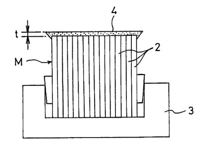
Fig. 7 is a schematic side view showing a state where a poly-
crystalline ~i-SiC plate is grown by the thermal chemical vapor
deposition method on crystal orientation faces of the plural
single crystal a-SiC pieces which are stacked and closely
contacted, Fig. 8 is a schematic side view showing a heat
treatment state of a complex, and Fig. 9 is an enlarged side
view of main portions and showing a state where single crystal
SiC is grown by a heat treatment.
CA 02269709 1999-04-23
_ g _
Best Mode for Carrying Out the Invention
Hereinafter, an embodiment will be described. Figs. 1 to
9 sequentially illustrate production steps of the method of
producing single crystal SiC according to the invention. In
Fig. l, 1 denotes a single crystal hexagonal a-SiC ingot (6H
type or 4H type) which is produced by the Achison method. As
shown by the arrow in Fig. 1, the single crystal a.-SiC ingot
1 has many plate-like single crystal SiC pieces lA of a wide
variety of sizes, and is provided with a feature that the
crystal orientation can be easily specified.
As shown in Figs. 2 and 3, thereafter, many plate-like
single crystal SiC pieces lA are cut out from the single crys-
tal a-SiC ingot 1. As shown in Figs. 4 and 5, from the plate-
like single crystal SiC pieces lA, rectangular plate-like
single crystal oc-SiC pieces 2 in which the length L of one
edge is about 1 cm and the thickness T is about 0.5 mm are
then cut out along the (110) crystal orientation faces 2a, and
the crystal orientation faces 2a are polished so that the
pieces are adjusted so as to have the same size.
As shown in Fig. 6, thereafter, a plurality, for example,
about 20 pieces of the single crystal oc-SiC pieces 2 which
are adjusted in size as described above are secured to a sin-
tered carbon jig 3 while they are arranged with setting their
crystal orientation faces 2a to be in a substantially same
plane and the faces of the C-axis direction, i.e., (0001)
CA 02269709 1999-04-23
- 10 -
faces are stacked and closely contacted with one another so
that the crystal orientations are unified into one direction.
The crystal orientation faces 2a of the plural single crystal
oc-SiC pieces 2 which are secured to the sintered carbon jig
3 are subjected to a grinding or polishing process so that
physical unevenness is eliminated.
More specifically, the crystal orientation faces 2a are
adjusted so as to have a surface roughness which is smaller
than 1,000 angstroms RMS, preferably, in the range of 100 to
500 angstroms RMS.
As shown in Fig. 7, thereafter, a (3-SiC plate 4 is formed
on the crystal orientation faces 2a of the plural single crys-
tal a-SiC pieces 2 which are stacked and closely contacted
with one another, by the thermal chemical vapor deposition
method (hereinafter, referred to as the thermal CVD method).
After the growth by the thermal CVD method, the surface of the
(3-SiC plate 4 is polished so that the thickness t becomes 300
to 700 Eun, preferably, about 500 E.um.
Next, carbon 5 is placed on the polished surface of the
~i-SiC plate 4 of a complex M consisting of the plural single
crystal oc-SiC pieces 2 and the j3-SiC plate 4. As shown in
Fig. 8, thereafter, under a state where the complex M is ac-
commodated in a carbon container 6 and the outer side of the
carbon container 6 is surrounded and covered with a-SiC pow-
der 7, the complex is heat-treated while it is held for about
CA 02269709 1999-04-23
- 11 -
20 hours at a temperature of 1,850 to 2,400~C, preferably,
2,200~C. As a result, as shown in Fig. 9, single crystal a-SiC
2' which is oriented in the same direction as the crystal axes
of the single crystal a-SiC pieces 2 is integrally grown from
each of the crystal orientation faces 2a of the single crystal
a-SiC pieces 2 toward the ~i-SiC plate 4.
The single crystal SiC which was produced by the above-
described production steps was cooled, and the surface of the
single crystal was then polished and etched by molten potas-
sium hydroxide (KOH). The surface was then magnified and ob-
served under a Nomarski microscope, with the result that no
grain boundary was found and etch pits in the same direction
as a hexagon were seen. From this, it was noted that single
crystal a-SiC was grown.
As described above, when the plural single crystal a-SiC
pieces 2 which are cut out into a rectangular plate like shape
from the single crystal ac-SiC ingot 1 produced by the Achison
method are used in a stacked and closely contacted state, the
crystal orientations of the plural single crystal a-SiC
pieces 2 can be easily specified into one direction. When the
complex M which is configured by forming the (3-SiC plate 4 on
the specified crystal orientation faces 2a is heat-treated,
the single crystals 21 a11 of which are grown at a high speed
toward the (3-SiC plate 4 with being oriented in the same di-
rection with respect to the crystal axes of the plural single
CA 02269709 1999-04-23
- 12 -
crystal SiC pieces 2 can be integrated by recrystallization
of polycrystals of the ~i-SiC plate 4. According to this con-
figuration, high-quality single crystal SiC in which crystal-
line nuclei, impurities, micropipe defects, and the like are
not generated in an interface, and which is thick can be effi-
ciently produced.
Particularly, it is preferable to adjust the crystal
orientation faces 2a of the plural single crystal a-SiC
pieces 2 by a grinding or polishing process so as to have a
surface roughness which is smaller than 1,000 angstroms RMS,
preferably, in the range of 100 to 500 angstroms RMS. The
employment of the adjustment of the surface roughness enables
high-quality single crystal SiC in which a mismatch of a crys-
tal lattice is eliminated and crystalline nuclei and the like
are not generated in an interface, to be obtained although
less process labor is consumed. Namely, physical unevenness
of the crystal orientation faces 2a of the single crystal oc-
SiC pieces 2 on which the ~i-SiC plate 4 is grown by the ther-
mal CVD method is preferably as small as possible because
crystalline nuclei are less generated. However, a process of
attaining a surface roughness which is smaller than 100 ang-
stroms RMS requires much labor and a long time period. When
the surface becomes rough or the surface roughness exceeds
1,000 angstroms RMS, phase transformation occurs simultane-
ously from a bottom face and a side face of a concave portion
CA 02269709 1999-04-23
- 13 -
in a heat treatment. Therefore, the possibility of eliminating
a mismatch of a crystal lattice is lowered, resulting in a
low-quality product in which crystalline nuclei are generated
in an interface.
Preferably, the [3-SiC plate 4 is polished so that the
thickness t after growth is 300 to 700 Eun, more preferably,
about 500 Eun. When the plate is polished after growth in this
way, a mismatch of a crystal lattice caused by lattice distor-
tion can be eliminated by a heat treatment for a relatively
short time period, and the productivity of single crystal SiC
of a higher quality can be improved. This will be described
below. When the (3-SiC plate 4 is a thick film which is thicker
than 700 Eun, phase transformation occurs during a heat treat-
ment while lattice distortion of the original crystal is main-
tained. In order to eliminate lattice distortion, therefore,
a heat treatment for a long term is required, thereby produc-
ing a fear that the productivity of single crystal SiC of a
higher quality is lowered. A mismatch of a crystal lattice
caused by lattice distortion in the crystal orientation faces
2a of the plural single crystal a-SiC pieces 2 which serve as
the foundation of the (3-SiC plate 4 tends to be suddenly
eliminated in the range of about 300 to 700 ~,un of the thick
ness from the single crystal a-SiC pieces. When the thickness
exceeds 700 Eun, the degree of elimination of a mismatch of a
crystal lattice is reduced.
CA 02269709 1999-04-23
- 14 -
In the heat treatment of the complex M, the surface of
the (3-SiC plate 4 after the growth is polished, the carbon 5
is placed on the polished surface, under a state where the
complex M is accommodated in the carbon container 6 and the
outer side of the carbon container 6 is surrounded and covered
with the a-SiC powder 7, the complex is subjected to a prede-
termined heat treatment. According to this configuration, the
a-SiC powder 7 is decomposed in a high-temperature atmos-
phere, and at least part of decomposed Si and C is moved into
the container 6 through the porous carbon container 6, so that
the predetermined heat treatment can be performed in a satu-
rated SiC vapor atmosphere. Accordingly, the decomposition of
the single crystal a-SiC pieces 2 and the ~i-SiC plate 4 can
be suppressed, whereby single crystal SiC of a high quality
can be produced and Si and C which are moved into the con-
tainer 6 through the porous carbon container 6 are prevented
from adhering to SiC before phase transformation. As a result,
it is possible to produce single crystal SiC which has a high
quality and is beautiful.
When steps of again grinding or polishing the surface of
the single crystal SiC which is produced as a result of the
above-mentioned steps, and forming the ~i-SiC plate 4 on the
polished surface by the thermal CVD method, and the heat
treatment of the complex M including the (3-SiC plate 4 are
repeated, it is possible to obtain single crystal SiC having
CA 02269709 1999-04-23
- 15 -
a large thickness along the crystal orientation. When stacked
single crystal oc-SiC pieces 2 are juxtaposed, the ~i-SiC plate
4 is formed on the whole area of the crystal orientation faces
2a of the group of the juxtaposed stacked single crystal oc-
SiC pieces 2 by the thermal CVD method, and the above-
mentioned heat treatment is then conducted, it is possible to
obtain single crystal SiC which is large also in the term of
area.
In the embodiment, the plate-like single crystal a-SiC
pieces 2 are used as the single crystal SiC pieces. Alterna-
tively, for example, plate-like crystal pieces such as a-SiC
sintered members or single crystal ~i-SiC members may be used.
In the embodiment, the crystalline (3-SiC plate 2 which is
grown on the crystal orientation faces 2a of the plural single
crystal a-SiC pieces 2 by the thermal CVD is used as the
polycrystalline plate. Alternatively, for example, a polycrys-
talline oc-SiC plate, an SiC sintered member of high purity,
or an amorphous plate of high purity (lOl4ar~~~3~ or less may
be used, and it is possible to obtain single crystal SiC of
a high quality in the same manner as the embodiment.
As the single crystal a-SiC pieces 2 in the embodiment,
either of the 6H type or the 4H type may be used. When the
6H type is used, a single crystal which is converted from
polycrystals of the polycrystalline (3-SiC plate 2 into a-SiC
as the progress of the heat treatment is easily grown in the
CA 02269709 1999-04-23
- 16 -
same form as that of a single crystal of the 6H type. When
single crystal pieces of the 4H type are used, a single crys-
tal in the same form as that of a single crystal of the 4H
type is easily converted and grown.
Industrial Applicability
As described above, the invention is a technique that a
complex in which a polycrystalline plate consisting of Si and
C atoms is stacked on crystal orientation faces of plural
plate-like single crystal SiC pieces that are stacked and
closely contacted while crystal orientations are unified into
one direction is subjected to heat treatment, so that a single
crystal which is oriented in the same direction as the crystal
axes of the single crystal pieces is integrally grown from the
crystal orientation faces of the single crystal SiC pieces
toward the polycrystalline plate, whereby high-quality single
crystal SiC in which crystalline nuclei, impurities, micropipe
defects, and the like are not generated in an interface, and
which is thick can be efficiently produced.