Note: Descriptions are shown in the official language in which they were submitted.
CA 02269856 1999-04-26
WO 98I19350 PCT/US97/19253
COMPOSITE MEMORY MATERIAL COMPRISING A MIXTURE OF PHASE
CHANGE MEMORY MATERIAL AND DIELECTRIC MATERIAL
FIELD OF THE INVENTION
The present invention relates generally to electrically operated memory
material. More specifically, the present invention relates to a composite
memory
material comprising a mixture of active phase-change memory material and
inactive dielectric material.
BACKGROUND AND PRIOR ART
The Ovonic EEPROM is a novel, proprietary, high performance, non-volatile,
thin-film electronic memory device. Its advantages include non-volatile
storage of
data, potential for high bit density and, consequently, low cost because of
its small
footprint and simple two-terminal device configuration, long reprogramming
cycle
life, low programming energies and high speed. The Ovonic EEPROM is capable
of both analog and digital forms of information storage. Digital storage can
be
either binary (one bit per memory cell) or multi-state (multiple bits per
cell). Only
minor modifications are necessary to switch between the two digital modes. For
purposes of the instant invention, the terms "memory elements" and "control
2o elements" will be employed synonymously.
EARLY ELECTRICAL PHASE CHANGE MEMORY
The general concept of utilizing electrically writable and erasable phase
change materials (i.e., materials which can be electrically switched between
generally amorphous and generally crystalline states) for electronic memory
applications is well known in the art, as is disclosed, for example, in U.S.
Patent
No. 3,271,591 to Ovshinsky, issued September 6, 1966 and in U.S. Patent No.
3,530,441 to Ovshinsky) issued September 22, 1970, both of which are assigned
to the same assignee as the present invention, and both disclosures of which
are
incorporated herein by reference (hereinafter the "Ovshinsky patents").
As disclosed in the Ovshinsky patents, such phase change materials can
be electrically switched between structural states of generally amorphous and
generally crystalline local order or between different detectable states of
local order
CA 02269856 1999-04-26
WO 98/19350 PCT/US97/19253
2
across the entire spectrum between completely amorphous and completely
crystalline states. That is, the Ovshinsky patents describe that the
electrical
switching of such materials is not required to take place between completely
amorphous and completely crystalline states but rather can be in incremental
steps
reflecting changes of local order to provide a "gray scale" represented by a
multiplicity of conditions of local order spanning the spectrum between the
completely amorphous and the completely crystalline states. The early
materials
described by the Ovshinsky patents could also, if required, be switched
between
just the two structural states of generally amorphous and generally
crystalline local
1 o order to accommodate the storage and retrieval of single bits of encoded
binary
information.
The electrically erasable phase change memories described in the
Ovshinsky patents, as well as subsequent electrical solid state memory, had a
number of limitations that prevented their widespread use as a direct and
universal
replacement for present computer memory applications, such as tape, floppy
disks,
magnetic or optical hard disk drives, solid state disk flash, DRAM, SRAM, and
socket flash memory. Specifically, the following represent the most
significant of
these limitations: (i) a relatively slow (by present standards) electrical
switching
speed, particularly when switched in the direction of greater local order (in
the
2o direction of increasing crystallization); (ii) a relatively high input
energy requirement
necessary to initiate a detectable change in local order; and (iii) a
relatively high
cost per megabyte of stored information (particularly in comparison to present
hard
disk drive media).
The most significant of these limitations is the relatively high energy input
required to obtain detectable changes in the chemical andlor electronic
bonding
configurations of the chalcogenide material in order to initiate a detectable
change
in local order. Also significant were the switching times of the electrical
memory
materials described in the Ovshinsky patents. These materials typically
required
times in the range of a few milliseconds for the set time (the time required
to
3o switch the material from the amorphous to the crystalline state); and
approximately
a microsecond for the reset time (the time required to switch the material
from the
crystalline back to the amorphous state). The electrical energy required to
switch
CA 02269856 1999-04-26
WO 98/19350 PCT/US97/19253
3
these materials typically measured in the range of about a microjoule.
It should be noted that this amount of energy must be delivered to each of
the memory elements in the solid state matrix of rows and columns of memory
cells. Such high energy levels translate into high current carrying
requirements for
the address lines and for the cell isolationladdress device associated with
each
discrete memory element. Taking into consideration these energy requirements,
the choices of memory cell isolation elements for one skilled in the art would
be
limited to very large single crystal diode or transistor isolation devices,
which would
make the use of micron scale lithography and hence a high packing density of
1o memory elements impossible. Thus, the low bit densities of matrix arrays
made
from this material would result in a high cost per megabyte of stored
information.
By effectively narrowing the distinction in price and performance between
archival, non-volatile mass memory and fast, volatile system memory, the
memory
elements of the present invention have the capability of allowing for the
creation
of a novel, non-hierarchal "universal memory system". Essentially all of the
memory in the system can be low cost, archival and fast. As compared to
original
Ovshinsky-type phase change electrical memories, the memory materials
described
herein provide over six orders of magnitude faster programming time {less than
30
nanoseconds) and use extremely low programming energy (less than 0.1 to 2
nanojoules) with demonstrated long term stability and cyclability (in excess
of 10
trillion cycles). Also, experimental results indicate that additional
reductions in
element size can increase switching speeds and cycle life.
In general, development and optimization of the class of chalcogenide
memory materials has not proceeded at the same rate as other types of solid
state
electrical memories that now have substantially faster switching times and
substantially lower set and reset energies. These other forms of memories
typically employ one or two solid state microelectronic circuit elements for
each
memory bit (as many as three or four transistors per bit) in some memory
applications. The primary "non-volatile" memory elements in such solid state
3o memories, such as EEPROM, are typically floating gate field effect
transistor
devices which have limited re-programmability and which hold a charge on the
gate
of a field effect transistor to store each memory bit. Since this charge can
leak off
CA 02269856 1999-04-26
WO 98I19350 PCT/US97/19253
4
with the passage of time, the storage of information is not truly non-volatile
as it
is in the phase change media of the prior art where information is stored
through
changes in the actual atomic configuration or electronic structure of the
chalcogenide material from which the elements are fabricated. These other
forms
of memories now enjoy acceptance in the marketplace.
In contrast to DRAM and SRAM, volatile memory devices, and other "flash"
devices such as floating gate structures, no field effect transistor devices
are
required in the electrical memory devices of the present invention. In fact,
the
electrically erasable, directly overwritable memory elements of the present
invention represent the simplest electrical memory device to fabricate,
comprising
only two electrical contacts to a monolithic body of thin film chalcogenide
material
and a semiconductor diode for isolation. As a result, very little chip "real
estate"
is required to store a bit of information, thereby providing for inherently
high density
memory chips. Furthermore, additional increases in information density can be
accomplished through the use of multibit storage in each discrete memory cell.
In order to address the flash EEPROM market and be considered as a
universal memory, memory elements must be truly non-volatile. This is even
more
significant if the memory element is claimed to possess multibit storage
capabilities. If a set resistance value is lost or even found to significantly
drift over
time, the information stored therein is destroyed, users Pose confidence in
the
archival capabilities of the memory.
In addition to set resistance stability, another highly important factor which
would be required of a universal memory is low switching current. This is
extremely significant when the EEPROMs are used for large scale archival
storage.
Used in this manner) the EEPROMs would replace the mechanical hard drives
(such as magnetic or optical hard drives) of present computer systems) One of
the
main reasons for this replacement of conventional mechanical hard drives with
EEPROM "hard drives" would be to reduce the comparatively large power
consumption of the mechanical systems. In the case of lap-top computers, this
is
of particular interest because the mechanical hard disk drive is one of the
largest
power consumers therein. Therefore) it would be especially advantageous to
reduce this power load, thereby substantially increasing the usage time of the
CA 02269856 1999-04-26
WO 98I19350 PCT/US97/19253
computer per charge of the power cells. However, if the EEPROM replacement
for mechanical hard drives has high switching energy requirements (and
therefore
high power requirements), the power savings may be inconsequential or at best
unsubstantial. Therefore, any EEPROM which is to be considered a universal
5 memory requires low switching energy.
Yet another requirement of a EEPROM universal memory is high thermal
stability of the information stored therein. Today's computers, especially
personal
computers, are routinely subjected to high temperatures. These high
temperatures
can be caused by internally created heat such as from power sources or other
heat
producing internal components. These high temperatures may also be caused by
environmental factors, such as use of the computer in a hot climate or storage
of
the computer in an environment which is directly or indirectly heated to
higher than
normal temperatures. Whatever the cause of the elevated temperatures, present
computer memory systems, especially "hard" or archival memory, must be
thermally stable even at relatively high temperatures. Without this thermal
stability
data loss may occur leading to the aforementioned loss of credibility.
Still another requirement of a EEPROM universal memory is long
write/erase cycle life. For EEPROMs, as is the case with all archival memory,
cycle life plays an important role in consumer confidence and acceptance. If
the
2o cycle life of a memory device is too short, the consumer will be adverse to
using
this device for fear of losing valuable data. If the EEPROM is to be used as a
replacement for computers main memory or display memory, that is, as a
replacement for DRAM, SRAM or VRAM, the requirement of long cycle life is even
more critical. The main and display memory are a computer's most often written
to/erased data storage area. Every time a new computer program is loaded; a
portion of the computer's main memory is erased and rewritten. During the
execution of a computer program, a portion of the computer's main memory is
constantly being cycled. Every time the computer monitor's display is changed,
portions of the display memory are cycled. If the EEPROMs used to replace the
3o computer's main and display memory do not have a relatively long
writelerase
cycle life, these memories would need to be replaced excessively.
CA 02269856 1999-04-26
WO 98I19350 PCT/US97/19253
6
SUMMARY OF THE INVENTION
An object of the present invention is to provide a solid state memory
material having reduced switching current requirements and greater thermal
stability of stored data therein. It is also an object of the present
invention to
provide a memory element comprising the aforementioned memory material.
These and other objects of the present invention are accomplished by a
composite memory material comprising: a mixture of active phase-change memory
material and inactive dielectric material. The phase-change memory material
includes one or more elements selected from the group consisting of Te, Se,
Ge,
Sb, Bi, Pb, Sn, As, S, Si, P) 0 and mixtures or alloys thereof.
These and other objects are also accomplished by a single cell memory
element comprising: a volume of memory material defining a single cell memory
element, the memory material comprising a mixture of active phase-change
material and inactive dielectric material; and a pair of spacedly disposed
contacts,
the contacts providing terminals for reading information stored in and writing
information to the memory element.
There and other objects are also accomplished by an electrically operated,
directly overwritable, multibit, single cell memory element comprising: a
volume of
memory material defining a single cell memory element, the memory material
2o constituting means for assuming a large dynamic range of electrical
resistance
values with the ability to be set directly to one of a plurality of resistance
values
within the dynamic range without the need to be set to a specific starting or
erased
resistance value, regardless of the previous resistance value of the material
in
response to a selected electrical input signal so as to provide the single
cell with
multibit storage capabilities; and a pair of spacedly disposed contacts for
supplying
the electrical input signal to set the memory material to a selected
resistance value
within the dynamic range, wherein at least one of the spacedly disposed
contacts
is a mixture of a first contact material and a second contact material,
wherein the
first contact material includes carbon, and wherein the second contact
material
includes at least one transition metal element. Preferably, the second contact
material includes one or more elements selected from the group consisting of
Ti,
V, Cr, Zr, Nb, Mo, Hf) Ta, W and mixtures or alloys thereof. More preferably,
the
CA 02269856 1999-04-26
WO 98/19350 PCT/US97/19253
7
second contact material includes Ti and W.
BRIEF DESCRIPTION OF THE DRAWINGS
Figure 1 is a cross-sectional view of a single memory element depicting the
composite memory material and pair of contacts;
Figure 2 is the top view of a possible layout of multiple memory elements
showing how the elements would be connected to a set of X-Y addressing lines;
Figure 3 is a schematic diagram of the memory elements from Fig. 1
showing, in addition, how isolation elements such as diodes are connected in
1o series with the memory elements to electrically isolate each of the devices
from the
others; and
Figure 4 is a schematic representation illustrating a single crystal
semiconductor substrate with the integrated memory matrix of the instant
invention
as depicted in Figure 1 placed in electrical communication with an integrated
circuit
chip on which the address/driversldecoders are operatively affixed.
DETAILED DESCRIPTION OF THE INVENTION
Disclosed herein is a composite memory material comprising a mixture of
phase-change memory material and inactive dielectric material. The composite
2o memory material of the present invention provides for switching within a
wide
dynamic range of stable states with low energy inputs at fast speeds so that
it can
be used to fabricate improved electrical memory elements.
The composite memory material is non-volatile and will maintain the integrity
of stored information (within a selected margin of error) without the need for
periodic refresh signals. The composite memory material can also be directly
ovenrvritable so that the discrete memory elements need not be erased (set to
a
specified starting point) in order to change the information stored there. The
fast
and low energy switching to any of the different values of resistance can be
attributed to the fact that the switching occurs without the need for gross
atomic
3o rearrangement of the phase-change switching material.
As stated, the composite memory material is a mixture of active phase-
change memory material and inactive dielectric material. The active phase-
change
CA 02269856 1999-04-26
WO 98/19350 PCT/US97/19253
8
memory material is formed from a plurality of constituent atomic elements. The
phase-change memory material includes one or more elements selected from the
group consisting of Te, Se, Ge, Sb, Bi, Pb, Sn, As, S, Si, P, O and mixtures
or
alloys thereof. The phase-change memory material preferably includes at least
one chalcogen element and may include at least one transition metal element.
Preferably, the chalcogen element is selected from the group consisting of
Te, Se and mixtures or alloys thereof. More preferably, the chalcogen element
is
a mixture of Te and Se.
The term "transition metal" as used herein includes elements 21 to 30, 39
to 48, 57 and 72 to 80. Preferably, the transition metal element is selected
from
the group consisting of Cr) Fe, Ni, Nb, Pd, Pt and mixtures or alloys thereof.
Most
preferably the transition metal is Ni. Specific examples of such multi-element
systems are set forth hereinafter with respect to the Te:Ge:Sb system with or
without Ni and/or Se.
Specifically, the tellurium alloys described herein have a valence band made
up of lone pair states. Since four (4) p shell electrons are present in Te,
and the
Te atom is chemically bonded by two of these bonding electrons in the p shell,
the
other two outer electrons (the lone pair) are not utilized for bonding
purposes and
hence do not substantially change the atomic energy of the system. In this
regard,
note that the highest filled molecular orbital is the orbital which contains
the lone
pair electrons. This is significant because, in a pertect stoichiometric
crystal of
tellurium and germanium atoms, upon the application of some internal strain in
the
lattice from which the crystallite is formed, the valence band can broaden and
move upward toward the position of the then existing Fermi level. However,
TeGe
crystals are naturally "self-compensated", that is, the crystal desires ~ to
preferentially assume a Te rich (approximately 52 percent Te and 48 percent
Ge)
composition. The stoichiometric crystal is a face centered cube; however, with
the
addition of a minimal amount of energy, the crystal can assume a rhombohedral
lattice structure by increasing the number of its Ge and/or Sb vacancies. It
is this
3o creation of vacancies in the crystalline lattice structure, which can
reduce lattice
strain in TeGe alloys, is responsible for lowering the energy state of the
material
and moves the Fermi level toward the valence band.
CA 02269856 1999-04-26
WO 98I19350 PCT/US97119253
9
1t is acceptable, if not essential to superimpose an amorphous model of
local order on top of a short range local order model for the purpose of
obtaining
a descriptive, if not pertectly predictive explanation of atomic behavior.
When
considering the amorphous nature of the material, note that the density of
defect
states in the band tails is greatest adjacent the band edges, while the depth
of the
recombination centers for captured charge carriers are deeper farther away
from
the band edges. The presence of these deep traps and tail states would provide
a possible explanation for intermediate stable resistance values between the
Fermi
level position and the band edge. Regardless of theory, when fully
crystalline, the
semiconductor material of the instant invention is a degenerate semiconductor
which exhibits metallic-like conduction.
It is further believed that the size of the crystallites which exist in the
bulk
of the semiconductor and memory material is relatively small, preferably less
than
about 2000 ~, more preferably between about 50 ~ and 500 A, and most
preferably
on the order of about 200 A to about 400 A. Further, these crystallites are
believed
to be surrounded by an amorphous skin which may contribute to the rapid
formation of the many Fermi level positions of the material) detectable as
different
resistances (conductivities), as well as to the lower energy requirements for
the
transitions between these detectable resistance values to which the material
can
2o be reliably and repeatably set.
It has also been found that modulation of the switching characteristics of two
or three terminal semiconductor devices fabricated from the microcrystalline
materials of the present invention may be controlled such that repeatable and
detectable resistance values can be effected. It has been found that, in order
for
the materials of the present invention to be quickly set by low energy input
signals
to a desired conductivity (determined by the Fermi level position), it is only
necessary that said materials are capable of stable (or long lived metastable)
existence within at least two different Fermi level positions, which Fermi
level
positions are characterized by substantially constant band gaps but different
electrical cond,uctivities. As noted above) it is also believed that the
relatively small
crystallite size may contribute to the rapid transition between detectable
values of
resistance.
CA 02269856 1999-04-26
WO 98/19350 PCT/US97/19253
One characteristic of the semiconductor materials of the present invention
is their tendency toward the formation of more and smaller crystallites per
unit
volume. Crystallite sizes of the widest preferential range of representative
materials embodying the present invention have been found to be far less than
5 about 2000 /~, and generally less than the range of about 2,000 A to 5,000 ~
which
was characteristic of prior art materials. Crystallite size is defined herein
as the
diameter of the crystallites, or of their "characteristic dimension" which is
equivalent to the diameter where the crystallites are not spherically shaped.
It has been determined that compositions in the highly resistive state of the
10 class of TeGeSb materials which meet the criteria of the present invention
are
generally characterized by substantially reduced concentrations of Te relative
to
that present in prior art electrically erasable memory materials. In one
composition
that provides substantially improved electrical switching pertormance
characteristics, the average concentration of Te in the as deposited materials
was
well below 70%, typically below about 60% and ranged in general from as low as
about 23% up to about 58% Te and most preferably about 48% to 58% Te.
Concentrations of Ge were above about 5% and ranged from a low of about 8%
to about 30% average in the material, remaining generally below 50%. Most
preferably, concentrations of Ge ranged from about 8% to about 40%. The
2o remainder of the principal constituent elements in this composition was Sb.
The
percentages given are atomic percentages which total 100% of the atoms of the
constituent elements. Thus, this composition may be characterized as
TeaGebSb,~o.~9+b~. These ternary Te-Ge-Sb alloys are useful starting materials
for
the development of additional phase-change memory materials having even better
electrical characteristics.
The phase-change memory material preferably includes at least one
chalcogen and can include one or more transition metals. The phase-change
materials which include transition metals are elementally modified forms of
the
phase-change materials in the Te-Ge-Sb ternary system. That is, the
elementally
modified phase-change materials constitute modified forms ofthe Te-Ge-Sb phase-
change alloys. This elemental modification is achieved by the incorporation of
transition metals into the basic Te-Ge-Sb ternary system, with or without an
CA 02269856 1999-04-26
WO 98/19350 PCT/US97/19253
11
additional chalcogen element, such as Se. Generally the elementally modified
phase-change materials fall into two categories.
The first category is a phase-change memory material which includes Te,
Ge, Sb and a transition metal, in the ratio (TeaGeeSb,oo-~a+n>)~TM,oo-~ where
the
subscripts are in atomic percentages which total 100% of the constituent
elements,
wherein TM is one or more transition metals, a and b are as set forth herein
above
for the basic Te--Ge--Sb ternary system and c is between about 90% and about
99.99%. The transition metal preferably include Cr, Fe) Ni, Nb, Pd, Pt and
mixtures
or alloys thereof.
Specific examples of phase-change memory materials encompassed by this
system would include (TeSSGezzSb2z)95N~5. (TeSSGez2Sb22)s~Ni,~,
(Te56Gez2Sbz2)95Cr5,
(TeSSGezzsbzz)soCr~o, (TeSSGezzSbzz)s5Fe5, (TessGezzsbzz)soFe,o,
~TeSSGezzS~zz)s5Pd5,
(TeSSGezzsbzz)soPd,o~ (Te5sGe2zSbz2)ssPts, (TessGezzSbzz)ssPt~o,
(TeSSC'ezzSbzz)s5Nb5~
(TeSSGezzSbzz)soNb,o~ ~Tess~''ezzSb2z)soN~5Cr5~ (Te5sGe2zSb2z)soNi5Fe5,
(TeSSGeZZSbZZ)soCrSFes, (TeSSGezzSbzZ)soPd5Cr5, (TeSSGezzSb2z)soNi5Pd5,
(Te56GeZZSbZZ)soPd5Pt5, etC.
The second category is a phase-change memory material which includes
Te, Ge, Sb, Se and a transition metal, in the ratio
(TeaGebSb,oo-ca+by~TMaSe,oo-o+d~ where the subscripts are in atomic
percentages
which total 100% of the constituent elements, TM is one or more transition
metals,
a and b are as set forth hereinabove for the basic Te-Ge-Sb ternary system, c
is
between about 90% and 99.5% and d is between about 0.01 % and 10%. The
transition metal can preferably include Cr, Fe, Ni, Pd, Pt, Nb and mixtures or
alloys
thereof. Specific examples of memory materials encompassed by this system
would include (TeSSGezzSbzz)soNi5Se5, (TeSSGezzSbZZ)BONi~oSe-~o,
(TeSBGeZ2Sb22)90Cr5Se5, (TeSSGezzSbzz)soCr,ose,o~ (TeSSGezzSb2z)soFe5Se5,
(TeSSGezzSb2x)aoFe,oSe,o~ (TeSSGez2Sbzz)soPdsSeS, (TeSSGezzsbzz)soPd~ose,o~
(TeSSGezzsbzz)soPtSSes, (TeSSGezzsbzz)aoPt,ose,o~ (TeSSGezzSbzz)soNb5Se5,
(TeSSGezzsbzz)aoNb,oSe,o, (Te56Ge22~b22)85N~5Cr5Se5~
(TeSSGezzSbzz)aoNisFeSSe,o,
(TeSSGeZZSb22)asCr5Fe5Se5,
(Te5sGe2zSbzz)a5Ni5Pd5Se5,(Te5sGe22Sb22)aoNi5Pt5Se~o)
(Te5sGe22sbzz)s5Ni5Nb5Se5, (TessGe2zSb22)s5Pd5Cr5Se5,
(TeSSGezzsbzz)eoPd5Pt5Se,o,
(Te56Gez2Sb22)sSPdsNb5Se5, (Te56Ge2zSbz2)s5Pt5Nb5Se5, etc.
CA 02269856 1999-04-26
WO 98/19350 PCT/US97/19253
12
The phase-change memory material possesses substantially non-volatile set
resistance values. However, if the resistance value of the phase-change
material
does drift from its original set value, "compositional modification",
described
hereinafter, may be used to compensate for this drift. As used herein, the
term
"non-volatile" refers to the condition in which the set resistance value
remains
substantially constant for archival time periods. Of course, software
(including the
feedback system discussed hereinafter) can be employed to insure that
absolutely
no "drift" occurs outside of a selected margin of error. Because drift of the
resistance value of the memory elements can, if left unimpeded, hinder gray
scale
storage of information, it is desirable to minimize drift.
"Compositional modification" is defined herein to include any means of
compositionally modifying the phase-change memory material to yield
substantially
stable values of resistance, including the addition of band gap widening
elements
to increase the inherent resistance of the material. One example of
compositional
modification is to include graded compositional inhomogeneities with respect
to
thickness. For instances, the volume of phase-change memory material may be
graded from a first Te-Ge-Sb alloy to a second Te-Ge-Sb alloy of differing
composition. The compositional grading may take any form which reduces set
resistance value drift. For example, the compositional grading need not be
limited
to a first and second alloy of the same alloy system. Also, the grading can be
accomplished with more than two alloys. The grading can be uniform and
continuous or it can also be non-uniform or non-continuous. A specific example
of compositional grading which results in reduced resistance value drift
includes
a uniform and continuous grading of Ge,4Sb29Te5, at one surtace to
GeZZSb2ZTess
at the opposite surtace.
Another manner of employing compositional modification to reduce
resistance drift is by layering the volume of phase-change memory material.
That
is, the volume of phase-change memory material may be formed of a plurality of
discrete, relatively thin layers of differing composition. For example, the
volume
of phase-change memory material may include one or more pairs of layers, each
one of which is formed of a different Te-Ge-Sb alloy. Again, as was the case
with
graded compositions, any combination of layers which results in substantially
CA 02269856 1999-04-26
WO 98I19350 PCT/US97/19253
13
reduced resistance value drift can be employed. The layers may be of similar
thickness or they may be of differing thickness. Any number of layers may be
used and multiple layers of the same alloy may be present in the volume of
memory material, either contiguous or remote from one another. Also, layers of
any number of differing alloy composition may be used. A specific example of
compositional layering is a volume of memory material which includes
alternating
layer pairs of Ge,4Sbz9Te5, and Ge22Sbz2Te56.
Yet another form of compositional inhomogeneity to reduce resistance drift
is accomplished by combining compositional grading and compositional layering.
More particularly, the aforementioned compositional grading may be combined
with
any of the above described compositional layering to form a stable volume of
memory material. Exemplary volumes of phase-change memory material which
employ this combination are: (1 ) a volume of phase-change memory material
which includes a discrete layer of Ge22Sb22Te56 followed by a graded
composition
of Ge,4Sb29Te5~ and Ge2ZSbZZTe56 and (2) a volume of phase-change memory
material which includes a discrete layer of Ge,4Sb29Te5, and a graded
composition
Of Ge~4SbZ9Te5~ and Ge22Sb22Te56.
The composite memory material is a mixture of an active phase-change
memory material, such as those described above, and an inactive dielectric
2o material. Generally, the dielectric material can be any dielectric material
that is
chemically non-reactive with the phase-change memory material. Preferably, the
dielectric material has a melting point higher than that of the phase-change
memory material.
In particular, the dielectric material may be one or more materials selected
from the group consisting of oxides, nitrides, fluorides, sulfides, chlorides,
carbides,
oxynitrides, carboxynitrides, borides, phosphides and mixtures or alloys
thereof.
Other dielectric materials known in the art may also be used. The dielectric
material may also be chosen from the group of organic dielectric materials.
These
include, but are not limited to, materials such as amides, polyamides, imides,
polyimides, and parylens.
Oxides include silicon oxides such as Si02, titanium oxides such as TiOz,
aluminum oxides such as AIz03, zirconium oxides such as Zr02, germanium oxides
CA 02269856 1999-04-26
WO 98I19350 PCT/US97/19253
14
such as GeOZ, and tatalum oxides such as Ta205. Other possible oxides include
B203, Sb203, and PbO. Nitrides include silicon nitrides such as Si3N4,
aluminum
nitrides such as AIN, as well as TiN, SiN, ZrN and BN, and off-stoichiometry
silicon
nitride SiNx. Sulfides include silicon sulfide such as SiSz, germanium sulfide
such
as GeSz, and zinc sulfide such as ZnS. Florides include MgF2, CaFz, and LiFz.
Various glasses may also be used. For instance, LaSiON material
containing La, Si, O and N; SiAION material containing Si, AI, O and N; SiAION
material containing yttrium; or NdSiON material containing Nd) Si, O and N may
be used.
1o The composite memory material is preferably a heterogeneous mixture of
active phase-change memory material and inactive dielectric material. One
embodiment of such a heterogeneous mixture is that of a multi-layered
structure
with layers of phase-change memory material intermixed with layers of
dielectric
material. Preferably, the thickness of each layer may be between about 5 A to
about 75 A. More preferably, the thickness of each layer may be between about
10 ~ to about 50 /~. Most preferably, the thickness of each layer may be
between
about 20 ~ to about 30 ~.
The composite memory material may be made by methods such as
sputtering, evaporation or by chemical vapor deposition (CVD), which may be
enhanced by plasma techniques such as RF glow discharge. The composite
memory material of the instant invention is most preferably made by RF
sputtering
or evaporation. It may be formed by multiple source sputtering techniques
making
use of a plurality of targets, usually a target of the phase-change memory
material
and a target of the dielectric material. With these targets arranged in
opposition
to a substrate, sputtering is carried out while the substrate is rotated
relative to
each target. A target containing both phase change and dielectric materials
may
be used as well. As well, substrate heating may be used to control the
morphology of the phase-change material within the composite memory material
formed by affecting crystal growth as well as crystal aggregation via surtace
mobility.
The percentage by volume of dielectric material within the composite
memory material can be controlled. Preferably, the percentage by volume of
CA 02269856 1999-04-26
WO 98/19350 PCT/US97/19253
dielectric material is between about 10% and about 90%. More preferably, the
percentage by volume of dielectric material is between about 20% and about
80%.
Most preferably, the percentage by volume of dielectric material is between
about
40% and about 60%.
5 The composite memory material may also be formed by a spin coating
process. The phase-change memory material may be mixed with a dielectric such
as an organic polymer like polyamide. The resulting mixture may then be spin
coated onto a silicon substrate forming a composite memory material with the
desired properties.
10 Also disclosed herein is a single cell memory element comprising the
composite memory material disclosed above. The memory element further
comprises a pair of speacedly disposed contacts for supplying the electrical
input
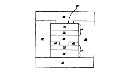
signal to the composite memory material. Figure 1 shows a cross-sectional view
of an embodiment of the memory element formed on a single crystal silicon
15 semiconductor wafer 10. The memory element includes the composite memory
material 36, a first spacedly disposed contact 6, and a second spacedly
disposed
contact 8.
First contact 6 and second contact 8 may each be comprised of two thin-film
layers. Thin-film layers 38 and 34, deposited adjacent to the composite memory
material 36 have excellent diffusion barrier properties which inhibit the
diffusion and
electromigration of foreign material into the composite memory material 36.
The adjacent thin-film layers 38, 34 may be comprised of a carbon material
such as amorphous carbon. Alternately, the adjacent thin-film layers 38) 34
may
be formed from a compound which includes one element selected from the group
consisting of Ti, V, Cr, Zr) Nb, M. Hf, Ta, W, and one or more elements
selected
from the group consisting of B, C, N, AI, Si, P, S. Preferably, the adjacent
thin-film
layers 38, 34 are formed from a compound which includes Ti and one or more
elements selected from the group consisting of C, N, AI, Si and mixtures or
alloys
thereof. In one embodiment, the adjacent thin-film layers are comprised of a
compound having a composition of, in atomic percent, between about 10% to 60%
titanium, 5% to 50% caFbon and 10% to 60% nitrogen. In addition, the titanium
carbonitride may also include up to 40% hydrogen.
CA 02269856 1999-04-26
WO 98/19350 PCT/US97/19253
16
In another embodiment, the adjacent thin-film layers 38, 34 are comprised
of titanium siliconitride. Preferably, in this embodiment, the adjacent thin-
film
layers are comprised of a compound having a composition of, in atomic percent,
between about 10% to 60% titanium, 5% to 50% silicon and 10% to 60% nitrogen.
In addition, the titanium siliconitride may also include up to 40% hydrogen.
In a third embodiment, the adjacent thin-film layers 38, 34 are comprised of
titanium aluminum nitride. Preferably, in this embodiment, the adjacent thin-
film
layers are comprised of a compound having a composition of, in atomic percent,
between about 10% to 60% titanium, 5% to 50% aluminum and 10% to 60%
1o nitrogen. In addition, the titanium aluminum nitride may also include up to
40%
hydrogen.
The titanium carbonitride, titanium siliconitride and titanium aluminum
nitride
have excellent barrier properties, preventing both the diffusion and
electromigration
of foreign material into the composite memory material. Furthermore, the
titanium
carbonitride, titanium siliconitride and titanium aluminum nitride may be
deposited
by such methods as physical vapor deposition including evaporation, ion
plating
as well as DC and RF sputtering deposition, chemical vapor deposition, and
plasma assisted chemical vapor deposition. The exact method used depends
upon many factors, one of which being deposition temperature constraints
imposed
2o by the composition of the target material.
The pair of spacedly disposed contacts 6 and 8 are preferably comprised
of the additional thin-film layers 32 and 40 which are deposited remote to the
composite memory material 3fi. Each of these remote thin-film layers is
comprised
of one or more elements from the group consisting of Ti, W and Mo. In one
embodiment, each of the remote thin-film layers is comprised of Ti and W.
Preferably, the remote thin-film layers are comprised of a compound, in atomic
percent, of 5% to 30% titanium and 70% to 95% tungsten. The Ti-W alloy layers
32 and 40 are preferably deposited using a DC sputtering deposition process.
They are preferably deposited to a thickness of about 100 /~ to 4000 ~. They
are
more preferably deposited to a thickness of about 200 A to 2000 A. The Ti-W
alloy
layers 32 and 40 have excellent ohmic contact proterties. Moreover, they have
the
barrier properties necessary to prevent both the electromigration and
diffusion of
CA 02269856 1999-04-26
WO 98/19350 PCT/US97/19253
17
foreign electrode material into the composite memory material 36.
The layer of composite memory material 36 is preferably deposited to a
thickness of about 200 ~ to 5,000 ~, more preferably of about 250 ~ to 2,500
~,
and most preferably of about 250 ~ to 500 l~ in thickness.
The memory element shown in Figure 1 may be formed in a multi-step
process. Layers 32) 34 and 46 are first deposited and the insulation layer 46
is
then etched so that there will be an area of contact between the composite
memory material 36 and layer 34. The remaining layers 36, 38 and 40 are
deposited and the entire stack of layers 32, 34, 36, 46, 38 and 40 is etched
to the
selected dimension. Deposited on top of the entire structure is a layer of
insulating
material 39. Examples of insulating materials are Si02, Si3N4 and tellurium
oxygen
sulfide (e.g., TeOS). The layer of insulating material 39 is etched and a
layer of
aluminum is deposited to form the second electrode grid structure 42 which
extends perpendicular in direction to the conductors 12 and complete the X-Y
grid
connection to the individual memory elements. Overlaying the complete
integrated
structure is a top encapsulating layer of a suitable encapsulant such as Si3N4
or
a plastic material such as polyamide, which seals the structure against
moisture
anal other external elements which could cause deterioration and degradation
of
performance. The Si3N4 encapsulant can be deposited, for example, using a low
temperature plasma deposition process. The polyamide material can be spin
coated and baked after deposition in accordance with known techniques to form
the encapsulant layer.
The term "pore diameter" as used herein is the average cross-section of the
smallest region of contact between the composite memory material 36, and the
electrical contacts 6 and 8. The pore diameter can be as small as lithography
resolution limits will permit. Pore diameter is related to device pertormance.
Reducing pore diameter reduces device volume, thereby lowering the current and
energy requirements needed for electrical switching. This increases the speed
and sensitivity of the device - reducing the switching time and electrical
energy
required to initiate the detectable change in resistance.
In previous embodiments of the memory element it was preferred that the
pore diameter be selected to conform substantially with the cross section of
the
CA 02269856 1999-04-26
WO 98I19350 PCT/US97/19253
18
memory material whose resistance is actually altered when the material is
switched
to either the high or low resistance state. This section of memory material is
called
the "filamentary portion". Ideally, the pore diameter should equal the
diameter of
the filamentary portion.
As a means of reducing pore diameter beyond that permitted by lithography,
previous embodiments of the memory element have employed "filament confining
means" between at least one of the saacedlv disposed contacts and the volume
of memory material. The filament confining means is, typically, a thin-film
layer of
highly resistive material with at least one low resistance pathway thereacross
through which current passes between the electrical contact and the volume of
memory material. The filament confining means provided a high current density
within the filamentary portion upon input of a very low electrical current to
the
spacedly disposed contacts.
The filament confining means plays a role in the "electrical forming process"
of the memory device. The electrical forming process consists of applying
higher
current electrical pulses to the newly constructed memory element until the
memory element switches from its originally very high "virgin" resistance
value to
a lower resistance value. Once this occurs, the memory element is said to be
"formed". It is now ready for lower programming current to pertorm electrical
2o cycling.
The forming process "breaks down" the filament confining means. During
one or more of the higher current pulses applied during the forming process,
the
electrically weakest "breakdown" region in the confining layer is physically
changed
and becomes much more highly conductive than the remainder of the layer. It is
through this region that all of the current of any subsequent memory cycling
pulses
(i.e. set and reset pulses) will pass. When a very low current is applied to
the
memory element, all of the current is channeled through the filamentary
portion.
Hence, because of its extremely small size, the current density is very high
within
this region of the memory material.
In previous embodiments of the memory element, the programming current
required for electrical cycling was decreased by either a lithographic
reduction of
pore diameter or via the introduction of a filimentary confining means. In
CA 02269856 1999-04-26
WO 98I19350 PCT/US97/19253
19
contradistinction thereto, in a memory element comprising the composite memory
material of the present invention, the desired decrease in programming current
is
achieved by restricting the volume of phase-change material via the
introduction
of the inactive dielectric material.
The dielectric material can be made to occupy a selected volume fraction
of the new composite material thus reducing the volume fraction occupied by
the
active phase-change memory material. This reduction of volume fraction of
active
phase-change memory material decreases the current needed to program the
memory element.
Because the volume fraction of dielectric material can be controlled, in thin-
film memory applications, the volume of electrically conducting material can
be
controlled independently of the size of the photolithographically defined
contact
area. This can allow a reduction in the required programming current at a
given
scale of photolithography to a value consistent with the current that can be
supplied by the memory drivers.
The composite material thus serves a function similar to that of the filament
confining means described above. As with the filament confining means) the
composite material can define the cross sectional area of the filamentary
portion
within the memory material during both electrical forming and during
switching.
Hence, the composite material of the present invention can be used to overcome
the lithography limitations of creating a small pore without the need of using
an
additional layer of material.
Also disclosed herein is an electrically operated, directly overwritable,
multibit, single cell memory element comprising a volume of memory material
defining a single cell memory element, the memory material constituting
meansfor
assuming a large dynamic range of electrical resistance values with the
ability to
be set directly to one of a plurality of resistance values within the dynamic
range
without the need to be set to a specific starting or erased resistance value,
regardless of the previous resistance value of the material in response to a
3o selected electrical input signal so as to provide the single cell with
multibit storage
capabilities.
The electrically operated, directly overwritable, multibit, single cell memory
CA 02269856 1999-04-26
WO 98I19350 PCT/US97/19253
element further comprises a pair of spacedly disposed contacts for supplying
the
electrical input signal to set the memory material to a selected resistance
value
within the dynamic range. At least one of the spacedly disposed contacts is a
mixture of a first and a second contact material. The first contact material
includes
5 carbon, and the second contact material includes at least one transition
metal
element. The term "transition metal" as used herein includes elements 21 to
30,
39 to 48, 57 and 72 to 80. Preferably, the second contact material includes
one
or more elements selected from the group consisting of Ti, V, Cr, Zr, Nb, Mo,
Hf,
Ta, W and mixtures or alloys thereof. More preferably, the second contact
material
10 includes Ti and W. The contact can be made by a co-sputtering process.
The top view of a possible configuration for multiple memory elements is
shown in Figure 2. As shown, the devices form an X-Y matrix of memory
elements. The horizontal strips 12 represent the X set of an X-Y electrode
grid for
addressing the individual elements. The vertical strips 42 represent the Y set
of
15 addressing lines.
Other circuit configurations for the electrically erasable memory of the
present invention are, of course, possible and feasible to implement. One
particularly useful configuration is a three dimensional, multilevel array in
which a
plurality of planes of memory or control elements and their respective
isolation
20 devices are stacked upon one another. Each plane of memory elements is
arranged as a plurality of rows and columns of memory elements, thereby
allowing
for X-Y addressing. This stacking of planes, in addition to increasing memory
storage density, allows for an additional Z dimension of interconnection. This
arrangement is particularly useful to simulate a neural network for a truly
intelligent
computer.
Each memory element is electrically isolated from the others by using some
type of isolation element. Figure 3, a schematic diagram of the memory device
layout, shows how electrical isolation can be accomplished using diodes. The
circuit comprises an X-Y grid with the memory elements 30 being electrically
3o interconnected in series with isolation diodes 26. Address lines 12 and 42
are
connected to external addressing circuitry in a manner well known to those
skilled
in the art. The purpose of the isolation elements is to enable each discrete
CA 02269856 1999-04-26
WO 98/19350 PCT/US9~/19253
21
memory elements to be read and written without interfering with information
stored
in adjacent or remote memory elements of the matrix.
Figure 4 shows a portion of a single crystal semiconductor substrate 50 with
a memory matrix 51 of the present invention formed thereon. Also formed on the
same substrate 50 is an addressing matrix 52 which is suitably connected by
integrated circuitry connections 53 to the memory matrix 51. The addressing
matrix 52 includes signal generating means which define and control the
setting
and reading pulses applied to the memory matrix 51. Of course, the addressing
matrix 52 may be integrated with and formed simultaneously with the solid
state
memory matrix 51.
Experimentation has shown that factors such as chalcogenide composition,
thermal preparation (post deposition anneal), signal pulse duration,
impurities such
as oxygen present in the composition, crystallite size and signal pulse
waveform
shape have an effect on the magnitude of the dynamic range of resistances, the
absolute end-point resistances of said dynamic range, and the voltages
required
to set the device at these resistances. For example, relatively thick
chalcogenide
films (i.e. about 4000 A) will result in higher set voltage requirements (and
therefore
higher current densities within the volume of memory material), while
relatively thin
chalcogenide layers (i.e. about 250 A) will result in lower set voltage (and
current
density) requirements. Of course, the possible significance of crystallite
size and,
therefore, the ratio of the number of surface atoms relative to the number of
bulk
atoms has previously been described.
The dynamic range of resistances also allows for broad gray scale and
multilevel analog memory storage. Multilevel memory storage is accomplished by
dividing the broad dynamic range into a plurality of sub-ranges or levels. The
continuous resistance programmability allows for multiple bits of binary
information
to be stored in a single memory cell. This multilevel storage is accomplished
by
mimicking multiple bits of binary information in pseudo-analog form and
storing this
analog information in a single memory cell. Thus, by dividing the dynamic
range
of resistances into 2" analog levels, each memory cell would be provided with
the
capability of storing n bits of binary information.
Through the use of the proprietary materials and device configurations
CA 02269856 1999-04-26
WO 98I19350 PCT/US97/19253
22
disclosed herein, an electrically erasable, directly overwritable memory
element has
been developed which provides fast read and write speeds, approaching those of
SRAM devices; non-volatility and random access reprogramming capabilities of
an
EEPROM; and a price per megabyte of storage significantly below any other
semiconductor memory.
it is to be understood that the disclosure set forth herein is presented in
the
form of detailed embodiments described for the purpose of making a full and
complete disclosure of the present invention, and that such details are not to
be
interpreted as limiting the true scope of this invention as set forth and
defined in
the appended claims.