Note: Descriptions are shown in the official language in which they were submitted.
CA 02270197 1999-04-23
1
"~ ~C SFr n ANTF~ll~IP~ IN PRINZ'm CIRC1IT"
~'he preeenC~ imrentiori relates to a shielded
magnet~a-field antenna of the types having at least one
s turn of a ttletallic element and a meta111c tubulax
ahiel$~.t~g di~posed around the said element,
It related in particular to an antenna intended to
be used ~.n aaeoc~.ation with a chip card reader of the
eQntact~,eae~ type .
~.a Two kinds of antenna of the above type are notably
known. Orie, usually retorted to a~ a Coaxial cable, is
flexib7.a, the shielding consisting of a met,all~.c braid
disposed around a conducting wire sheathed with
plastic; the other compr~.ses shielding consisting of a
xs rigid metallic tube, made fxom copper fox example,
d~,spoped around a Conducting wire also sheathed with
plastic,
Producing these antennae has the drawback of
requixa.~g manual operations which are expensive and
zo cannot ~pe fai.th~ully reproduced, such ae an operation
of cut.t~ng the coaxial wire or copper tube to the
carreet length, cutt3.ng the shielding in the middle of
the loop opposite the location of a conneeti.on to an
appliance, and then operations of soldering the antenna
2s to a connector and to a frequency tunir~g system.
CA 02270197 1999-04-23
2
In addition, becau~e of their design and the
mar~ua~. operatior~~ which they require, it has been found
that such ar~te~ae ~xhibit dispar~.ties in magnetic
cha~aeteri~tica compared with each other. The
s inventors deduced therefrom that they were not
sufficiently reproducible geometrically.
pisparities in charaeteri.stica can also ex~,st ~,n
~n ~.t~tenna when it is suhj ected tv ir~pacte or
mechan~.ed~l vibrations which cause it to change
io geometrically.
The consequence of these d~.spara.ties, in the first
case, ie to make unsuitable a frequency tuning aystem
:.ith very f.i.ne adjustment designed to equip a aer~.es of
antez~nae .
is zr~ the other case, the consequence of these
d.isparita.es is to disturb the antenna with respect to a
frec~uexa,cy adjuatlnea~,t made during the manufacture or
after this by means of an aesoc~.ated frequency tuning
system.
zo Th~.s type of antenna used in a metallic
enviror~ment requ~.res the association of a ferrite
element and a metallic screen disposed underneath so as
to give it immunity aga~.n~t surrounding magnetic f~,eld
ir~texf ereace .
2s ,~eaau~e of its ~rag~.lity, the ceramic element must
be protected from vibrations arid impaote which may
occur aga~.nst the antenna or screen: It ~.s therefore
necessary to provide an aeaetnbly of the whole wha,ch
protects the breakab~.e element.
3o At the present time, the antexuza and ceramic
element are embedded in resin. This has the drawback
of ~aeiag inconvenier~t and expensive to implement. In
addition, the antenna obtained is z~ot geometrically
reproc~,t~.cihle .
ss The present invention aims to mitigate the
drawbacks set out above.
CA 02270197 1999-04-23
3
The obj ect~.ve of the invention ~.e~ therefore to
design a~, antenr~,a which is reproducible, geometrically
stable and of low cost.
Another objective of the ir~vention is to design an
s antenna able to be used in a metallic s~.vironrtlant which
is i~,aensitive to v~.bration and r~hoek and whose design
affords easy, reproducib~.e and economic$~. manufacture.
To this end, according to a preferred embodiment,
the ob~ect'of the invention is a shielded magnetic
~.o f~.a~.d antenria having at least one turn of a metallic
element and metallic tubular shielding disposed around
the as,id element.
zt ie eharacter~,ssd ire that the turn is produced
in a painted circuit on a card made of insulating
15 material, euol~ as a printed-circuit card, and in that
the aa~.d shielding consi~ta on the one hand of two open
rings. p~'oduced irr a prir~ted circuit, arid disposed
respectively on a bottom card and a top card made of
insulat3r~g material. the said cards being connected by
2o elamp~.~g the turx~, and on the other hand a plurality of
mets,llic vies d~.stributec~ on each side o~ the tuxes, the
said vies connecting the edges of the two rings through
the said cards. These vial are preferably uniformly
di str~,~utsd .
25 ~y vi'rtue of such a design, the antenna is very
rigid,. sad therefore very stable geometrically compared
with the antenx~ae of the prior art.
Recording to another embodiment, for reasons of
e~fic~.ency at low frequencies) the slid shielding
3o consists on the one.hand of two open rings, produced in
a printed circuit, and disposed respectively on a
bottom ax~ular support and a top annular support made
of ~.nsu,Zating material, the said supports gripping the
turn, and on the other hand two metallic .films
35 conr~ecting the edgep of the two rings on each side of
the turn, the said films being deposited on the edges
of the anr~.ular vu~Oport .
CA 02270197 1999-04-23
4
Hy virtue of the characteristics of the above two
ernbodimer~te, the antenna can be manufactured on an
~'i~duatrial scale by the printed--circuit 'technique.
This tecl~x~igu~, perfeot~y mastered, ensures good
3 reproducibility of its geometric characteristics. This
can be affected at lesser post since the manufacture
uses production tools which are generally standardised
and automated.
In adcli.tiox~, this design makes it possible to
io change the format of the antenna very easily since the
ma~ori~.y of the operations are automated.
Ax~othex ohjeot of the Invention i~ a device ~a~,th a
magnetic-field antenna including a px~inted~circuit
antenna aocording to the inv~ar~tiozi, a ferrite layer, a
is metallic screen, two flexible leaves disposed
respectively between the antenna and the ferrite layer
on the o#~e hasid arid between the ferx~.te layer and the
metallic screen on the other hand. These leaves can
have an adhesive o~, their faces in order to facilitate
zo apsembly.
~hs design of thin device by assembling diverse
layerp has the ac~v~,ntage of adapting the anteruia very
easily to a metallic environment subjected to
mechaGrl~.cal impacts or vibrations .
2s According to other preferred characteri.etics, the
device aan ~.nclude clamping means for assembling and
clamping together the ferrite layer, the flexible
leaves and the metal~.ie screen.
~y virtue of these provisions. the elements can
3o eaa~.~.y be eo~nected together and if necessary
diama~atler~, and the distance separating them checked.
According to other preferred characteristics, the
device has means for keeping the ferr~.te at a distance
from the antenna and keeping the screen at a distance
35 from the ferrite. '
CA 02270197 1999-04-23
ay virtue of these provisions, the reproducibility
of the geometric parameters of the device is also
ensured.
OthAr charactexistios sad advantages of the
s invention will emerge from the followirig descxiptxon,
given solely by way of example, in no way limitative)
~e~er~ing to the aacom~anying drawings, in which:
- F~.gure Z depicts an antenna according to a first
embodimer~t ;
~.o - Figure 2 c~epicte an antenna according to another
embodiment;
- Figure 3 is a transverse section of the antenna
of ~'~.gure 1 along A-A, illustrating its cross section,;
- Figure 4 ~.a a transverse section o~ the antezvna
~5 acaord~.ng to Figure 3, this being in the course of
aeaemlaly:
- figure 5 is a transverse section of the antenna
of Figure 2 along H-B, ~,llustrating its crone section;
Figure 6 ie a transverse section of the anteruia
zo acooxd~.r~g to FiguFe 5, this being in the course of
ag semb7.y;
- Figure 7 depicts printed-circuit ce.rda used fox
produc~.r~g the antenna with the location of a
complementary circuit;
25 ~ f~.gure a dep~.cte the constituents of the ar~tenn~,
of Figure 2;
- Figure 9 depicts a detailed plan view of the
antenna according to Figure 2;
Figure 10 d.epiats a disassembled view '
3o illustrating the a~pembly of the different constituents
o~ the antenna device according to the invention.
In Figures 1 and 2, fixst az~d second embodiments
of an antenna according to the invention cad be seen
red~ectively. A description w.11 be given fixat of all
s5 0~ the first embodiment with the held of Figures 1, 3
and ~# .
CA 02270197 1999-04-23
6
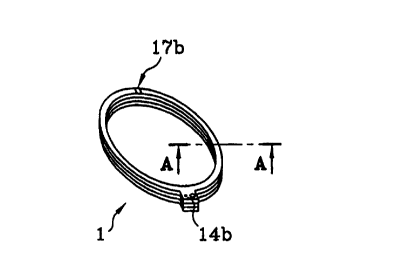
Acaord~.ng to a first embodiment, the antenna has a
general ~.oop shape and has a rectangular cross aect~.on
A-A. Thin ex~oaa section helps to reinforce its
geo~rietr~.c sta,bil~,ty. PreferabJ.y the loop ig ciroular
ae in the example. ,
Tn accordance with the invention, the shielded
magnetic-~ielr~ antenna has at least one turn 3b of a
metall~.c element and meta~.lic tl~bular shielding 5b, 6b,
?b, 6h disposed around the said element,
io In the example. the antenna has a s~.ngle thin flat
copper element 3b, disposed at the centre of a tubular
structure with a rectangular cross 'ection 5b, 6b. 7b,
8b . The el,emer~t 3b is sandwiched between two rings 9b,
~.2b t~a,de of insulating material and with a rectangular
is crow suction ~,Ob, 9b, preferably with the same
thicacnesa . I~ th~.s case the insulating material is
epoxy glass.
Ors each side of the element 3b, between the two
rzr~gs 5b, L2b, another inaulant such as air can be
2a found. or an adhesive connecting the two rings.
According to one variant, one of the two rings lZb
conpists of two rings 4b arid 10b connected together
(Fig 4), for example by gluing.
As for the tubular shielding, this consists of a
zs this, meta~.lic fi~.m, for example a 35 ~m copper film.
~n Figure 1, it can be peen that the shielda~ng
ring is open. It has a break 17b forming an a~.r gap
necessary to the oorrect functioning of the antenna in
accoxda~ae with a known teaching, the said air gap
3o berg disposed opposite the connection points 14b of
the antenna so that the eh~.elding arms have strictly
the same length.
Tn F~.gure~ ~ az~d 4 , it can be seen that the
antenna has at least two annular insulatix~.g supports : a
ss first top support 4b having the turn 3b on one of its
parallel daces, a portion 6b of th~ shielding being on,
CA 02270197 1999-04-23
7
the other ~ace, aid a eeaond bottom support 9b having
solely a portion 5b of the sh~.eZding.
Or~ce the two annu~.ar supports have been assembled,
fox example by gluing, their edge 11 receives a
meta~,l~.eation 7b, 8b which connects the portions 6b and
9b of each p~.de of the element. The metall~.eation can
be ef~eeted by any thin film depoeitior~ method, for
example by sprayi~.g ox mechanical deposition.
These metall~.e elements and the supports are
io advantageously printed-circuit elements. Conseguently)
it wild. be understood that producing the shielding uses
the technique of printed-circuit manufacture.
~acording to ~ vaxa.ant, only the turn 3b is
prpduced initially, the n~eta111c film 5b to eb is being
i5 produced together thexeafter, for example by spraying.
Another preferred embodiment will now be described
with the help of Figures 2, 5, 6.
According to this embodiment, the antenna 1 has a
general continuous shape xn block form, which affords
2o very good geometric pt~b~.lity.
~t consists of several cards made of in~ulating
material, three in Figure 2 or preferably two in
Figuxea 5 and 6.
Tn the game way as before, it has a turn of a
as metalla.c element 3a and a msta~.lic tubular shielding
5~, 6~, 7a, ea disposed around the said element.
T#~e turn is identical to the turn in the previous
example. On the other hand, there are differences in
the support and the lateral walls of the shielding.
3o The aupports_ are continuous cards whilst the lateral
wallp ce~aist of a plurality of metallic vial 7a and ea
connecting the two zings 5a and 6a.
These vine or aros5 members axe distributed on
each a~.c~e of the turn 3a along the latter (figure 9) .
35 Preferab~.y, these vies are spaced apart by as small a
distance as po~~i,b~.e so ~s to be effective at low
trequenc~.ea, zn the example, this distance is egual to
CA 02270197 1999-04-23
8
' 2.5 mm, t#~e diameter of the vial being 0.5 mm; this
distara,ce gives the antenna a good effio3ancylstrength
xat~.o in this example, which relates to the re$ding of
co~tac~leea chip cards.
s TYae vial pass through the cards 9a, x2a and
eleatr:~aally connect the ~.ateral edges of the metal7.ic
ring' of the ah~.eJ.ding. ,
A5 before, the card ~.2a carrying the turn can be
produced from two distinct cards 4a, 10a (Figure 6)
so corulected by gluing eubpequently or from a single card
12a, Whilst the other card 9a caxries solely a bottom
portion o~ the screening 5a.
As before, it can be seen in Figuxe 6, according
to a preferred embodiment, that the turn 3a and the
1s ririg 6a yre produced first of all on the same printed
circuit card 12a. wk~il,et the other ring ie also
produced in a pr~,r~ted circuit on another card.
These cards 9a and 12a are then apBembled, for
example by gluing,
20 lri a last operation, or~.fices are pierced a7.1
alor~g the lateral edges of the metallic rings in which
vise 7a, ea axe ~xoduced, like the ones normally used
in the production of pz~~,nted circuits . These vies ~ can
be xe~~.aQed by any ~Cinc~ of elongate metallic element
25 providing the same electrical connection function, for
example hollow or solid rivets.
Advantageously, the plurality of vices constitute a
per~o~ated wall o~ the screening in the same Way ae
braid of a coax~.al cable; it the~efoxe fulfils a
3o similar function.
Through the rigidity and geometric stability of
the printed circuit cards) a paxticu7.arly stab7.e and
reprod>~cible antenna is obtained.
Advantageously, the location 14a of the connection
ss and the location of the tuning c~,xcuit 13a are effected
on the same support as that of the antenxia.
CA 02270197 1999-04-23
Figure 7 i~.~.uetrates the metallisa~tions produced
on t~,~ee printed circuit cards 10a, 4a and 9a. At
least three metallieations are necessary: one
metallieation fox the top ring of the shielding 6a and
s for complettientaxy circu~.t elements 1.3a such as the
location of a tuning circuit Z4a and of a connector
x5a, another rnetallia~ation 3a for the turn, and a last
ore for the ring 8a and the above complementary cireua,t
elemerite 13a.
~o thus it is possible to create the antenraa and its
co~plementax~y electrical circuit elements in three
printing apera.tion~s. It suffices thereafter to
ae~semhle th-e thxee cards produced separately, to place
the visa on the card in an automated fashion, and then
to Goruzeot it and the components of the tuning Circuit
includ~,ng at least one variable capeaitor with very
f~.ne adjustment .
The card can have orifices ~.6a enabling metall~.e
inserts such as spacers to be introduced subsequently.
20 ~y vixtue of the use of a widespread manufacturing
method, it is poa~ible to produce such as antenna
eapily and rapidly on an industrial scale. Tn
ad,dit~.on, it ~.e also easy to change Format according to
the envisaged applications.
zs F~,gure A illustrates the three printed-circuit
cards 4a, 9a, 20a obtained here without the location o~
the tuning cixcuit. On the other hand, they have
respectively n ring 5a with a location 14a For
rece~.v~.ng a connector, a turn 3a and a ring 6a with
3o anothex location x4a.
Ire Figure 9, it can be seen that the vial 7a, 8a
era distributed a~.ong edges o~ the ring and that the
latter has an air gap i7a, disposed d~.ametrically
opposite t#~e eonneoting points 1,4a. '
35 In Figure 10, a magnetic-field antenna device 30
znoludea a printed-circuif antenna 2. Zn the example,
it ie a cane of the antenna accordir~g to the invention.
CA 02270197 1999-04-23
In this figure the antenna i~ equipped w~.th its tuning
circuit 23 and a connector 24.
The device 30 also has shie7.dir~g by means of a
matexia~, able to charW el electromagnetic waves, such as
s fox example a ferrite d ate 18 consisting of a set o~
flat fe~ri,te bare 19 disposed against each other and a
eereer~ against electromagnetic waves such as a steel
plate 20.
The assembly co~pisting of ferrite az~d screen is
~.o d~.spQSed succeesive~.y below the antenna 2 in Figure 10;
they must be interposed between the antenna sad the
metal~.ia surroundings. Such an arrangement isolates
the antenna from a metallic environment which could
disturb it.
~s According to the invent~.on, the ferrite assembly
18 ~,d isolated from the antsana 2 of the invention by
mee~ne of a leaf 21 of non-magnetic compressible
mate~~.al able to damp the mechanical vibrations or
impact. The same Material, in the form of a leaf or
Zo layer 22, is disposed. between the screen 20 and the
ferrite assembly. ~'h~ material can be compact such as
rubber or Neoprene-based foam.
Tn the example, Neoprene foam leaves have been
used, advantageously having adhesive faces so as to
zs facilitate mounting.
Thus it ie pospible to assemble different
breakable elements such as ferrite or ceram~.c with a
~r~.r~ted circu~.t element such as the antenna 2 of the
~.nve~t i on .
~'he anteru~,a device 30 can also have remote
adjuptment means 25 for Mode precisely controlling the
dietam.ces between the different layers formed by the
printed-circuit a~tenaa, the ferrite and the screen.
They can also have clamping means 26, 2~ for
as cor~tro7,ling the camping and the clamping together of
the ~,ayers .
CA 02270197 1999-04-23
m
In tire example, the antenna device 30 has spacer
pads 2S made from a denser material than the foam, for
example ten times denser and therefore ten times less
compressible under the same pressure, th~.e being
disposed laterally between the .steel gereeri 2o and th~
printed circuit 2 eo sa to keep a substantially '
constant diptaxice between them. The pads 25 can have
or~.~icea to enable the clamping means mentioned below
to pass:
The antenna device preferably has assembly and
cl~c~pa,ng means cor~e3sting in the example of four screws
26 ~.nd corre~~onding nuts 27 disposed at the four
carnar~ of tk~e s~ntenna 2) the nuts being integrally
fixed to the screen.
is As a varia~rt, aoakets 27 can be used which have
the function of nut and spacer, Thus, in tightening
the (screws completely there is always the game
separation and tY~s same compression of the leaves . The
az~tezma 2 can also have annular metallic inserts 28
2o which serve both as a waAher from the screws 26 and
whie~x hare a function of spacer for the printed-circuit
card.
Where applicable, the antenna can have a sole
plate 29 made of non-mag~etie flexible maternal such as
25 rubbed on which tl~e complete antenna can bear whilst
being isolated from the vibrations of the receiving
support.
Hy virtue of these aharacter~,stica, the antenna is
geometrically stable, since it ie not d~.aturbed by
so impacts o~ vibrations. In addition, the breakable
eletnenta being protected, it ofifers excellent
~echax~a.ca~l strength.
Moreover, it is po~sib7,e to manufacture ~.t simply
by aaset~~~-ng, and tk~is in a reproducible fashion.
35 In this application, the adjustable capacitors of
the tuning circuit can also be chosen with a very fine
adjustment.