Note: Descriptions are shown in the official language in which they were submitted.
CA 02270415 2005-06-29
FLEXIBLE WEARABLE COMPUTER SYSTEM
BACKGROUND OF THE INVENTION
1. Field of the Invention
The invention relates to personal computer systems, for example those
designed to be worn by a human user, and more particularly, to features of
such
systems that optimize comfort, miniaturization, processing speed, durability,
reliability and/or ease of manufacture.
2. Description of Related Art
Wearable computing devices of many different types are being used in a host
of commercial, industrial and consumer environments. Many such computers are
brick-like, however, concentrating a great deal of weight in a bulky,
cumbersome box
that must be strapped onto the body.
The best wearable computers are lightweight and flexible, demonstrating
1
CA 02270415 2005-06-29
superior ergonomics and allowing use during all normal activities. According
to
one example, flexible circuitry or equivalent flexible transmission devices
join
physically independent computer modules, allowing comfortable distribution of
the
computer about the body to accommodate a wide variety of body morphologies.
Standard-interconnect input/output devices allow easy user upgrades and
modular
replacements. Spread-spectrum ivireless Local Area Networks allow interaction
with other users and/or with a host computer system. Flexible wearable
computing
devices are comfortable, easy-to-use, convenient and powerful alternatives to
the
brick-like machines that until recently have been the only choice in the
marketplace.
Commonly assigned U.S. Patents Nos. 5,285,398, 5,491,651 and 5,581,492 to
Janik, and commonly assigned U.S. Patents Nos. 5,555,490 and 5,572,401 to
Carroll,
disclose a number of extremely
advantageous designs that are expected to dominate over previous, box-like
tivearable computers.
Recently, multi-chip module, thin-film circuit, and knmvn-good-die
technologies have allowed considerable miniaturization and standardization in
personal computers. U.S. Patent No. 5,422,514 to Griswold, for example,
discloses a number of advantageous packaging
structures and techniques. Griswold discloses a multi-chip module packaging
structure having a thin-film decal interconnect circuit fabricated on a thin
wafer of
2
CA 02270415 2005-06-29
aluminum or other material. MicroModule Systems, Inc. has developed and
produced a number of different multi-chip module and associated packaging
products.
Combining
known-good-die and die-on-board technologies has yielded packaging structures
with significant reliability and standardization advantages.
Given the many opportunities that have arisen with the introduction of
these technologies, it would be very advantageous to develop and specifically
adapt
these technologies in wearable-computing environments. Additionally, it would
be
very advantageous to develop connector devices, packaging arrangements, and
module-replacement technologies that can withstand the rigorous wearable-
computing environment.
SUMMARY OF THE INVENTION
To overcome the problems associated with prior devices and to achieve
various advantages, a number of computing systems and modules are described.
In one embodiment, a computing-device embodiment of the present
invention comprises an upper casing, at least one integrated chip module
electrically mounted on an interior side of the upper casing, a lower casing
selectively engageable with the upper casing, and flexible circuity extending
through
the upper casing and the lower casing, and being electrically connected to the
at least
3
CA 02270415 2005-06-29
one chip module within the lower and upper casing.
According to different embodiments of the invention, a unit casing is provided
with specialized attachment and/or connection mechanisms for providing secure
physical and/or electrical connections to the chip modules and associated
circuitry.
Further, the casing can act as a heat sink to actively aid in appropriate
management of
thermal radiation.
According to other embodiments, two circuitry-supporting substrates are
provided back-to-back to form an interior of a computing module, and an
exterior
case is disposed around the internal substrates. Standoffs and/or protective
encapsulant or gel are used to secure and protect the substrates within the
case.
In accordance with a further embodiment, a computing device comprises:
an upper casing;
at least one integrated chip module electrically mounted on an interior side
of
the upper casing;
a lower casing selectively engageable with the upper casing;
flexible circuitry extending through the computer device beyond the upper
casing and the lower casing, and being electrically connected to the at least
one chip
module and;
at least one electrical connector interposed between the integrated chip
module
and flexible circuitry.
In accordance with a further embodiment, a computing device unit comprises
an upper casing; a printed wire board including at least one integrated chip
module
electrically mounted thereon; a lower casing removably selectively engageable
with
the upper casing; a first protection frame interposed between and extending
about a
periphery of the upper casing and the printed wire board, and a second
protection
frame interposed between and extending about a periphery of the lower casing
and the
printed wire board; a portion of a flexible circuitry ribbon extending through
the unit
between the second protection frame and the lower casing; and at least one
electrical
connector interposed between and electrically connecting the portion of
flexible
circuitry and the chip of printed wire board; wherein selective engagement of
the
upper casing to the lower casing
4
CA 02270415 2007-11-30
secures the printed wire board, first and second protection frames, electrical
connector, and the portion of flexible circuitry within the upper and lower
casing and
secures electrical connection between the flexible circuitry and the at least
one chip.
In accordance with a further embodiment, a system of computing device units
interconnected to form a computer system comprises: a plurality of modules
wherein
each module further comprises: an upper casing; at least one integrated chip
module
electrically mounted on an interior of the upper casing; a lower casing
selectively
engageable with the upper casing; and a flexible circuitry ribbon extending
through
the upper casing and the lower casing, and being electrically connected to the
at least
one area grid array.
In accordance with a further embodiment, a system of computing device units
interconnected to form a computer system, the system comprises: a plurality of
modules wherein each module further comprises: an upper casing; at least one
integrated chip module electrically mounted on an interior of the upper
casing; a
lower casing selectively engageable with the upper casing; and a flexible
circuitry
ribbon extending through the upper casing and the lower casing, and being
electrically
connected to at least one area grid array.
In accordance with a further embodiment, a computing device unit comprises:
an upper casing;
at least one integrated chip module electrically mounted on an interior side
of
the upper casing;
a lower casing selectively engageable with the upper casing;
a flexible circuitry ribbon extending through the unit between the upper
casing
and the lower casing, and being electrically connected to the at least one
chip module
within the lower and upper casing;
wherein the chip is a ball grid array chip; and wherein an electrical
connector
is interposed between, and electrically connects, the ball grid array chip and
the
flexible circuitry within the upper and lower casing.
In accordance with a further embodiment, a flexible computing device
comprises a flexible computing module including a single computing circuit
disposed
on a single flexible sheet of flexible circuitry and including a first portion
foldable
over a second portion of the sheet, wherein the circuit extends contiguously
between
the first portion and the second portion free of a connector therebetween;
further
wherein the first portion is adapted for receiving a first modular connection
device
4a
CA 02270415 2007-11-30
and the second portion is adapted for receiving a second modular connection
device,
the first and second modular connection devices being readily receivable in
and
removable from the first and second portions.
In accordance with a further embodiment, a computing device comprises: an
upper casing;
at least one integrated chip module releasably electrically mounted on an
interior side of the upper casing;
a lower casing selectively engageable with the upper casing;
flexible circuitry extending through the computer device beyond the upper
casing and the lower casing, and being electrically connected to the at least
one chip
module, and
at least one electrical connector interposed between the integrated chip
module
and flexible circuitry.
In accordance with a further embodiment, a computing device comprises: an
upper casing;
at least one integrated chip module electrically mounted on an interior side
of
the upper casing;
a lower casing selectively engageable with the upper casing;
flexible circuitry extending through the computer device beyond the upper
casing and the lower casing, and being electrically connected to the at least
one chip
module, and
at least one electrical connector interposed between the integrated chip
module
and flexible circuitry;
wherein the at least one integrated chip module is releasably connectable to
one or the other of an external peripheral computing device and another
modules.
Embodiments of the invention are well-suited to BGA and other packing
technologies and provide fast, small, durable, and cost-effective design
configurations
that represent significant improvements over prior-art wearable computers.
Other
features of the Invention are described below.
4b
CA 02270415 2008-01-15
BRIEF DESCRIPTION OF THE DRAWINGS
Embodiments of the invention will be described with reference to the figures,
in which like reference numerals denote like elements and in which:
Figure 1 is a schematic illustration of a flexible wearable computer system
incorporating a computer module according to embodiments of the present
invention;
4c
CA 02270415 1999-04-30
Attorney Docket No. 1229.10WO01
Figures 2-3 are side views of computer module case portions with connector
elements, according to embodiments of the invention;
Figure 4 is a perspective view showing a connector portion according to an
embodiment of the invention;
Figures 5-6 are partial cross-sectional views of computing modules according
to embodiments of the invention;
Figures 7-8 are schematic and perspective views, respectively, of a battery
and/or computing-module system according to an embodiment of the invention;
Figure 9 is a side view of a hinged computing module according to an
embodiment of the invention;
Figure 10 is an exploded perspective view showing another embodiment of
the present invention, for producing a secure connection to flexible
circuitry;
Figure 10A is a plan view of a module and frame arrangement according to
an embodiment of the invention;
Figure 11 is a cross-sectional view of the embodiment of Figure 10;
Figure 12 is an enlarged view of the embodiment of Figure 11;
Figure 13 is an alternative embodiment of the embodiment of Figures 10-11;
Figure 14 is an exploded perspective vieiv of the embodiment of Figure 13;
Figure 15 is a cross-sectional view similar to Figure 13;
Figure 16 is an enlarged viecv of a portion of Figure 15;
Figure 17 is a perspective view of a slotted-module embodiment according to
CA 02270415 1999-04-30
Attorney Docket No. 1229.10WO01
the invention; and
Figure 18 is a plan view of a dimpled-surface arrangement according to an
embodiment of the invention.
DETAILED DESCRIPTION OF PREFERRED EMBODIMENTS
Embodiments of the invention have wide application to a number of
different computing technologies and environments. As discussed above,
flexible
wearable computers are gaining rapid acceptance in the marketplace in
different
computing environments, including rriilitary, maintenance, law enforcement,
medical and other environments. Further, miniaturization and ease of
manufacture are important in virtually all computing environments, not just
those
well-suited for wearable computers. Thus, although particular embodiments of
the
invention will be discussed with respect to wearable computers and in
particular
flexible wearable computers, the invention is not necessarily limited to those
embodiments.
Accordingly, Figure 1 illustrates a flexible, wearable computer system 10
including an integrated set 14 of computing modules 12 (e.g. body LAN, audio &
video, flash memory, etc.). Modules 12 function in association with input and
output devices 16 (e.g. keyboard, bar code reader, mouse, microphone, etc.),
display
devices 18 (e.g. VGA monitors, liquid image displavs), and battery 20 via
ivired
and/or wireless connections.
6
CA 02270415 1999-04-30
Attorney Docket No. 1229.10WO01
Figures 2-3 illustrate examples of modules 12 and an example of the manner
of connection of modules to another module or an external peripheral device.
Computing-module case 300 includes broken-away portions to show certain
internal
features. Module portions 300 include connection port(s) 305 with tabs 310,
e.g.
bordered by corresponding notches 320, for receiving connectors 330 (e.g.
ribbon
cable connectors, PC-card connectors, or other type of connector) useable with
a
portable or other computing device. Illustrated connector 330 (Figure 2)
extends
from cable 306 of a peripheral device or other computing device (not shown).
Recessed connection port 305 with notches 320 (Figure 2) enables computing
module 300 to compensate for the tendency of cable 306 and/or connector 330 to
pull
sideways or at a sharp angle relative to module 300. Recessed and notched port
305
is important, because a significant factor weighing against the durability of
any
wearable computer device or other portable electronic device is connector
strain.
Embodiments of the invention enhance a robust connection, by including e.g. a
recessed connection port to prevent cable connector 330 from forming a sharp
angle
relative to module 300, notches 320 and flexible tab 310, which permit flexing
of
connection port 305 with movement of connector 300.
Tabs 310 are constructed to flex with respect to the remainder of module case
portion 300, for example by etching away the aluminum or other base material
to
leave a thin, flexible remainder. Traces and/or other signal-conducting
elements
335, optionally including S-curved portions 337, are loosely mounted on but
not
7
CA 02270415 1999-04-30
Attorney Docket No. 1229.10WO01
bonded to tab 310 of case portion 300, according to one embodiment. Traces 335
connect to circuit elements 340, which can include die-on-board devices, multi-
chip
modules, discrete elements, etc. supported on case portion 300 at its central
portion
over etched and filled traces of suitable connection circuitry.
By leaving traces 335 loose on tab 310, tab 310 can "give" or bend slightly,
if e.g.
connector 330 is attached to it with undue or excessive force, without
breaking the
traces or subjecting them to unacceptable stress. S-curves 337 or other slack
can be
incorporated into traces 335 to better accommodate this bending movement. This
represents a significant advantage over prior art devices, which are subject
to
significant trace damage if a connector is "jammed" into place.
Alternatively, tabs 310 can be made rigid with the remainder of case portion
300, and the associated traces and/or other signal-conducting elements bonded
directly to tab 310. Directly bonding the circuitry ensures the substantially
absolute
planarity that is often desirable during etching and depositing operations,
for
example.
As shown in Figure 3, tabs 310 can be associated with PC-card or other
connector(s) 350, docking connector(s) 360 for docking to e.g. a desktop
computer,
and/or battery and poiver connector(s) 370. Docking station/connector 360 can
provide input/output for CRT's, LCD's, sound, keyboard, mouse, etc., or can
provide connection to a separate computer, as will be described. Further,
docking
connector 360, as well as the other connectors, are optionally recessed
ivithin the
8
CA 02270415 1999-04-30
Attorney Docket No. 1229.10WO01
remainder of substrate 300 for protection. Of course, a wide variety of
connectors
can be used, and individual connectors can be designed to receive multiple
connecting devices, for example both PC cards and a battery.
In particular, module 300 in Figure 3 includes a single slot 372 between two
connection ports 373A, 373B to permit flexing in a manner similar to the tab
configuration in Figure 2. However, in Figure 3, the unrestricted edges 374 of
module 300 effectively act as another slot permitting flexing of each
connection port
373A, 373B. Moreover, tab 360 preferably is recessed even further than tab 310
( in
Figure 2) and also includes notches on its sides. Connector 370 provides a
similar
protective arrangement for a poiver supply connection, only having a deeper
recess
and slits 376 instead of notches 320 to achieve the desired flexibility. In an
alternative arrangement, the Figure 3 embodiment also includes tabs 310
covered by
a non-conductive material 345.
Instead of using a separate desktop computer to -,,vhich a user's wearable
computer is docked upon his or her arrival, the user's work environment can
include merely a set of peripherals. Upon arrival at the ,,vork environment,
the
user can easily connect the wearable computer to various peripheral connectors
there, for example display, keyboard, mouse and/or power connectors.
Eliminating
the desktop computer and using the wearable computer in its place is extremely
advantageous, reducing hardware costs and freeing up desk space, for example.
According to a one embodiment, the wearable computer itself is mountable
directly
9
CA 02270415 1999-04-30
Attorney Docket No. 1229.10WO01
onto one of the work environment devices, for example by VELCRO to a display
device.
According to another embodiment, a connector is recessed within case
portion 300, the aluminum or other material out of which case 300 is formed
being
disposed over the connector to protect it. The strength of the aluminum
supports
the relatively weaker connector portion or exposed element associated with it,
for
example an emerging wire. If a thick enough slab of material is used as the
case, the
connector can be fully shrouded for enhanced protection. The shroud can simply
be
stamped onto the same metallic material onto which the device is being built,
Figure 4 illustrates an alternative connector design, in which case portion
300
is connected at ribbon cable connector 345 to at least one ribbon cable 346.
Cable 346
is connected in turn to PC-card connector 347 or other type connector, for
example a
connector of an adjacent computing module.
Figures 5-6 are partial cross-sectional views of internal computing module
features according to embodiments of the invention. Module 400 comprises two
external substrates 430, formed of e.g. aluminum. Substrates 430 have
associated
circuitry 433 fabricated/bonded thereon. A plurality of standoffs 440 separate
substrates 430, to protect circuitry 433 and any other enclosed componentry
from
side-to-side squeeze pressure on module 400. Standoffs 440 are preferably
formed of
metal, rubber, TEFLON, or other materials, and can be arrayed in a desired
pattern.
According to one embodiment, standoffs 440 also act as connectors (e.g.
elastomeric
CA 02270415 1999-04-30
Attorney Docket No. 1229.10WO01
connectors) between circuitry 433 of upper and lower substrates 430, either by
being
formed of a conductive material or by having internal traces, for example.
The Figure 5 embodiment also includes an optional bounce-resistant or other
protective coating 450, disposed directly on substrates 430, to further
protect circuitry
433. Of course, coating 450 can be disposed on the modules of the other
embodiments disclosed herein as well.
Moreover, in Figure 5, the substrate 430 can form the casing of the computing
module (e.g. a module like module 12) and has electrically connected thereon
circuitry 433 so that the substrate casing ivall 430 effectively functions as
a printed
,vire board. This arrangement of the casing forming the chip board is
particularly
advantageous with continued miniaturization, e.g. wherein the circuitry
ultimately
will comprise an entire computer itself. Accordingly, circuitry 433 can
comprise
several multi-chip or other packaging modules forming part or all of a
computer
housed within substrate casing 430.
According to the Figure 6 embodiment, module 500 includes two internal
substrates 530 that are formed of e.g. aluminum and that support circuitry
533.
Substrates 530 are disposed back-to-back within external case 515, with
circuitry 533
facing outwardly relative to the substrates. Case 515 can be formed of a rigid
protective material, a flexible lithium-ion battery as discussed above, or
other
suitable materials/devices.
Aligned apertures 535 extend through back-to-back substrates 530 to receive
11
CA 02270415 1999-04-30
Attorney Docket No. 1229.10WO01
standoffs 540. Standoffs 540, composed of metal, rubber, TEFLON, or other
materials, can be rigidly attached to external case 515 so as to center or
otherwise
hold substrates 530 in position within module 500. Alternatively, standoffs
540 can
"float" with respect to case 515 and merely fix the relative positions of
substrates 530.
In either case, standoffs 540 protect circuitry 533 and any other enclosed
componentry from side-to-side squeeze pressure on module 500, and can be
formed/arrayed as described ivith respect to the previous embodiment. Also as
with
the previous embodiment, standoffs 540 optionally act as connectors (e.g.
elastomeric connectors) between circuitry 533 of upper and lower substrates
530, or
between circuitry 533 and case 515.
Optionally disposed within the space between circuitry 533 and case 515 is
protective material 545. Material 545 can include an elastomer material, foam,
encapsulant, or other shock-absorbing or dampening material, to further
protect
circuitry 533 from outside forces.
Thus, as shown in Figures 5 and/or 6, the surface where the ASIC is
mounted, e.g. surface 515, becomes the case of the processing device. It is a
combination mounting area for the ASIC, as in the board of a BGA, whether it
is
aluminum or some other surface that the ASIC is mounted on. And it becomes the
case of the processing device itself. Multi-chip modules with multiple ASIC's
can be
are mounted on a single backplate that is mounted as a single chip device,
according
to embodiments of the invention. As these are laid out on e.g. a single board
12
CA 02270415 1999-04-30
Attorney Docket No. 1229.10WO01
backplane, and as multi-chip modules get large enough to be an entire
computer,
and as they are face-to-face in order to allow the backside of any device
mounting
means, like an ASIC against aluminum, to become the case for the computer,
compactness is greatly increased. At the same time, however, the surfaces are
prevented from being smashed together by the separation/elastomeric means,
which also form a conductor between the two surfaces.
Figures 7-8 are top and perspective views of a flexible, wearable-computing
and/or battery system 600 having multiple battery sections or computing
modules
arranged in layers and usable with wearable computers according to the
invention.
A central connector 620 electrically interconnects the multiple battery and/or
computing-module layers 610. This configuration can be used for either battery
design or processing design, and can include combinations of both batteries
and
modules in a layered arrangement. In other words, a single module layer can
include only one of a battery or a computing module, or a single module layer
can
include a battery on one side of the layer and a computing module on the other
side
of the same layer. This flexible, multilayer design permits central connector
620 to
be conveniently disposed in the middle of the back of a human wearer, for
example,
to permit the multiple layers to extend and gently curve about the wearer's
body in a
non-binding fashion not obtainable in ordinary belt, linear flexible-wearable
or
other computer-module arrangements.
In other ivords, system 600 includes a plurality of flexible battery or
computer
13
CA 02270415 1999-04-30
Attorney Docket No. 1229.10WO01
segments 610 connected to a central member 620. This layered design is
particularly
advantageous in wearable-computing environments, in which body morphology
should be well-accommodated to provide the greatest degree of physical
comfort.
Each segment 610, which advantageously can comprise an individual battery cell
or
individual computing module, can move independently, minimizing compression,
stretch or other stress upon the overall system 600 as it is required to bend.
In a battery embodiment, connector 620 is connected by e.g. wire 625 to power
supply 630. Power supply 630 includes a power supply transformer and logic,
providing a direct and clean interconnect to the remainder of the computing
device
,,,vith minimal adverse emissions/noise. The power supply preferably is sold
with
member 620 and cells 610 to form an integrated battery system unit.
Battery system 600 can be selected to supply a desired voltage level for a
particular computing application, e.g. 12 volts, 5 volts, 3 volts, or mere
back-light
voltage. Battery system 600 is connected to the computing module(s) of the
wearable
computing system by any desired means. Of course, as mentioned above, the same
configuration can be used to implement a layered system of computing modules
with or without a system of layered batteries.
Computing-module embodiment 700 of Figure 9 includes tivo substantially
identical halves 710, each including PC-card or other connectors 720 for
receiving
respective PC cards or other e.g. modular connection devices 730. Individual
halves
710 are connected by hinge portion 740, which preferably is formed by etching
away
14
CA 02270415 1999-04-30
Attorney Docket No. 1229.10WO01
the base material (e.g. aluminum) to a minimal thickness, for example, or by
an
alternative process. The PC cards or other connection devices are individually
routed within module 700, but interconnects between halves 710 are run in
connection with hinge 740.
Figure 9 illustrates a single computing sheet having a small enough thickness
for sufficient flexibility to bend around or otherwise accommodate the body.
The
two portions connect at one edge, fold over and function as one folded piece.
The
singularity of the module permits curving about the body yet does not bind
against
the wearer of the module because the two portions act as a single unit due to
their
connection along one edge. Electrical connections can be formed between
portions
710 along entire edge 740 in the fold, allowing circuits to be placed on in
essence four
sides when it is folded over. A "butterfly" configuration as in Figures 7-8 is
also
contemplated. Thus, a narrow belt configuration can be produced, having enough
space for connection wires. Module 700 can be formed as a single circuit or
motherboard without a separate interconnection at fold 740. Thus, an entire
motherboard can be built as one sheet and folded it in half to be positioned
on the
body in a comfortable fashion and/or in a relatively compact space.
As an alternative to the Figure 9 embodiment, a notch or connector can
interface -vvith the far end of the PC-card or other connector slot, so that a
flexible
interconnection is formed that can be folded over such that one end can be
tucked
into the other. In a battery-as-case embodiment, interconnects join the
battery/case
CA 02270415 1999-04-30
Attorney Docket No. 1229.10WO01
to the circuitry on the substrate.
A flexible wearable computer system according to embodiments of the
invention is readily modularizable, allowing a variety of possible
configurations, as
shown in Figure 1. Assuming sufficient miniaturization of the various
connectors,
for example, the wearable computing system can be radially constructed. A
plurality
of radially spaced connectors can be used, for example eight, and various
input/output devices interchangeably affixed to any one of the connectors. The
main portion of the computing device can then be worn around the left armpit
in a
shoulder holster, ivith one or more PC-card connectors and PC cards extending
downwardly along the wearer's side. A battery runs from the most appropriately
placed radial to come around to the right armpit for supporting the batteries.
This
dual shoulder holster arrangement provides an ample power supply and
advantageously distributes and supports the weight of the system around the
wearer's body.
A wide variety of thermal management arrangements are possible according
to embodiments of the invention. For example, heat-distributive material can
be
disposed within one or more of the disclosed computing modules in various
shapes
or patterns, to route heat most effectively. Mounted in an "X" pattern, for
example,
the heat distributive material distributes heat from a central, thermally
active
portion out-vvardly to cooler distal portions. Heat-distributive material can
also be
disposed outside the case in various patterns, e.g. butterfly or "X" patterns,
within an
16
CA 02270415 1999-04-30
Attorney Docket No. 1229.10WO01
outer flexible shell. As the user leans back against a supporting surface,
e.g. the back
of a chair, the heat-distributive material redistributes within the shell to
more
effectively mix together and thus transfer heat from the module. Thus, thermal
energy transfer is enhanced and facilitated.
According to preferred embodiments, dimensions of a wearable computing
module using the technologies described above are significantly reduced.
Modules
according to the invention can be as small as or smaller than 2-1/2 by 2 by
3/8
inches, readily accommodating e.g. 2-1/8 inch PC-card or other connector
widths.
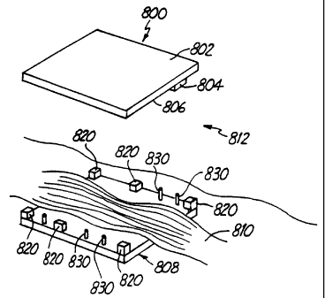
Figure 10 illustrates computing device unit 800 comprising upper casing 802,
at least one integrated chip module 804 electrically mounted on interior side
806 of
upper casing 802, lower casing 808 selectively engageable with upper casing
802, and
flexible circuitry ribbon 810 extending through the upper casing 802 and the
lower
casing 808. Flexible circuitry ribbon 810 is electrically connected to chip
804 within a
sealed frame 812 defined by upper and lo-vver casings 802 and 808.
Figure 11 illustrates computing module 800 in an assembled view. As
shown, due to compression (further described below) between upper casing 802
and
lower casing 808, chip module(s) 804 is/are in electrical connection with
flexible
circuitry ribbon 810 without any intermediate connector to provide a thin,
robust
computing module ideal for a flexible wearable computer system.
Integrated chip module 804 can be a MMS-type processor module, or of other
types including MCM, MCP, BGA, and microBGA. The computing module
17
CA 02270415 1999-04-30
Attorney Docket No. 1229.10WO01
configuration of Figure 10 can implemented as any of modules 12 (e.g. body
LAN,
audio, video, flash memory, global positioning, CMOS digital camera, body
sensors,
radar sensors) shown in Figure 1, for example.
Module 800 further includes protection frame 820 including an
electromagnetic interference capability and arrangement to effect a seal for
frame
812. A sealing cap is configured and arranged in one or several portions 820
to
protect electrical circuitry and align the electrical components as well as
the upper
and lower casings 802 and 808. The protection frame can also function
simultaneously as a elastomeric connecfor, and/or to be the electrical contact
point
for the module 800.
Frame 812 is provided with sufficient rigidity by having rivets 830, blind
rivets, or other suitable connectors 830 in cooperation with protection frame
elements 820 as necessary. A matching frame or frames with properly placed
holes
is lined up with the first frame, and the two (or more) are pressed together,
simultaneously or sequentially, to form an assembly that is preferably a one-
time
press-together fitting.
As shown in Figure 12, elastomeric connector 840 (see further examples in
Figures 13 and 14) can be placed between flexible circuitry 810 and chip
module 804
and be compressed appropriately, ensuring consistency and adequacy of
electrical
contact inside the frame/module. To facilitate alignment and electrical
connection,
elastomeric connector 840 can be of many different shapes. For example, the
18
CA 02270415 1999-04-30
Attorney Docket No. 1229.10WO01
elastomeric connector can be rectangular, elongate, and/or form a border about
the
module (e.g. for a tape automated ball grid array). Moreover, the elastomeric
connector can form a portion of protection frame 820 to reduce the total
amount of
material for constructing module 800. With this and previously described
embodiments, an elastomeric or other connector can be used, and it can have a
number of wires or traces stuck into/through the connector and cut off at the
end.
At the end, then, precise alignment with e.g. the ball(s) of a BGA is not as
much of a
concern, as long as sufficient contact is made with a sufficient number of
wires in
the connector. Thus, solder-free connection of a BGA or other module with
flexible
circuitry or other signal-carrying component can be accomplished.
Protection frame 820 can be continuous (see Figure 14, to be described,) or
broken into portions (Figure 10), and can extend around or pass through a
portion of
the flex circuitry. In addition, protection frame 820 can act in substitute of
pins 830
and/or be formed in a combination of blocks that interlock for compression,
alignment, and protection of the circuitry to provide a seal and EMI
protection. In
addition, cvhen protection frame 820 is broken into portions, it can include
portions
that are formed as part of the chip module 804 to provide the balance of the
protection frame 820. As shown in Figure 10A, protection frame 820 can be
attached, molded or otherwise formed as a ball grid array (BGA) chip package
to
form a border around a BGA package module 804. This concept can be applied
throughout casing frame 812 to eliminate need for a separate protection frame.
19
CA 02270415 1999-04-30
Attorney Docket No. 1229.10WO01
Lower casing 802 acts with the upper casing 808 to ensure secure connection
between flex circuitry 810 and BGA package 804, e.g. keeping the balls from
slipping
and aligning the entire unit assembly 812 to ensure electrical contact in the
appropriate areas of flex circuit 810.
Figure 13 illustrates a stacked-configuration module 800 having a printed
wire board 850 suspended between lower casing 808 and upper casing 802 with
chip
modules 804 on each side of board 850. Protection frame 820 seals frame 812
and
separates the respective casings. In addition, an elastomeric connector 840
facilitates
connection of chip modules 804 cvith flex circuitry ribbon 810. Embodiments of
this
configuration are shown in an exploded view in Figure 14 and in Figures 15 and
16.
In the embodiment shown in Figure 17, chip module 804, e.g. a BGA module,
MCM or other module, e.g. as described above, is also removably insertable
into
position and electrical connection against upper casing 802 and/or protection
frame
820 and/or elastomeric connector 840. For example, upper casing 802 can be
removed, chip module 804 removed and another chip installed in its place. This
exchange can also be performed from a side of the unit through formed slot 870
which is adapted to receive a chip module inserted into the casing. Module 804
is
then electrically secured against the casing and electrical connector (e.g.
elastomeric
connector) to the flexible circuitry- by mechanical compression with an
exterior clip
875 about the casing, a ~vedge action or other means to make the contact. Snap-
fit,
screived-together, levered or other mechanical means to provide the
compression
CA 02270415 1999-04-30
Attorney Docket No. 1229.10WO01
are contemplated according to the invention.
In this mechanism, the casing and/or protection frame includes alignment
guides 878 to guide module 804 as it is slidably inserted into and through
edge 872 of
the casing unit. Once module 804 is guided within the protection frame, it
drops
into a reciprocating electrical connection pad. To secure the electrical
contacts, an
insertable wedge or other mechanism for applying exterior pressure to the
casing is
used (e.g a clip). To facilitate the placement and connection of the module to
the
upper casing 802, interior side 806 of the upper casing can include a dimpled
area 880
(Figure 18) for accommodating/reciprocating the ball arrays on a BGA module or
the
connection elements of another desired module.
In this configuration, to exchange a module, a technician opens the upper
casing, causing the module to pop up preferably with some mechanical
assistance.
This permits the module to be removed from the casing unit. Next, the
technician
slides a replacement module into the casing from the edge slot 870 wherein the
alignment guides 878 within the casing cause the module to slide downward to
the
reciprocating connection pad. The technician then selectively secures the
upper
casing to the lower casing to close the unit and thereby securely electrically
connect
the module between the upper casing and the flexible circuitry by compression
of
the upper and lower casing against the electrical components disposed
therebetween.
Of course, as mentioned above, this connection can be made without solder
21
CA 02270415 1999-04-30
Attorney Docket No. 1229.10WO01
due to the combination of automatic alignment and mechanical compression and
can be further facilitated through the use of flexible elastomeric connectors
placed at
the point of electrical connection between the module and flexible circuitry
or other
intermediate surface of electrical connection.
The Figure 17 embodiment can also include a pair of unit casing side slots
870B and is capable for selectively ejecting a single module 804 into and
through first
slot 870 of casing frame 812. Compression on the upper and lower casing 802,
808 is
partially relieved so that upon insertion of a replacement module 804 , the
existing
module is forced out of position of the unit casing and ejected from the
casing
through second slot 870B. The replacement module is guided into place and then
compression (via clamp, snap-fit or the like) is again applied between the
upper and
lower casing 802, 808 of the unit to securely electrically connect the
replacement
module in place relative to flexible circuitry 810.
This arrangement permits selective replacement of e.g. a BGA chip module
802 while avoiding or at least minimizing handling of it. Excessive handling
can
contaminate the electrical contacts and cause short circuits or other
damage/problems. According to embodiments of the invention, a user in the
field
can substitute different modules having different functions, as needed.
A chip 804 that is an MMS processor advantageously, can be on an aluminum
blank, or equivalent, as described above, preferably conductive of heat to the
outside.
Protection frame(s) 820 in e.g. Figure 14 are placed between the pressed-
22
CA 02270415 1999-04-30
Attorney Docket No. 1229.10WO01
together fittings to take up the space along the electronic parts to be
suspended in the
module on the boards. The frame(s) preferably are tolerant, allolving
compression
of the elastomeric connector(s), and seal the electronics from the outside
world.
They also preferably provide EMI continuity. More or less than the tcvo
illustrated
protection frames can be provided, depending on the number of board layers
provided.
Also in Figure 14, elastomeric connector(s) 840 preferably extend from the
flexible circuit, the flexible backplane, to the first of the boards.
Additional
connector(s) extend between additional boards, as needed. In the case where
the
MMS-type processor module 804 is used, as illustrated, the connector 840
preferably
reaches the circuitry 810 bonded to the board 850. Backplate lower casing 808
preferably is a protective and restraining backplate that the fasteners
connect to,
protecting the flex circuit layer 810 and providing a support for the
compressing of
the elastomeric connector(s) and bonding.
Locator means, preferably the holes into which assembly means 830 (e.g.
rivets, closure pins, compression pins, ratcheting inside-outside plastic- or
nylon-
type connectors with closely spaced and/or precisely spaced teeth on a post
inserted
going into an internally toothed shaft, etc.) are precisely placed, are
provided. They
can be bonded to one side and compressed on the other, according to one
embodiment. One of their primary functions is to properly locate the
illustrated
components with respect to each other, so that the electronics of the various
layers
23
CA 02270415 1999-04-30
Attorney Docket No. 1229.10WO01
match up with each other through the stack. A series of preferably evenly
spaced
locator pins or other fasteners are located on both sides of the elastomeric
connector(s) to prevent arching effect.
While the invention has been described with reference to specific
embodiments, the description is illustrative and is not to be construed as
limiting
the scope of the invention. For example, features of the various disclosed
embodiments can be mixed and matched to suit a particular application; e.g.
the
disclosed battery system can be used with any of the disclosed module
embodiments.
Additionally, the illustrated and described features can be used with not only
wearable but other types of computing devices. Wireless or wired, infrared,
optical,
and other communication schemes are contemplated. Instead of flexible
circuitry,
ribbon or otherwise, additional signal-relaying componentry can be used in all
embodiments of the invention. By "signal" is meant power signals, data
signals,
and other electrical, optical, IR, RF or other signals providing transmission
and/or
communication. Various other modifications and changes may occur to those
skilled in the art without departing from the spirit and scope of the
invention.
24