Note: Descriptions are shown in the official language in which they were submitted.
CA 02270816 1999-OS-03
1
Title of The Invention
ZERO VOLTAGE SWITCHING BUCK DERIVED CONVERTER
Technical Field of the Invention
io The present invention relates generally to isolated DC-DC converters and
more particularly to buck derived converters which feature zero voltage
switching
of the controlled power switches and zero current switching of the non-
controlled
switches.
is Background of the Invention
DC to DC converters are frequently used to convert DC voltage, provide
galvanic isolation of the output from the input, and to regulate the output.
DC to
DC converters are also frequently used as a portion of AC to DC power
supplies.
2o For example such power supplies are employed in Telecommunication or
Cellular
Power Systems to provide isolated 24Volt or 48Volt power to the system
batteries
and paralleled load. DC to DC converters are also frequently used to convert
and
isolate one DC voltage from another. For example, +24Volt cellular site power
is
converted to -48Volt for co-located telecommunications equipment by using
2s DC/DC converters.
Of the many topologies that can be used for DC-DC converters, those that
are buck derived are often preferred for medium (+24V, 48V) and low (5V, -3V)
voltage outputs. This is due to the non-pulsating output current and ease of
control
CA 02270816 1999-OS-03
2
as the output voltage is directly proportional to the duty cycle of the
switching
devices. A common buck derived converter is the forward converter discussed in
"The Forward Converter in Switched-Mode Power Supplies", Philips Application
Note #474, 4 July 1975. This converter features good component load factors
(see
s "Converter Component Load Factors, A Performance Limitation of Various
Topologies" Bmce Carsten, PCI'88 Munich, Germany), relative simplicity, ease
of control and non pulsing output current. Another buck derived converter is
the
half bridge exemplified in "Switched Mode Power Supplies -- Highlighting a SV
40A Inverter Design", Motorola Application Note #AN-737, 1974. This converter
is more complex with 2 primary power switches, and has the disadvantage of 2
output windings, in the power transformer. Other commonly used buck derived
converters are the full bridge PWM controlled and the phase shifted bridge
converters. The component load factor of the forward converter was improved
with the use of an active reset switch as disclosed in "High Power SMPS
Require
~s Intrinsic Reliability", Bruce Carsten, PCI'81 Proceedings pp. 118 to 133,
Munich,
Germany, Sept 1981.
One objective in designing a DC-DC converter is to achieve low switching
losses and low EMI. This can be achieved by adding capacitors across the
primary
2o power switches and by operating the circuit in such a way to bring the
voltage
across them to zero before turning them on. This approach was disclosed in
Jitaru
US Patent 5,126,931 in the active reset forward converter by adding a
saturable
reactor, or third controlled switch, in series with the output winding of the
transformer and reducing the magnetizing inductance of the transformer to
allow
2s the voltage of the main switch to ring down to zero before it is turned on.
CA 02270816 2003-03-14
.3
Another class of DG/DC converters use asymmetrically controlled half bridge or
full bridge switches, where either switch is on except during the switching
times
and the output is controlled by the relative duty cycle of the switches.
Examples of
such a converter are described in "Soft-Switched DC;/DC Converter with PWM
Control", Ramesh Origami et al, Proceedings of Intelec 93 Paris, France Sept
'93.
The first is similar to a flyback (bucklboost) converter. The second is
somewhat
similar to a buck derived converter but has a non-linear parabolic transfer
function
with maximum output at SO% duty cycle and would be difficult to control.
Another such converter topology is described in "DC/DC Converter for High
Input
1o Voltage, For Switching with Peak Voltage of Vir~/2, Capactive turn off
Snubbing
and Lero Voltage Turn on", I. Barbi et al, PESC '98 Fukuoka, Japan May '98,
and
is similar to a phase shifted full bridge converter. This converter topology
suffers
from substantial extra current in the transformer windings when both half
bridge
sides are switched to the same input voltage. This circuit will have a poor
1s transformer load factor except at SO% (full) duty cycle.
It is accordingly an object of the invention to provide a new and improved DC-
DC
converter most suitable far medium output voltages such as 24 Volts or 48
Volts
DC.
An additional object of the invention is to provide a DC-DC converter with an
isolated output which is proportional to the control duty cycle, and has a non-
pulsating output current. A further object of the invention is to provide zero
voltage switching of the controlled power switches (e.g. MOSFETS, namely metal
oxide silicone field effect transistors) and zero current switching of the
output non-
controlled switch (e.g. a diode) to maximize conversion efficiency and
minimize
EMI, without using an additional switch in
CA 02270816 2003-07-24
series with the output.. Another object of the invention is to provide a DC-DC
converter with high component load factor .for the switching devices and
especially the transformer to minimize size and cost.
s
Summary Of The invention
In one of its aspects the invention consists of a switch mode DC to DC
converter
comprising a half' bridge or full bridge arrangement of asymmetrically
controlled
to switches at the input stage, a primary DC' blocking capacitor in series
with the
primary winding, and an output stage having an output capacitor with one end
connected to a first er~d of :m output inductor and the output capacitor being
connected in parallel with the output terminals and further including a series
combination of a secondary I)C blocking capacitor and the secondary winding,
1s one end of the series combination being connected to a second end of the
output
inductor, and an output diode connected across the; series combination.
The primary half bridge stage nay be realized by two controlled switches in
series
with one another, the series combination being in parallel with the input
terminals.
2o Antiparallel diode means are associated with each switch and are poled to
allow
current to flow in a direction opposite to the normal direction of current
flow in
each switch. An inductor is in series with the primary winding and at least
one
primary DC blocking capacitors the series combination of the inductor, primary
winding and primary DC blocking capacitor being connected between one of the
2s input terminals and the common point of said two controlled switches.
The primary DC blocking capacitor may in fact be two capacitors such that each
capacitor is connected to one of the input te1-minals.
CA 02270816 2003-07-24
s
The primary stage may also be realized as a full bridge arrangement of
switches.
Two asymmetrically controlh;d switches are connected in series with one
another
and in parallel with the input terminals and with a further two asymmetrically
controlled switches which are also connected in series with one another.
t~ Antiparallel diode means are associated with each switch arid are poled to
allow
current to flow in a direction opposite to the normal direction of current
flow in
each switch. An inductor is in series with the primary winding and a primary
DC
blocking capacitor, the series combination of the inductor, primary winding
and
primary DC blocking capacitor being connected between the common point of the
to first two controlled switches on the one hand and the common point of the
further
two controlled switches on the other hand.
In another aspect, the invention comprises a clamp diode means and a clamping
capacitor connected in series across the output diode. The clamp diode is
puled to
is conduct opposite to the normal direction of current flow when the switch is
ON. A
controlled energy recovery switch is connected across the clamp diode means
and
is poled to conduct current in the opposite direction to the normal direction
of
current in the clamp diode means when the controlled switch is turned ON.
2o In another aspect, the invention comprises switch control means for
controlling the
operation of the controlled energy recovery switch such that it is closed at
substantially the same time as one of the controlled switches.
In another aspect, the invention comprises a discrete capacitor connected
across
2s each of the control switches.
In another aspect, the inductor means of the invention is a discrete inductor
in
series with either the primary winding or the secondary winding.
CA 02270816 2003-07-24
In another aspect of the invention, the inductor means is realized as the
leakage
inductance of the transformer.
In another aspect of the invention, a converter with a half bridge or full
bridge
:> primary stage includes an output stage including a secondary DC blocking
capacitor in series with the secondary winding, one end of the series
combination
being connected to a tap on an output inductor, and an output diode connected
across the combination of the secondary winding and the secondary DC blocking
capacitor. A clamping capacitor is in series with a diode and that series
~o combination is connected across the output diode. One end of the diode is
connected to the tap and is paled to conduct current in the opposite direction
to the
direction of current flow in the output diode. A controlled energy recovery
switch
is in series with second diode means, said series combination of energy
recovery
switch and second diode means being connected from the common point between
is said first diode means and said clamping capacitor on the one hand and the
output
inductor on the other hand, both said energy recovery switch and said second
diode means being poled to conduct current from the clamping capacitor to the
output inductor when said energy recovery switch is ON.
2o Other aspects of the invention are not described above but are detailed in
the
following description of the preferred embodiments and in the claims.
Brief Description Of The Drawings
25 Figure 1 is a circuit diagram of one embodiment of the invention having a
half bridge primary switching circuit;
Figure 2 is a circuit diagram of a second embodiment of the invention
having a full bridge primary switching circuit;
CA 02270816 2003-07-24
7
Figure 3 is a circuit diagram of the half bridge version of invention with a
voltage clamp on the output diode using an active switch;
Figure 4 is a circuit diagram of the half bridge version with a voltage clamp
on the output diode using a tap in the output inductor, a series diode and the
active switch;
Figure 5 is a circuit diagram showing a typical gate driving circuit that
o would be used with the invention;
Figure 6 is a set of voltage waveforms of the embodiment of the invention
of Fig. 4 operated at full load;
~s Figure 7 is a set of current waveforms of the embodiment of the invention
of Fig. 4 operated at full load.
Figure 8 is a set of voltage waveforms of the embodiment of the invention
of Fig. 1.
Figure 9 is a set of current waveforms of the embodiment of the invention
of Fig. 1.
Zs Detailed Descriution Of The Preferred And Other Embodiments
The basic schematic of one embodiment of the invention is shown in Fig. 1. The
converter is connected to a voltage source Vs by input terminals. 'Two
capacitors
C 1 and C2 block any DC" from the transformer 'T 1. The capacitors C 1 and C.2
are
CA 02270816 2003-07-24
3
connected in series with the primary winding and a small value inductor LR.
With
respect to the capacitors CI and C2 could be replaced with a single capacitor
connected to either input terrr~inal, with the missing capacitor replaced by
an open
circuit. The series connectiory between inductor LR and the primary winding
need
not be in the specific order shaven in the drawing provided they are in series
with
one another. LR could also be placed in series with the secondary winding
rather
than the primary winding. Where a single capacitor C 1 or C~2 is used rather
than
two capacitors, then the series connection between that single capacitor, LR
and
the primary winding can be in any order.
to
Two controlled switches S 1 and S2, typically MOSFETs, connected in series are
also connected in parallel to the source Vs. 'These switches have diodes
Ds~and
Dsz placed across them in such a direction that allows current to flow in the
opposite direction to the switches. If MOSFETS were used for S1 and S2 then
t5 integral diodes inherent in them can be utilized as Ds~ and Dsa. Capacitors
Cs~
and Csa are also placed across S t and S2 respectively and similarly can be
partly
or completely realized by the MOSFET capacitance.
The series combination of a small value inductor LR and primary winding of
2o transformer T1 is connected between the common point of the capacitors CI
and
C2 and the common point c>f the switches S 1 and S2. In this and other
embodiments described herein, inductor Lk can be partly or completely realized
by
the leakage inductance of the transformer.
2s The secondary of the transformer is connected in series with a DC blc>cking
capacitor C3. One end of the series combination is connected to one end of an
output inductor La. An output diode is connected across the series combination
of
C3 and the secondary winding. An output capacitor Co is connected across the
CA 02270816 2003-07-24
output terminals or load RL and one end of Co is connected to the second end
of
output inductor L.c~.
Another embodiment of the invention is shown in Fig. 2. Two identical half
bridges of controlled switches are used. A capacitor C 1 is connected in
series with
LR and primary of the transformer T' 1 to block DC voltage from the
transformer
primary. The switch S4 is operated at the same time as S 1 and similarhr S3 is
operated at the same time as SL. The balance oh this embodiment is the same as
the first embodiment.
to
In the embodiment of Fig. 3, a lossless voltage clamp is added across output
diode
D7 consisting of a clamping capacitor C4 connected in series with diode means
D5. DS is poled to conduct current in the opposite direction to the normal
direction of current flaw in the output diode. Anti-parallel diode DS and
small
is valued capacitor Css is connected in a manner identical to that of the
primary
switches. A conti~olled switch SS is connected across said diode means and
poled
to conduct current in the opposite direction to the normal direction of
current in
the diode means when the controlled switch is turned on. SS is operated at the
same time as S 1 except that a larger time delay on turn on is employed. This
2o arrangement may be used in conjunction with the half bridge embodiment of
Fig.
1 or the full bridge embodiment of Fig. 2. Cane disadvantage of this circuit
is a
relatively large current flowing in S5, but it can be substantially reduced by
a
further aspect of the invention shown in Fig. 4.
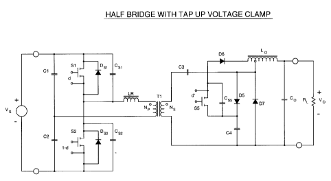
?s In the circuit of Fig. 4, a coupled tap up winding is added to inductor Lo
and diode
D6 is added in series with the winding. Switch means comprising SS and Css is
connected to the other end of this diode rather than to the cathode of diode
D7,
with the other end of the switch being connected to the common point between
DS
and the clamping capacitor C4. 'Typically the tap up winding will be S to 15%
of
CA 02270816 2003-07-24
the number of turns on the main winding of the inductor. This aspect of the
invention both reduces the time that the clamp current flows in DS and
substantially reduces the current through SS at the expense of a slightly
higher
voltage on SS when S2 is on. SS and D6 are poled to conduct current from C4 to
5 the output inductor when SS is ON.
Fig. S shows a typical circuit to create the duty cycle controlled rectangular
waveforms used to control switch S1, S2 and S3. A pulse width modulator, whose
duty cycle output is responsive to a control input, creates the waveform for
S1.
to An inverter is used to cause a complimentary waveform for switch S2. Slight
time
delays are introduced to the rising time of the two drive waveforms to allow
the
voltage in the switches S 1 and S2 to come to zero before these switches are
turned
on. Switch SS is turned on when the voltage across it is zero and turned off'
at the
same time as swit<;h S 1.
The circuit operation of the last shown embodiment (Fig. 4) being a preferred
embodiment of the invention is described following with reference to Fig. 6
and
Fig. 7, both representing full load operation.
2o The gate drive waveforms for controlled switches S 1 and S2 are shown in
Figs. 6a
and 6b respectively. They are non-overlapping complimentary waveforms with
duty cycle d and (1-d) and can be generated with the drive circuit shown in
Fig. 5.
The resulting voltage wavefonn of~ the common point of switches S 1 and S2 is
shown in Fig. 6c. This is a trapezoidal waveform with Period T, on time of Sl
Ton, and duty cycle D--Ton/T. This voltage is equal to Vs when S1 is on and
approximately Ov when S2 is on and transitions roughly linearly between these
values when both switches are off at a rate depending upon the switch currents
at
turn off and the value of Cs~ and Cs~. Both switches are turned on and off
when
the voltage across them is approximately zero. Fig. 6d shows the voltage at
the
CA 02270816 2003-07-24
11
common point of L,R and the primary of T 1 with respect to the negative
(common)
terminal of Vs. 7:'here is a delay on the positive going edge of this waveform
caused by the commutation time required to slew the current to zero in the
output
diode D7. This results in a rE:duced effective on time, Ton'. Subsequent to
this
s there is a slight overvoltage during the time clamp diode DS conducts. This
overvoltage reduces when DS finishes conducting and D6 and SS starts to
conduct.
This waveform voltage goes to approximately zero when S 1 turns off. The
voltage at the common point of C' 1 and C2 (Fig. 6c) adapts to duty cycle
changes
so that there is no DC voltage across the transformer. Thus the transformer
to primary voltage waveform (Fig. (e) is identical to Fig. 6d, but is bipolar
in nature
with no DC component. The voltage across the secondary of the transformer
(Fig.
6f) is identical to the primary voltage wavefortn except it is changed in
magnitude
by the transformer turns ratio. The voltage at the cathode of D7 with respect
to the
output circuit common (Vo-) is~ shown in Fig. fig. This waveform is the same
Is amplitude as the -transformer secondary waveform and is essentially the
same
shape but is unipolar as a result of the rectification action of D7 and DC
blocking
capacitor C3. This waveform is averaged by the output filter consisting of Lo
and
Co to create the output voltage Vo. 'fhe load Rl is connected across the
output
capacitor Co. The output voltage is proportional to the effective duty cycle
D':
zo
Ns N,s
Vo --- Vs ---- D' or Vo = Vs -- KD
Nf~ Np
2s
The commutation duty cycle loss factor K is proportional to the output current
and
is typically 0.9 or l;reater. Thus the converter is a buck derived type.
The voltage at the other end of Lo is shown in Fig. 6h. This voltage waveform
is
3o slightly larger than that at the, 1a7 cathode, due to the tap up winding,
and goes
CA 02270816 2003-07-24
12
slightly negative. (capacitor C~l is sized such that its voltage is
essentially constant
at the peak value of the D7 cathode voltage. The voltage across SS is shown in
Fig. 6i. It is an invented version of the L,o tap voltage due to the relative
connection of 55., with the negative portion of the waveform, when DS is
s conducting, blockc;d by D6. Fig. 6j shows the gate drive voltage of SS which
caused SS to turn on during the time DS is conducting and to turn off at the
same
time as S 1. Thus switch SS is also zero voltage switched.
The current wavefi~rms of this embodiment of the invention is shown in Fig. 7
also
1 o for full load condition. Fig. 7a. shows the current through the parallel
combination
of S 1 and Ds ~ . When the voltage across S 1 and Ds i becomes zero the
current
initially flows thraugh Ds~ during which time S 1 is turned on. 'The current
ramps
up quickly, flowing through S 1 when it changes polarity. Initially this
current
overshoots due to the reverse current of diode D7 during it's reverse recovery
time,
is and then ramps downward as D5 conducts until DS conduction cease, then it
ramps upwards dine to the finite inductance of Lo and magnetizing inductance
of
T 1. The current in S 1 ceases abruptly when S 1 is turned off by its gate
drive
signal (Fig. 6a). 7,he current f~awing in Lr and the primary of T1 then flows
through Cs~ and C's2, as shown in Fig. 7b, and causes the dewing of the switch
2o voltage (Fig. 6c). When the voltage across S2 becomes zero the current
ceases in
Cst and Cs2 and flaws through dliode Ds2 as shown in Fig. 7c. This current
slowly
ramps up and switch S2 is turned on before the current changes polarity. This
current increases semi-sinusaidally through S2, until it is stopped abruptly
when
switch S2 is turned off by the gate drive waveform Fig. 6b. Subsequently the
2s current through L,r and the primary of T 1 (spawn in Fig. 7c~i) runs
briefly through
Cs~ and Cs2 until Sl and Ds~ ag;ain conducts. The current through the primary
of
T 1 is a combination of the current waveforms of Fig. ?a, Fig. 7b and the
inverse of
Fig. 7c.
CA 02270816 2003-07-24
13
The current through the secondary of Tl is similar to Fig. 7d except scaled in
amplitude by the turns ratio of the transformer and minus the small
contribution of
the magnetizing current of T 1. The current through diode D7 is shown in Fig.
7e.
The current starts at zero when S2-Dsz conduct then ramps semi-sinusoidually
s upwards. It starts ~:o ramp dowvnwards when S2 turns off and ramps down more
rapidly when S 1 conducts. The current then becomes somewhat negative due to
its
inherent reverse recovery time then quickly returns to zero. This reverse
current
causes extra energ:~ to be stored in Lr which causes the voltage on the
cathode of
D7 to overshoot and DS to conduct in a triangular fashion as shown in Fig. 7f.
to When this current reaches zero, switch SS and diode D6 conduct the current
shown in Fig. 7g, which subsequently stops abruptly when SS and S1 are turned
off.
The current through the main winding Lo and the output current are shown in
Fig.
is 7h. The current through Lo is the normal output inductor current for a buck
derived converter being non-pulsating DC~' with a small triangular ripple.
The operation at lil;hter loads is similar except at typically between one
half to one
quarter full load complete zero voltage switching of S1 is lost and is
replaced by
2o partial hard-switching. 'This is not a serious drawback as the conduction
losses are
relatively small at these loads and make up for the increased switching
losses.
Switches S2 and SS zero voltage switch i:or all toads. To achieve voltage
regulation at no load the duty cycle ofd S1 is reduced towards zero. Similarly
the
duty cycle can be reduced to ~:,ffect output current limiting down to a short
circuit
2s on the output with zero voltage, :witching maintained for all controlled
switches.
As can be seen from the circuit waveforms, the converter is a buck derived
isolated converter featuring zf:ro voltage switching of the controlled
switches and
zero current switching of the output non-controlled switch and having good
CA 02270816 2003-07-24
14
components load factors. The load factor of the transformer is almost twice as
good, and the S2 and D5 load factors are only slightly inferior to that of the
active
reset forward converter. Zero voltage switching of the controlled switch is
achieved without the addition of a third controlled switch in series with the
output.
s
The converter of the present invention has been found to have an output
voltage proportional to the on t:i me of switch S 1, therefore it is a buck
derived
converter. It is ea:;y to control and regulate, has no right half plane zero
of the
buck-boost or boo;>t derived converters. It has a non-pulsating output current
and
to is relatively simple and has good component load factors, especially of the
transformer. It provides zero voltage switching of the controlled switches and
zero current switching of the output non controlled switch without using a
third
series controlled switch. The converter is suitable for medium output voltages
such
as 48 Volts or 24 'Jolts though is not suitable for low output voltages such
as SV
1s due to the presence of the capacitor in series with the transformer
secondary.
It will be appreciated by those skilled in the art that modifications to the
preferred
embodiments described herein., including electrical equivalents may be made
without departing from the principles of the invention or the scope of the
claims.
2o For example, the tap winding; of the output inductor can be realized with
two
separate coupled windings or with one winding with a tap connection. The
transformer and on.e or even botih of Lr and the output inductor could be
integrated
into one structure. A lossy type voltage clamping means for the output diode
could be employed rather than tile lossless type preferred. The polarities of
the
2s diodes and controlled switches could also be reversed on the input and/or
output
thereby allowing operation of° the circuits with negative input and/or
output
voltages. Also, additional circuit elements, well known by those skilled in
the art,
such as RC dampers on certain elements may be necessary to achieve optimum
operation of invem.ion. In addition, a saturable reactor may be added in
series with
CA 02270816 2003-07-24
the output diode to limit the reverse recovery current in the output diode
without
departing from the scope of the invention or of the claims.