Note: Descriptions are shown in the official language in which they were submitted.
CA 02271041 1999-04-30
WO 98!19391 1 PCT/DK97l00497
Pulse Modulation Power Amplifier With
Enhanced Cascade Control Method
Technical Field
This invention relates to a power amplifier for the audio
frequency range, comprising a pulse modulator, a power am-
plifier stage for amplifying the modulated signal, the out-
put of which is low pass filtered in a demodulation filter
for obtaining an analog output to feed to a consumer.
Background
Nearly all commercially available power amplifiers for fre-
quencies in the above range are of the linear analog type,
class A, AB, and B. Since the output transistors of such
amplifiers operate in the linear region, they have a low
efficiency and dissipate a considerable amount of heat. The
basic pulse modulation ("digital") switching class D power
amplifier method in theory provides a much higher effi-
ciency, which lowers the amplifier volume and heat develop-
ment. Despite this efficiency advantage, prior art in the
field has not provided solutions with an acceptable audio
quality, that could make them generally useful and direct
replacements for analog amplifiers. Accordingly, the use of
digital power amplification has been limited to applica-
tions where the demands for output quality are low. The
reasons for this will be presented in the following, when
the general prior art principles are discussed.
Prior Art
There is a fundamental requirement for efficient control
systems to eliminate errors generated in the various blocks
of the digital switching power amplifier. In the basic
digital power amplifier the input signal is modulated into
a pulse modulated signal. A switching power stage performs
amplification of the signal, and a low pass filter regen-
erates the modulated but now amplified signal. The basic
method form the basis for a range of prior art arrange-
n
CA 02271041 1999-04-30
WO 98/19391 2 PCT/DK97/00497
ments. However, there are numerous non-ideal features with
this method .
- Any modulator errors are fed directly to the load.
- Any power stage errors are fed directly to the load.
- There is no rejection of power supply perturbations.
Since the power stage output is largely proportional to the
supply voltage, any supply ripple will intermodulate with
the audio signal.
- The post filter errors will introduce further distortion,
since magnetic core materials are not ideal.
- The total output impedance is high, especially at high
frequencies, due to the filter.
- The sensitivity to load variations is high due to the
I5 passive post filter. Accordingly, changes in load impedance
will distort the frequency response of the amplifier.
- The sensitivity to temperature drift, component toler
ances, and aging effects is high. The non-controlled digi
tal switching amplifier is therefore not robust and reli
able.
Compensation for these major problems areas-is absolutely
vital, if very high fidelity is to be obtained. Prior art
methods are based on two different control methods, charac
terized by having a single feedback loop.
One basic principle is to feed back the amplifier output.
However, the poles of the iow pass filter cause a large
phase shift which puts strong restrictions on loop design.
Consequently, reasonable loop bandwidths requires high
switching frequencies. This causes several problems, such
as lower efficiency, and poor performance due to the first
two errors mentioned above.
Another basic principle of feedback in prior art, is single
loop feedback before the filter network, whereby the phase
lag of the post filter is avoided. However, the high fre-
quency content at the power stage output makes the feedback
CA 02271041 1999-04-30
WO 98/19391 3 PCT/DK97/00497
source potentially very noisy. Furthermore, a number of the
above errors are not (or only partially) compensated .
The fundamental problem of both methods are the conflicting
desires for a low carrier frequency, high gain-bandwidth
product and good stability characteristics in all situa-
tions. A further problem with prior art arrangements is the
apparent complexity of the system, partially caused by in-
efficient control.
The following publications are relevant as background mate-
rial and illustration of the methods and the problematic
issues of three prior art arrangements:
[1] Suzuki, T. . Pulse Width Modulated Signal Amplifier. US
Patent no. 4021745 (1977)
[2] Yokoyama, K. . Pulse-Width Modulation Circuit. US Pat-
ent no. 4531096 (1986)
[3] Attwood, B.E. . Design Parameters Important for the
Optimization of Very High-Fidelity PWM (Class D) Audio Am
plifiers , Journal of the AES, Nov. 1983. p. 842-853.
[4] Taylor, W.E. . Digital Audio Amplifier . US Patent.
No. 4724396 (1988).
[5] Hancook, J. . A class D Amplifier Using MosFET's with
Reduced MinorityCarrier Lifetime , 89t'' Convention of the
AES. Los Angeles. CA. September 21-25. 1991.
[61 Solomon, E.E . Digital Power Amplifier. US Patent No.
5126684 (1992).
[7] McCorkle, D.P. Class D amplifier. European Patent.
Publ. No. 557032A2 (1993).
[8] Nakajima, Y. Pulse-Width Modulation amplifier. European
Patent. Publ. No.503571A1 (1993).
[9] Leigh, S.P et al. Distortion analysis and reduction in
a completely digital PWM class D power amplifier, Interna
tional Journal of Modeling & Simulation, Vol. 14, No. 2,
1994.
i~
CA 02271041 1999-04-30
WO 98/19391 4 PCTIDK97100497
OBJECTIVES
According to the above stated problems that exist with
prior art arrangements, the primary objective of the pres-
ent invention is to provide a pulse modulation amplifier
which can deliver very high power outputs, and still pro-
vide ultra low distortion (less than 0.01%) and noise (less
than 100~V RMS), and yet a very high efficiency (90-95%)
and low idle losses.
Another objective of the invention is to maintain low com-
plexity by avoiding the use of advanced but complex and
hence potentially unreliable circuitry, and also to elimi-
nate the requirement for tuning in production.
Another important objective of the invention is to elimi
nate the need for a stabilized supply, meaning that a sim
ple non-regulated bridge rectifier with a stabilizing ca
pacitor is sufficient. In this way, a minimal complexity
and maximal efficiency is secured from the mains input to
the amplifier output terminals.
The final objective of the invention is to obtain minimal
sensitivity to load variations, and furthermore to provide
robustness and reliability.
SUb~SARY OF THE INVENTION
The above objectives are obtained with the present inven-
tion. In the first preferred embodiment, an amplifier ac-
cording to the invention is particular in that negative
feedback is introduced from the switching power stage out-
put to one or several loops feeding into one or several
pre-amplifier stages preceding the modulator. This offers a
range of advantages that are new to the art, in terms of
performance and stability control. A further embodiment of
the invention is particular in that the local feedback has
a enhanced cascaded structure with a single feedback path,
that comprises a filter with a phase characteristic such
that a pole in the demodulation filter is compensated.
CA 02271041 2002-08-14
Another embodiment of the invention is particular in that
further feedback is established from the output of the de-
modulation filter to one or several pre-amplifier stages,
5 so that the pulse modulation ("digital") switching power
amplifier circuit elements are enclosed by an enhanced cas-
cade structure of feedback loops, providing further im-
proved performance and stability control.
A further embodiment of the invention is particular in that
the pulse modulator is a controlled self-oscillating modu-
lator comprising a non-hysteresis comparator for pulse
modulation, and a higher order oscillating loop realized by
means of two poles, preferably a pole in the first (local)
forward path and feedback path. This provides en extremely
simple and stable configuration, obviating the need for a
separate carrier frequency generator.
A further embodiment of the invention is particular in that
the pulse modulator is a carrier based modulator. This
means that well-known design techniques for carrier based
modulators may be used in the configuration according to
the invention.
A further advantageous embodiment of the invention when
carrier based modulation is used, is particular in that a
notch filter is provided in the single feedback path block
between the amplifier and the loops. Thereby it is possible
to simplify the filtering out of the carrier frequency in-
fluences on the system performance in carrier based sys-
tems. A similar result is obtained in a further advanta-
geous embodiment of the invention which is particular in
that a structure creating a high frequency pole is provided
in the feedback path block.
CA 02271041 2002-08-14
Sa
The invention also prov_i.des avulse modal Lation power amplifier
for the audio frequency range, comp.ri.ain<~ a p~zlse modulator,
and a switching stage Eor amplifying true modulated signal,
the output. of which is low L>ass t::i..l.ta:~red in a demodulation
S filter for obtaining an analog output to feed to a consumer,
wherein a first. negative feedbac::k 1:r> itutroduced from the
switching stage output to one or ~;everal feedback loops
feeding into one or ss=veral forw<xr~~l piths preceding the
modulator, at least one of the feedbuc:,k loops comp .risi.ng a
1o f.=_edback path with a phase characteristic- such that a pole
in the demodulation filter .is c:ompc_nsatE>d.
The invention also provides a pu lse rnoclulation power
amplifier for the audio frequency range, comprising a pulse
15 modulator, and a swit~~hinr~ stage for amplifying the
modulated signal, the output of whic,tn is low pass filtered
in a demodulation filter for obtaining am analog output to
feed to a consumer, wherein a first nec~atiiTe feedback is
introduced from the switching stage output to one or several
2o forward paths preceding the modulator, anc~ wherein a second
feedback is established from the output of the demodulation
filter to one or several forward paths.
The invention also provides a controlled self-oscillating
25 modulator comprising a non-hysteres is cornparator foxy pulse
modulation of a switching stage, and <~ vc>ltage feedback loop
from the switching stage to the compaz~ctor, the feedback
lc>op securing stable oscilating corrditioris by means of at
least two poles, wherein the feedback loop comprises a
3o feedback p<~th providing a feedback si.gr~al to a forward path,
the feedback signal bein<~ superposed with a reference signal
in the forward path, the feedback path ~::,pmprising at least
ore pole, and the forward pazt:h comprising a,t least one pole.
35 BRIEF DESCRIPTION OF THE DRAWINGS
The invention wil.L be further described with reference to
the drawings, in which,
i
CA 02271041 1999-04-30
WO 98/19391 6 PCT/DK97I00497
Fig. 1 shows the principle in prior art conventional pulse
modulation ("digital") switching power amplifiers
Fig. 2 shows a prior art method with single loop feedback
based on the overall amplifier output as the feedback
source
Fig. 3 shows a prior art single loop feedback with power
stage output as the feedback source
Fig. 4 shows the a general block diagram of a first embodi-
ment of the present invention, a digital switching ampli-
fier improved by an Multivariable Enhanced Cascade Control-
ler (MECC) based on single feedback from the switching
power stage output.
Fig. 5 shows a general block diagram of a second embodiment
of the present invention,
Fig. 6a and 6b exemplify general recursive loop synthesis
methods for the first (Fig. 6a) and second (Fig. 6b) em-
bodiments of the invention.
Fig. 7 shows a detail of a preferred embodiment of single
feedback MECC.
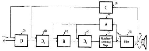
Fig. 8 shows a detail of a preferred example of the second
embodiment of the invention, the dual feedback Multivari
able Enhanced Cascade Controller (MECC).
Fig. 9a and 9b show the loop characteristics for the two
preferred examples of the first two embodiments of the pre-
sent invention, shown in Fig. 7 and Fig. 8.
Fig. 10 illustrates the third embodiment of the present in-
vention, the controlled self-oscillating pulse modulator
characterized by a non-hysteresis comparator and additional
CA 02271041 1999-04-30
WO 98/19391 7 PCTIDK97/00497
poles in the first local loop to secure self-oscillating
conditions
Fig. 11 shows essential signals of the third embodiment of
the invention, the controlled oscillating pulse modulator.
Fig. 12 illustrates the principle of a fourth embodiment of
the invention, an alternative three-level pulse width modu-
lator for implementation with a 4 transistor bridge power
stage. The signals are from top to bottom . Modulating sig-
nals, normalized voltage on each phase in a bridge power
stage (A, B), and finally both the normalized differential
and common mode output signals (A-B and A+B). The differ-
ence signal is fed to the load.
Fig. 13 illustrates the spectral characteristics of the al-
ternative three-level modulator. The output amplitude spec-
trum is shown OdB and -60dB relative output levels.
Fig. 14 (a)-(c) illustrate various performance specifica
tions for an implemented example embodiment of the inven
tion with a 250W maximal power handling capability. Fig. 13
(a) shows power efficiency. At 250kHz switching frequency
the efficiency approaches 920, and with 50kHz switching
frequency the efficiency approaches 96%.
Fig. 14 (b) shows the very low measured Total harmonic dis-
tortion + Noise (THD+N) vs. output power at 100Hz, lKHz and
lOKHz (top curve).
Fig. 14c (c) shows the measured amplifier noise. The noise
floor at -150dB corresponds to an RMS noise level of only
70~.V.
DETAILED DESCRIPTION
The basic "digital" power amplifier is shown in Fig. 1. The
input signal is modulated (11) into a pulse modulated sig-
nal. A switching power stage (12) performs amplification of
i~
CA 02271041 1999-04-30
WO 98!19391 g PCT/DK97100497
the modulated signal, and a low pass filter (13) regener-
ates the audio waveform.
A first category of prior art control principle is shown in
Fig. 2. This displays the basic problems: that a reasonable
gain- bandwidth product requires very high switching fre
quencies due to post filter phase lag and the lack of local
correction schemes. Reasonable gain-bandwidth product at
all frequencies within the amplifier bandwidth is impossi
ble to obtain.
Fig. 3 shows a second category of prior art control princi-
ples which displays the following basic problems: noisy
feedback source, no post filter error correction, load sen-
sitivity and limited loop gain-bandwidth product caused by
single loop control.
Fig. 4 illustrates the first embodiment of the invention.
The basic pulse modulation ("digital") switching power am-
plifier circuit elements are enclosed by an enhanced cas-
cade (or nested) structure of feedback loops. This first
embodiment is termed a (single feedback) Multivariable En-
hanced Cascade Controlled (MECC) digital power amplifier.
The control structure is characterized first by having a
single feedback source and second by a single feedback path
A (7) having a lowpass characteristic. The control struc-
ture is simple in implementation since it consists of a
single feedback path A and a set of forward path blocks Bi.
Using preferred loop design procedures, each loop has a
very stable 1st order characteristic and the forward path
blocks are preferably simple. MECC offers a range of advan-
tages that are new to the art:
- A higher order control system combined with a high level
of stability and robustness, since each loop considered in
dividually is very stable.
- The enhanced cascade control method provides hitherto un-
CA 02271041 1999-04-30
WO 98119391 g PCTIDK97/00497
known freedom in loop design and optimization possibihi-
ties. Thus, the equivalent loop gain bandwidth at any fre-
quency can as such be increased infinitely relative to sin-
gle loop systems without compromising stability.
- The lowpass characteristic of the feedback path provides
a closed loop zero-pole lead characteristic that can be de-
signed to cancel one of the filter poles . The result is a
much improved system for global feedback.
- Each loop individually reduces the sensitivity to power
stage errors and improves system performance (distortion,
noise...) by a factor corresponding to the loop gain. MECC
provides an equivalent feedback corresponding to the prod
uct of contributions of each loop.
- Successive improvement by multiple loops is more effi-
cient than in a one loop realization.
- Frequencies of unity loop gain in each loop can be re-
duced compared to single loop system, while still providing
improved performance. Thus, the switching frequency can be
reduced.
- MECC has low requirements for dynamic range of the indi-
vidual compensator blocks A and Bi . Using preferred design
procedures, the signal levels throughout the control system
will have a level similar to the input signal.
The second embodiment of the invention involves the exten-
sion of the first embodiment to a dual feedback Multivari-
able Enhanced Cascade Control (MECC)structure, were the two
cascades are closely connected. A general block diagram is
illustrated in Fig. 5. The system relies on the zero-pole
lead characteristic caused by the single lawpass feedback
path of the local enhanced cascade. Dual feedback MECC pro-
vides further improvements to the system. The system band-
width is increased beyond the demodulation filter bandwidth
i~
CA 02271041 1999-04-30
WO 98119391 10 PCTlDK97J00497
limit. This minimizes phase and amplitude distortion within
the audio band. Furthermore, the transient response is im-
proved. Post filter errors are corrected, meaning that the
requirements for filter inductor linearity is low. Further-
more, the output impedance is reduced considerably, and so
is the sensitivity to load variations.
A third embodiment of the invention is a forced self-
oscillating pulse width modulator, characterized by first a
non-hysteresis comparator as a modulator and secondly by a
higher order oscillating loop realized with both forward
path B1 and feedback path A to determine self-oscillating
conditions.
A fourth embodiment of the invention is an alternative car-
rier based three-level pulse width modulator with attrac-
tive characteristics in combination with MECC.
Further embodiments of the invention include .
- Means for obtaining improved elimination of noise from
the noisy feedback by using a notch filter and high fre-
quency poles in the local feedback or alternatively forward
path. This improves distortion when carrier based pulse
width modulation is used.
- Means for compensating for large scale power supply regu-
lation, in order to obtain improved stability and effi-
ciency improvements at all output levels. This is relevant
with carrier based modulation, where the gain of modulator
and power stage is dependent on the power supply rail
level, meaning that the power supply perturbation may in-
fluence stability unless such precautions are taken.
DESCRIPTION OF THE FIRST EMBODIMENT
The enhanced cascade control method new to the art relies
on the fact that the modulator and amplifier can be repre-
sented by a constant gain Kp over a wide bandwidth. One
CA 02271041 1999-04-30
WO 98!19391 11 PCTJDK97/00497
general recursive approach to design the local cascade is
illustrated in Fig. 6a. The feedback path has a lowpass
characteristic:
A(s) -= 1 1
K Tl s+1 (1)
The lowpass characteristic of the feedback path is benefi-
cial in several aspects. It causes a closed loop zero-pole
phase lead characteristic which can be very useful for re-
alizing a cancellation of one of the poles of the demodula-
tion filter. Furthermore, the pole causes an important fil-
tering of the high frequency switching noise from the power
stage output, which is essential when carrier based modula-
tion methods are used (the fourth embodiment of the inven-
tion). In this simple examplary embodiment the initial for-
ward block is a simple gain, with a gain that leads to a
constant open loop and closed loop gain of K in the fre-
quency band of interest:
B1 (s~ - K r!
Kp r2 (2)
Whereas the i~th block has a pole-zero characteristic to
compensate for the zero-pole characteristic of the preced-
ing loop:
B1 (s) -_ Z1 z
t2 Zls+1 (3)
By this realization the open loop gain of the single loop
configuration can be written by the following 1. order ex-
pression:
i~
CA 02271041 1999-04-30
WO 98119391 12 PCTIDK97/00497
HLl,oi (s) = K p A(s)B(s)
K _1 1 K z1
p K z1 s+1 Kp z2 (4)
_ 1 _z1
zls + 1 z2
It is easy to show that for all loops:
z1 1
HL;,o! (s) = HLl,ol (s) - z2 zls + 1 ( 5 )
The closed-loop transfer function can be approximated to:
zls+1
HL;.cI(s)=K z2s+1 (6)
By this specified simple loop synthesis procedure, each
loop will exhibit identical and stable 1st order behaviour
as illustrated in Fig. 6a.
Numerous alternative approaches to loop synthesis can be
devised. The recursive design procedure specified above
provides a frequency independent loop gain at all frequen-
cies within the target bandwidth, irrespective of the num-
ber of cascaded loops and the loop unity gain frequency.
Instead of a constant loop gain, each loop can realize e.g.
an integrator. Alternatively, each loop can be designed us-
ing two pole compensation. Both methods lead to a consid-
erabiy higher but frequency dependent loop gain within the
frequency band of interest.
Alternative variants of single feedback MECC power ampli-
fier include the use of alternative different feedback
paths A, which are optimized in respect to noise attenua-
tion , which is essential in systems where carrier based
modulation is used. If HF components related to the switch-
ing frequency were to reach the modulator, it would be im-
CA 02271041 1999-04-30
WO 98/19391 13 PCTIDK97/00497
possible to obtain a pulse width according to the instanta-
neous amplitude of the audio signal. By introduction of a
notch filter, the first critical component and intermodula-
tion components can be eliminated. The specific placement
of the notch filter in the feedback path effectively elimi-
nates the switching fundamental in all loops. By further
addition of a high frequency pole in block A, a 2nd order
attenuation characteristic of the higher order harmonics of
the switching frequency in the feedback path is realized,
and the noise attenuation is thereby further improved. A
further advantage of placing the noise attenuating cir-
cuitry in the feedback path is, that it will only have a
local effect for each loop, if the unity loop gain fre-
quency and switching frequency are properly chosen. The
noise elimination circuitry operates well above unity loop
gain, and does therefore not influence the closed loop be-
havior of any of the loops.
DESCRIPTION OF T8E SECOND PREFERRED EMBODIMENT
The second embodiment of the invention involves the exten-
sion of the first embodiment to a dual feedback Multivari-
able Enhanced Cascade Control (MECC)structure, were the two
cascades are closely connected. A general block diagram is
illustrated in Fig. 5. The system relies on the zero-pole
lead characteristic caused by the single lowpass feedback
path of the local enhanced cascade. Due to the use of two
feedback sources, this embodiment is termed Dual feedback
Multivariable Enhanced Cascade Control. The second cascade
has the same special characteristics as the first cascade
with only one single feedback path C and a set of forward
path blocks Di. One preferred approach of dual feedback
MECC design is based on the local enhanced cascade in Fig.
6a and illustrated in Fig. 6b. The main reconstruction fil-
ter F(s) is assumed to be 2. order. The feedback path has a
constant gain characteristic:
i~
CA 02271041 1999-04-30
WO 98119391 1~ PCTIDK97I00497
C(s) 1 ( 7 )
K
The initial block forward block D1 is a simple gain block
with a gain in the frequency band of interest .
D(s) - y
z3 (8)
Whereas the i~th forward block has a pole-zero characteris-
tic .
D, (s)-T1 z3s+1
r3 rls+1 (9)
By this simple recursive design procedure, each loop will
exhibit identical behavior, which is illustrated by both
the open loop HG~,oL(s) and closed loop characteristics
HGj,~L(s) in Fig. 6b:
1
HGl,ol (s) = HGl.ol (s) = T3 (zls + 1)(z2s + 1) ( 10 )
The closed-loop transfer function can be approximated to .
K
HG~,~I (s)
(r3 s + 1)(z2s + 1) ( 11 }
It should be emphasized, that the given design approach is
mainly illustrative, and that there are numerous possible
extensions which will be apparent to the skilled person,
a . g . a first order characteristic in each loop to improve
correction for errors at lower frequencies.
To maximize the robustness of the dual feedback MECC Digi-
tal power amplifier, the number of global loops should be
minimized and preferably only one global loop should be
CA 02271041 1999-04-30
WO 98/19391 15 PCT/DK97/00497
used. Tuning towards the desired distortion and noise char
acteristics should be carried out by adjusting the number
of local loops, since the dominating errors are introduced
in the switching power stage block, and should therefore be
corrected locally.
A fundamental advantage of the powerful Multivariable En-
hanced Cascade Control method in both embodiments is, that
design of modulator, power stage, post filter and power
supply can be relaxed considerably without compromising
audio performance. These fundamental elements can be imple-
mented with simple standard components and thereby have a
low cost and complexity.
The control method comprising first and embodiment of this
invention functions independently of the pulse modulator
and power stage realization. The only requirement for the-
ses two blocks is that they realize an amplification of the
analog modulator reference input over a frequency range
that is wider that the desired bandwidth. Thus, the modula-
tion may be single sided or double sided, two level or mul-
tilevel pulse width modulation, or even alternative modula-
tion schemes such as Sigma-Delta modulation.
THE THIRD EMBODIMENT OF THE INVENTION
A further preferred embodiment regarding modulator imple-
mentation for the MECC digital power amplifier is a Con-
trolled self-Oscillating Pulse Modulator, new to the art.
An example of an embodiment realizing this method is shown
in Fig. 10. The preferred method is characterized by having
a non-hysteresis comparator as a modulator and by modifying
the first local loop to a have higher order characteristic,
by an additional pole in both forward path block B1 and
feedback path A. This secures controlled and stable self-
oscillating conditions. The desired pulse modulation effect
is then obtained by superposing the oscillating signal with
the signal input (Vi). Fig. 11 shows an example of the sig-
i~
CA 02271041 1999-04-30
WO 98!19391 PCTIDK97/00497
16
nal characteristics at the reference point for the modula-
tor where the oscillating signal is superposed with the in-
put signal. Furthermore, the pulse modulating effect is
shown.
Advantages of the above described Controlled self-
Oscillating Pulse Modulator over constant frequency carrier
based methods are several. First, the modulator is ex-
tremely simple to implement since no carrier generator is
needed. Secondly, the bandwidth of the unity gain frequency
of the first local loop is the oscillation frequency lead-
ing to wide bandwidth control even with modest switching
frequencies. Third, power supply rail no longer determines
the equivalent gain of the modulator/power stage meaning
that large scale power supply perturbation is automatically
cancelled, and does no longer influence stability in other
loops in the enhanced cascade structure. -The unity gain
frequency of the local loop is inherently determined by the
frequency of positive feedback, i.e. the control loop band-
width is considerably wider than in traditional carrier
based systems, where a rule of thumb is a factor of three
between unity gain frequency and carrier frequency.
OTHER EMBODIMENTS
Other embodiments of the of invention include the use of
pulse width modulation, preferably with three discrete am-
plitude levels. To aid in this understanding this alterna-
tive embodiment regarding modulator implementation, Fig. 12
illustrates the essential time domain waveforms and Fig. 13
the frequency domain spectral amplitude characteristics.
From Fig. 12 it is obvious that by using three-level PWM
the effective sampling frequency is doubled since there are
two samples pr. switch cycle. This is obtained without in-
creasing the power losses, since each transistor operates
at a rate equal to the switching frequency. Accordingly,
three-level PWM allows the loop bandwidths to be increased
or alternatively the switching frequency to be decreased.
CA 02271041 1999-04-30
WO 98/19391 1,~ PCTIDK97/00497
A further embodiment of the invention relates to the case
where MECC is combined with constant frequency carrier
based modulation, and is characterized by the design change
described hereinafter. Improved means to compensate for any
large scale variations of the power supply voltage is ob-
tained by intelligent automatic gain adjustments in the
first local loop. The equivalent gain of the modulator and
power stage, KP, is largely proportional to the power sup-
ply voltage. Accordingly, the gain of ~1 should be regu
laced inversely proportional to the supply voltage varia
tion:
K z1
B1 ~KP ) = KP z2 C 12 )
This design change will have a further stabilizing effect
on the digital power amplifier based on MECC since the
characteristics of the first loop will be independent power
supply perturbations. Large perturbations of the power sup-
ply voltage will not influence stability. The adaptive ad-
justment of the power supply allows an intelligent control
of the power rail voltage e.g. controlled by the volume
control without compromising stability. This can be util-
ized to secure optimal efficiency at all output levels.
Further embodiments include additional secondary filtering
circuitry on the amplifier output for further elimination
of switching components, and the addition of an input fil-
ter to shape the overall amplifier response in- frequency
and time.
EXAMPLES OF THE FIRST AND SECOND EbIBODIMENT
Fig. 7a and 7b show more specific double loop examples of
both the single and dual feedback MECC embodiments. The de-
sign procedure of each loop is given in Fig. 9a and 9b re-
spectively. Compared with the general design procedure, the
i~
CA 02271041 1999-04-30
WO 98119391 PCT/DK97/00497
18
LF performance has been optimized such that the equivalent
loop gain in both loops is significantly increased at lower
frequencies compared to the general approach. Table 1 gives
example parameter values relative to the amplifier band
s width.
Table 1
Parameter Frequency (rel. to bandwidth)
1/z1 2
I / z2 10
IlzLp 1/5
The enhanced cascade provides a significant improvement
over a the single loop approaches known in the art, with
only a marginal increase in system complexity in terms of
the added forward block BZ. Provided that the reconstruc-
tion filter is reasonably linear, the local feedback MECC
embodiment can realize high end specifications. Further im-
provement may be realized by adding blocks equal to B2. Al-
ternative use of this first embodiment of the invention is
to drive loudspeakers directly without reconstruction fil-
ter.
Fig. 7b provides an example of an embodiment of dual feed-
back Multivariable Enhanced Cascade Control (MECC) with one
local and one global loop, both closely connected. Compared
to the general design procedure specified in Fig. 6 both
loops have been LF optimized to significantly increase the
loop gain in both loops at lower frequencies. Table 2 gives
examples of parameter values relative to the amplifier
bandwidth.
CA 02271041 1999-04-30
WO 98/19391 1g PCT/DK97/00497
Table 2
Parameter Frequency (rel. to bandwidth)
1/z1 2
1/z2 10
1/z3 4
1I zLp 1~5
In order to clarify the significant advantages of the dual
feedback MECC digital power amplifier over prior art, the
embodiment in Fig. 8 has been implemented in two higher
power examples, one to cover the full audio bandwidth of
20kHz utilizing a 250kHz switching frequency, and one exam
ple covering a reduced bandwidth of 4kHz, utilizing a 50kHz
switching frequency.
It should be emphasized that the chosen parameters are only
illustrative, and that the MECC digital power amplifier is
well performing on a much wider range of output powers and
bandwidths. Figs. 14 (a) - (c) illustrate various key
specifications for the given example, and the results ob-
tained are summarized in Table 3. If further improvements
are desired, one preferred approach is to use a double lo-
cal loop by simple addition of a B forward block.
i
CA 02271041 1999-04-30
WO 98119391 2 0 PCT/DK97/00497
Table 3
Specification Measurement
Max. power 250W
Bandwidth 20kHz / 4kHz
THD+N (lKHz, 1W) <0.01%
THD+N (20Hz-20KHz) <0.05%
Intermodulation dis- <0.01%
tortion (IMD)
Idle noise (RMS) 70~.V
within bandwidth
Dynamic range 115dB
Power Stage Efficiency 92% / 96%
(250kHz / 50 kHz
switching frequency)
In general no prior art approach yields a comparable combi-
nation of fidelity, efficiency, and low complexity.