Note: Descriptions are shown in the official language in which they were submitted.
CA 02271102 1999-OS-06
WO 98I20605 PCT/GB97/03081
, - 1 -
A RESONANT POWER CONVERTER FOR ENERGISING A COIL
BACKGROUND TO THE INVENTION
THIS invention relates to a resonant power converter.
A square wave current signal is a preferred type of transmitted signal for
making broadband transient decay measurements which, for instance, are
used in airborne electromagnetic prospecting systems. A conventional
voltage source inverter having transistors and anti-parallel diodes produces
an essentially triangular or exponential current waveforms, and is not the
best suited for the application. The current source inverter is better used
for
this type of application, and has been described in E E Ward, "Inverter
suitable for operation over a range of frequency", Proc. IEE, Vol. 111,
August l964. A current source inverter typically requires switches with
reverse blocking capability and one or more capacitors in parallel to the
load. Forced commutation is generally also a feature of such a circuit, as a
result of which thyristors are also required.
In Canadian patent 1064584, a pulse generator is disclosed for airborne
electromagnetic prospecting. A coil is energised with periodic bipolar
' current pulses of predetermined amplitude, period and repetition rate and of
generally square waveform. A capacitor is connected in parallel to the coil
to form a closed oscillatory circuit of predetermined frequency. The
oscillatory circuit is controlled via first and second pairs of controlled
rectifiers or alternatively connecting and disconnecting the oscillatory
circuit
SUBSTITUTE SHEET (RULE 26)
CA 02271102 1999-OS-06
WO 98I20605 PCT/GB97/03081
- 2 -
from the direct current source and for alternately reversing the direction of
flow of current from the direct current source to the coil during successive
current pulses. The square wave generated by the pulse generator is
relatively inflexible, in that it is only capable of making use of the fixed
amplitude and frequency components at a given pulse repetition rate making
up the square waveform.
One type of voltage source inverter circuit arrangement where a low value
capacitor is placed at the input of a transistor inverter is described by J
He,
N Mohan and B Wold in "Zero-voltage-switching PWM inverter for high-
frequency AC-DC power conversion", IEEE Transactions on Industry
Applications, Vol. 29, No. 5, September/October 1993, pp 959-968. In this
circuit, it is not possible for the resonant capacitor voltage to become
larger
than the source voltage. In addition, resonance does not take place between
the load and the resonant capacitor, but rather between the capacitor and an
auxiliary inductor.
In a further circuit by A Hava, V Blasto and T A Lipo, described in "A
modified C-dump converter for variable reluctance machines", 1991 IEEE
IAS Conference Record, pp 886-891, unipolar pulses are provided for the
windings of a reluctance motor. A smaller capacitor is provided which does
not resonate with the load, and the diode in series with the voltage source
is not connected to the DC side of the inverter, but rather directly to the
load
windings.
In applications such as airborne electromagnetic prospecting, it is desirable
for there to be relatively flexible control of the electromagnetic signal
emanating from the coil or loop.
SUBSTITUTE SHEET (RULE 26)
CA 02271102 1999-OS-06
WO 98I20605 PCT/GB97/03081
- 3 -
In US patent 4410926 a circuit is disclosed for generating DC magnetic
fields of alternating polarity. A low value capacitor which can resonate with
the load is placed at the input of an inverter. However, the wave shape
control is very limited and does not give the flexibility which is required
for
new generation geophysical detection systems. The polarity changes are
invariably implemented using relatively slow half wave resonant transitions
and the current amplitude is not actively controlled.
SUMMARY OF THE INVENTION
According to a first aspect of the invention there is provided a pulse
generator for energizing a coil with periodic bipolar current pulses having
a generally square waveform comprising bipolar transition intervals defining
successive edges of unipolar current pulse intervals of alternating frequency,
the pulse generator comprising a resonant DC to AC converter circuit
including a DC input and an output coupled to the coil, a control circuit for
controlling the switching of the converter, a resonant capacitor connected in
parallel across the DC input, and decoupling means for decoupling the
resonant capacitor from the DC input when the voltage across the resonant
capacitor exceeds that of the DC input, the converter fiurther including first
and second resonant charging sub-circuits in which the capacitor is connected
to the coil for allowing the amplitude of the coil current to increase, first
and
second resonant discharging sub-circuits in which the capacitor is connected
to the coil for allowing the amplitude of the coil current to decrease, first
' and second freewheeling sub-circuits in which the resonant capacitor is
effectively isolated from the coil and a short circuit current path is
provided
for allowing the amplitude of the coil current to gradually decrease, and an
SUBSTITUTE SHEET (RULE 26)
CA 02271102 1999-OS-06
WO 98I20605 PCT/GB97103081
_ _
exponential charging circuit in which the DC input is connected directly to
the coil so as to allow for a rise in current through the coil, the control
circuit being arranged to control the amplitude and frequency content of the
square waveform by switching the converter circuit to operate between at
least two of the above sub-circuit types in at least one controlled switching
cycle during the unipolar current pulse intervals.
The invention further provides a pulse generator for energizing a coil with
periodic bipolar current pulses having a generally square waveform
comprising bipolar transition intervals defining successive edges of unipolar
current pulse intervals of alternating frequency, the pulse generator
comprising a resonant DC to AC converter circuit including a DC input and
an output coupled to the coil, a control circuit for controlling the switching
of the converter, a resonant capacitor connected in parallel across the DC
input, and decoupling means for decoupling the resonant capacitor from the
DC input when the voltage across the resonant capacitor exceeds that of the
DC input, the converter circuit further including first and second resonant
charging sub-circuits in which the capacitor is connected to the coil for
allowing the amplitude of the coil current to increase, first arid second
resonant discharging sub-circuits in which the capacitor is connected to the
coil for allowing the amplitude of the coil current to decrease, an
exponential
charging circuit in which the DC input is connected directly to the coil so
as to allow for a rise in current through the coil, and a clamping circuit
shunted across the DC voltage source, the clamping circuit being arranged
to supply a substantially constant DC voltage to the coil which is higher than
that of the DC input.
Preferably, the pulse generator inciudes first and second freewheeling sub-
SUBSTITUTE SHEET (RULE 26)
CA 02271102 1999-OS-06
W098/20605 PCTIGB97/03081
- 5 -
circuits in which the resonant capacitor is effectively isolated from the coil
and a short circuit current path is provided for allowing the amplitude of the
coil current to gradually decrease, the control circuit being arranged to
control the amplitude and frequency content of the square waveform by
switching the converter circuit to operate between at least two of the sub-
circuit types in at least one controlled switching cycle during the unipolar
current pulse intervals.
Conveniently, the control circuit is arranged to control the amplitude and
frequency content of the square waveform by switching the converter circuit
to operate between at least three of the above sub-circuit types in at least
one
controlled switching cycle during the unipolar current pulse intervals.
Advantageously, the converter comprises a full bridge inverter having first
and second switching arms, the first switching arm having first and second
controlled switches and the second switching arm having third and fourth
controlled switches, with first, second, third and fourth diodes being
connected in anti-parallel across the respective first, second, third and
fourth
controlled switches to provide corresponding first, second, third and fourth
switch-diode pairs.
Typically, the first resonant charging sub-circuit comprises the first
controlled switch, the coil, the third controlled switch and the resonant
capacitor, and the second resonant charging sub-circuit comprises the second
controlled switch, the coil, the fourth controlled switch and the resonant
capacitor, and the first resonant discharging sub-circuit comprises the second
diode, the coil, the fourth diode and the resonant capacitor, and the second
resonant discharging sub-circuit comprises the third diode, the coil, the
first
SUBSTITUTE SHEET (RULE 26)
CA 02271102 1999-OS-06
WO 98/20605 PCT/GB97/03081
- 6 -
diode and the resonant capacitor.
The first freewheeling sub-circuit may comprise the first controlled switch,
the coil, and the fourth diode, and the second freewheeling sub-circuit
comprises the second controlled switch, the coil, and the third diode.
The clamping circuit preferably includes a clamping capacitor and switching
means for controlling the ,operation of the clamping capacitor, the capacitor
being sized to supply the substantially constant DC voltage.
Typically, the clamping circuit forms part of a fast exponential charging
circuit for charging the coil, and a fast exponential discharging circuit for
discharging the coil into the clamping capacitor.
Conveniently, the fast exponential charging circuit comprises the clamping
capacitor, a fifth controlled switch forming part of the switching means, the
first switch, the coil and the third switch.
Typically, the fast exponential discharging circuit comprises a fifth diode in
anti-parallel with the fifth controlled switch, the clamping capacitor, the
second diode, the coil and the fourth diode.
Advantageously, the fast exponential charging and fast exponential
discharging circuits are arranged to operate during the bipolar transition
interval, in combination with the resonant charge and discharge circuits.
According to a further aspect of the invention there is provided a method of
generating a series of periodic bipolar current pulses having a generally
SUBSTITUTE SHEET (RULE 26)
CA 02271102 1999-OS-06
WO 98I20605
PCT/GB97/03081
square waveform comprising bipolar transition intervals defining successive
edges of unipolar current pulse intervals of alternating frequency, by using
a resonant DC to AC converter having a DC input, an output coupled to a
coil, and a resonant capacitor connected in parallel across the input and
arranged to form a resonant circuit in conjunction with the coil, the method
including the steps of controlling the amplitude and frequency content of the
square waveform by operating the pulse generator in a resonant charging
mode, in which the resonant capacitor is connected to the coil for allowing
the amplitude of the coil current to increase, a resonant discharging mode in
which the capacitor is connected to the coil for allowing the amplitude of the
coil current to decrease, an exponential charging mode, in which the DC
input is connected directly to the coil, and a freewheeling mode in which the
resonant capacitor is effectively isolated from the coil and a short circuit
current path is provided for allowing the amplitude of coil current to
gradually decrease.
Preferably, the method includes the step of operating the pulse generator in
a fast charging mode in which the coil is charged via a clamping circuit
which is connected in parallel across the DC input; and is arranged to supply
a substantially constant DC voltage which is higher than the DC input, and
a fast exponential discharging mode in which the coil discharges into the
clamping circuit.
Advantageously, the method includes the step of clamping the coil voltage,
operating the pulse generator in the fast discharging mode by commutating
the coil current to the clamping circuit, and subsequently operating the
clamping circuit in the fast charging mode when the polarity of the clamping
current changes.
SUBSTITUTE SHEET (RUL,E 26)
CA 02271102 1999-OS-06
WO 98I20605 PCT/GB97/03081
_ g _
Conveniently, the method includes the steps of providing at least one
controlled switching cycle during each unipolar pulse interval, each
switching cycle including a charging interval, and a discharging interval
corresponding to the aforesaid modes.
Typically, each switching cycle further includes fast exponential charging
and discharging intervals.
Conveniently, each switching cycle also includes slow exponential charging
and discharging intervals.
Typically, two to five switching cycles are provided, with each cycle being
a PWM-controlled cycle.
Advantageously, the method includes the steps of operating the pulse
generator, during each bipolar transition interval, in at least the resonant
charging and resonant discharging modes.
According to a still further aspect of the invention there is provided a
method of generating a series of periodic bipolar current pulses having a
generally square waveforrn comprising bipolar transition intervals defining
successive edges of unipolar current pulse intervals of alternating frequency,
by using a resonant DC to AC converter having a DC input, an output
coupled to a coil, and a resonant capacitor connected in parallel across the
input and arranged to form a resonant circuit in conjunction with the coil,
the method including the steps of controlling the amplitude and frequency
content of the square waveform by operating the pulse generator in a
resonant charging mode, in which, the resonant capacitor is connected to the
SUBSTITUTE SHEET (RULE 26)
CA 02271102 1999-OS-06
WO 98/20605 PCTlGB97/03081
- 9 -
coil for allowing the amplitude of the coil current to increase, a resonant
discharging mode in which the capacitor is connected to the coil for allowing
the amplitude of the coil current to decrease, a fast charging mode in which
the coil is charged via a clamping circuit which is connected in parallel
across the DC input and a fast discharging mode in which the coil discharges
into the clamping circuit.
Preferably, the method includes the steps of operating the pulse generator,
during each bipolar transition interval, in at least the resonant discharge,
fast
exponential discharge, fast exponential charge and resonant charge modes.
Conveniently, the method includes the step of operating the pulse generator,
during each bipolar transition interval, in a quiescent mode in which no
current flows in the coil, which is effectively disconnected in this mode.
BRIEF DESCRIPTION OF THE DRAWINGS
Figure 1 shows a circuit diagram of a first embodiment of a
DC to AC converter circuit of the invention;
Figure 2 shows an example of one single positive switching
cycle sequence occurring in the circuit of Figure 1;
Figure 3 shows a waveform diagram of a coil current
waveform when the freewheeling interval is reduced
to zero;
SUBSTITUTE SHEET (RULE 26)
CA 02271102 1999-OS-06
WO 98I20605 PCT/GB97/03081
- 10 - -
Figure 4 shows a waveform diagram of a coil current
waveform when the discharging interval is reduced to
zero;
Figure 5 shows a partly schematic circuit diagram of an
analogue control circuit for controlling the DC to AC -
converter circuit of Figure 1;
Figures 6 & 6A show various logic waveform diagrams occurring at
various numbered positions in the control circuit of
Figure 5;
Figure 7 shows a circuit diagram of a second embodiment of a
DC to AC converter circuit of the invention;
Figure 8 shows a table of various possible conduction modes in
respect of a single positive switching cycle for
positive current IX;
Figure 9A shows a state diagram illustrating all of the possible
transition states between the conduction modes
illustrated in Figure 8 within a particular switching
cycle;
Figure 9B shows state diagrams of the various possible transition
states between conduction modes within a current
polarity change-over interval;
SUBSTITUTE SHEET (RULE 26)
CA 02271102 1999-OS-06
WO 98I20605 PCT/GB97/0~081
- 11 -
Figure 10 shows a waveform diagram of a coil current
waveform using quiescent, charge and discharge
intervals;
Figures 11A to 11C show capacitor current, coil voltage and coil current
waveforms during switch-over in respect of the first
embodiment of the DC to AC converter circuit of the
invention; and
Figures 12A to 12D show capacitor current, coil voltage, coil current and
clamping current waveforms in respect of the second
embodiment of the DC to AC clamped converter
circuit of Figure 7.
DESCRIPTION OF EMBODIMENTS
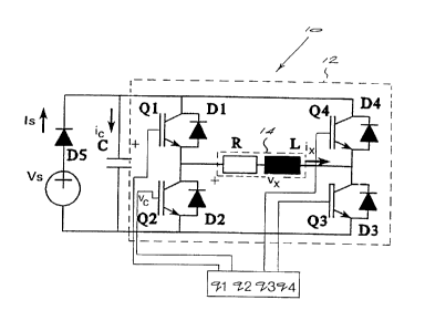
Referring first to Figure 1, a DC to AC converter circuit 10 comprises a full
bridge inverter circuit 12 comprising four switches Q1, Q2, Q3 and Q4
having respective diodes D1, D2, D3 and D4 connected in anti-parallel
across the switches. A coil 14 represented by a resistance R and an
inductance L extends between the left and right switching arms defined by
the switches Q1 and Q2, and Q3 and Q4. A capacitor C is connected in
parallel across the DC voltage source VS and the input of the full bridge
invertor 12. A diode DS is connected directly to the positive side of the
direct voltage source VS, and is arranged to decouple the resonant capacitor
C from the direct voltage source when the voltage across the resonant
capacitor C is in excess of the DC voltage at the voltage source V5.
SUBSTITUTE SHEET (RULE 26)
CA 02271102 1999-OS-06
WO 98I20605 PCT/GB97103081
- 12 -
The switches Ql, Q2, Q3 and Q4 are fully controllable, and are typically
insulated gate bi-polar (IGBT) transistors. Alternatively, the switches are in
the form of bi-polar transistors, MOSFETS, gate turn-off thyristors or any
similar controlled switching devices. The switches are controlled by means
of a control circuit which will be described further on in the specification
with reference to Figures 7 to 10B.
Control of the switches Q 1 to Q4 results in the circuit having three states
for
both positive and negative current in the coil 14. These three states are
illustrated more clearly in Figure 2, which represents one positive switching
cycle. The first state I6 comprises a charging interval during which two
switches, namely Q1 and Q3, are conducting and the diodes D2 and D4 are
reversed biased. During this period, the current amplitude increases. A
subsequent freewheeling interval I 8 occurs when the switch Q 1 and the
diode D4 are conducting, or the switch Q2 and the diode D3 are conducting.
During this period, the current amplitude decreases at a relatively small
rate.
During a discharging interval 20, the diodes D2 and D4 are conducting a
positive coil current, and the switches Q l and Q3 are turned off.
The charging, freewheeling and discharging intervals 16, 18 and 20 together
constitute a single positive switching cycle.
The charging interval 16 is essential to the operation of the inverter as it
then draws power from either the voltage source VS or the resonant capacitor
C. The freewheeling and discharging intervals 18 and 20 provide two
methods for reducing the current, and either or both of these intervals can
be used during circuit operation. This feature of the circuit provides
flexibility not only to control the amplitude or waveform of the output
SUBSTITUTE SHEET (RULE 26)
CA 02271102 1999-OS-06
WO 98/20605 PCT/GB97/03081
- 13 -
current, but also the content and distribution of the frequency spectrum of
the waveform, which is particularly important in the generation of a bipolar
square wave.
The control range extends between two extremes, one in which the decrease
in the coil current is performed solely by the freewheeling interval and the
other in which decrease in coil current takes place solely by the discharging
interval. Current waveforms corresponding to these two modes of operation
are illustrated in Figures 3 and 4.
In the waveform 24 illustrated in Figure 4, the current crest is almost
constant, having a low ripple factor, where the discharging interval is set to
zero. The current waveform has a higher AC ripple factor, when the
freewheeling interval is set to zero, as is illustrated at 25 in Figure 3,
thereby
enhancing the frequency content of the current waveform. Continuous
adjustment of the waveform shapes is possible by adjusting the relative
weighting of the charging, freewheeling and discharging intervals, together
with the number of current pulses in each positive and negative cycle.
The polarity change over intervals 3 and I 1 in Figures 3 and 4~ are initiated
by turning a11 the switches Ql to Q4 off, and providing a discharge path
through the diagonally opposed diodes D2 and D4 or D l and D3. When the
current crosses zero, the switches parallel to the conducting diodes are
closed, thereby taking over the current, which is now travelling in the
opposite direction. This initiates a resonant charging interval that takes the
currents to a value close to the maximum value. This resonant charging
interval involves a resonance between the resonant capacitor C and the coil
inductance L. The peak voltage across the resonant capacitor C is typically
SUBSTITUTE SHEET (RULE 26)
CA 02271102 1999-OS-06
WO 98/20605 PCT/GB97/03081
- 14 -
ten times larger than the supply voltage VS. The following equations
describe the change over transient for coil voltage v~ and coil current iX:
vs(t)=IS 1 a °Z'sin(w2t) +Vs
w2C
(1)
iX(t)=Ise-°~' cos(wzt)- a2 sin(w2t)
wz
(2)
where
2
w2
Lc ( i,
(3)
__R
~2 2L
(4)
and IS is the current peak of the approximate square wave.
Pulse width modulation is applied to control the current amplitude and ripple
SUBSTITUTE SHEET (RULE 26)
CA 02271102 1999-OS-06
WO 98I20605 PCT/GB97/03n81
- 15 - -
on the crest of the positive and negative parts of the square wave during
intervals 2, 4, 10 and 12. Interval 15 is a positive switching cycle
comprising two sub-intervals, namely intervals 13 and 14. Interval 13 is a
charging interval and interval 14 is a freewheeling interval, both intervals
being of the type illustrated at 10 and 12 in Figure 2, which also indicate
which devices are conducting in the circuit. The various numbered intervals
can be summarised as follows:
Intervals l, Current polarity change over
3 :
Intervals 2, Pulse width modulation
4 :
Interval 5 : One pulse width modulation switching
cycle
Interval 6 : Resonant discharging of the coil
Interval 7 . Resonant charging of the coil from
capacitor
Interval 8 : Slow exponential charging of the
coil from
voltage source
Intervals 9, Current polarity change over
11 :
Intervals 10, Pulse width modulation
12 .
Interval 13 Slow exponential charging of the
: coil from
voltage source
Interval 14 Freewheeling (slow exponential discharging)
.
Interval 15 One pulse width modulation positive
: switching
cycle
The waveforms of the slow exponential charging intervals 13 and 8 from the
voltage source are given by the following equations:
SUBSTITUTE SHEET (RU~.E 26)
CA 02271102 1999-OS-06
WO 98/20605 PCT/GB97/03081
- 16 -
Vx(t) = l s
($)
ix(trls)= Vs+ Ix_ Vs B _att
R R
(6)
where Ix is the coil current at the beginning of the interval.
During the freewheeling or slow exponential discharging interval 14 of
Figure 4, almost zero volts is applied to the coil 14. This allows for the
conduction losses of the diode D4 and the switch Q 1, or diode D2 and
switch Q3, depending on which diode/switch pair is operating. The
waveforms during this interval are given by the following equations:
Vx(t) = 0
Ix(t~Ix)=Ixe _att
(8)
where
R
Qi'-
L -
SUBSTITUTE SHEET (RULE 26)
CA 02271102 1999-OS-06
WO 98/20605 PCT/GB97/03081
- 17 -
Interval 5 is a positive current switching cycle, when the freewheeling
interval is reduced to zero using only the resonant discharging interval to
reduce the current during pulse width modulation control. The resonant
discharging interval 6 can be described by the previous resonant charging
equations ( 1 ) and (2).
Intervals 7 and 8 are respective resonant and exponential charging intervals
corresponding to switches Q 1 and Q3 conducting during the positive part of
the cycle, and similarly switches Q2 and Q4 conducting during the negative
part thereof. Interval 8 occurs when the input voltage to the inverter bridge
12 is equal to the supply voltage VS, and equations (5) and (6) describe the
voltage and current waveforms over this period. During interval 7 when the
load 14 is charged from the resonant capacitor C, the impedance R + jwL
of the coil load resonates with the capacitor C, and the waveforms are given
by the following equations:
vX(t,VX,IX)=V +A(Vx,Ix)e ~2'sin(~Zt+~(V,I))
(9)
a
ix(t,Vx,lx)=A(Vx,l ) Cca2e °~' cos(c~2t +~ (Vx,ls)) - w2 sin(c.~Zt
+~(VX,Ix))
2
( 10)
where
SUBSTITUTE SHEET (RULE 26)
CA 02271102 1999-OS-06
WO 98I20605 PCT/GB97/03081
- 18 -
_ -i
~(V , I ) =atan I x + °'2
w2C(Y - YS) w2
(11)
V _v
A(Vs, j ) = x s
sin (~ (Yx ~Ix))
( 12)
with Vr and IT being the initial load voltage and current.
The waveforms shown in Figures 3 to 6 are applicable when a number of
switching intervals exist for each positive and negative half cycle of the
coil
current. These switching intervals provide a means to control the coil
current amplitude. However in cases where the resistance of the coil is large
enough to limit the coil current to a suitable level, or alternatively, when
the
value of the supply voltage is controlled to limit the coil current to a
suitable
level, it is possible to have only one charge and discharge interval per
positive and negative half cycle of the coil current.
Referring now to Figure 5, an analogue control circuit 30 is shown for
providing independent control of the change over interval, as well as
continuous adjustment of the ratio between the charging and freewheeling
intervals. Alternatively and preferably, the control pulses can be generated
by means of a micro-controller. The analogue control circuit 30 comprises
an 8 bit binary counter 32 having a clock input line 34 and output lines 36,
38, 40 and 42 used to realise the waveforms a, b, c and d in Figure 8. The
SUBSTITUTE SHEET (RULE 26)
CA 02271102 1999-OS-06
WO 98I20605
- 19 -
PCT/GB97/03081
counter clock is derived via the clock input line 34 from a PWM clock 42,
which is in turn slaved from a master PWM controller 44. The PWM
controller 44, which is denoted as PWM 1, is also master to two additional
PWM controllers 46 and 48, indicated as PWM2 and PWM3 respectively.
The master-slave arrangement in which the PWM master controller 44
controls the timing of the counter 32 as well as the other slave PWM '
controllers 42, 46 and 48, ensures that a11 the PWM waveforms have the
same frequency and are in phase with one another and with the counter 32.
The width of the PWM pulses at the PWM controllers PWMI, PWM2 and
PWM3 are adjusted by respective pot's 44A, 46A and 48A.
The outputs 36, 38, 40 and 42 are inverted at NOT gates 50, 52, 54 and 56
respectively, with the inverted outputs from the NOT gates 52 and 54
forming the inputs of an AND gate 58. The output of the AND gate 58 in
turn forms the input of a further AND gate 60, which also receives an input
from the NOT gate 50. The output from the AND gate 60 is in turn fed to
the input of an AND gate 62, which also receives an input 64 from the
PWM master controller 44.
Waveforms a and f, which represent the outputs from the respective AND
gates 58 and 60, show how the waveforms a, b and c are used to develop a
pulse sequence of which only one of, eight parts is on and the other seven of
the eight parts are off. The output waveform f is inverted by means of a
NOT gate 66, and the inverted waveform is then passed on as an input to
AND gates 68 and 70. The AND gate 70 has as its other input an output
from an AND gate 72, which in turn receives inputs via input lines 74 and
76 from the PWM controllers PWM2 and PWM3. The PWM2 output line
74 also feeds the AND gate 68 with the output waveforms g, h and i
SUBSTITUTE SHEET (RULE 26)
CA 02271102 1999-OS-06
wo 98no6os
PCT/GB97/03081
- 20 -
representing the outputs from the respective AND gates 62, 68 and 70. The
output waveforms g and h are combined and inverted at a NOT gate 78 so
as to provide a combined inverted output waveform j, which forms an input
of the NAND gates 80 and 82. The output waveform i from the AND gate
70 is inverted so as to provide the output waveform k, which is in turn fed
to inputs of respective NAND gates 88 and 90. The output signals from the
NAND gates 80, 88, 90 and 82 are inverted at respective NOT gates 92, 94,
96 and 98, at which stage they become the PWM control signals indicated
by the waveforms ql, q2, q3 and q4 for switching the respective switches
Q 1, Q2, Q3 and Q4. Each switching cycle can be broken up into sixteen
parts, of which eight parts is always on and the other eight parts is either
always or only partially on, depending on how the pulse width modulators
are set.
The four different pulse sequence switching cycles illustrated at q 1 to q4
are
in respect of a particular example in which the pulse width of PWMZ is
smaller than that of PWM3, as a result of which PWM2 dominates. In
Figure 9A, another example is given of output waveforms rl, r2, r3 and r4
to show what happens when the pulse width of PWM3 is smaller than that
of PWM2.
It is clear from the waveforms q 1 to q4 and r 1 to r4 that there are only two
different pulse sequences, and that q3 and q4 on the one hand and r3 and r4
on the other hand represent the same respective sequences as q 1 and q2, and
rl and r2, but moved 180° out of phase. This is to ensure that the two
switches in each phase arm of the four converters will never be on at the
same time.
SUBSTITUTE SHEET (RULE 26)
CA 02271102 1999-OS-06
WO 98/20605 PCT/GB97/03081
- 21 -
By looking at the final outputs of the control circuit 30, it is clear that by
setting PWM1, the first part of the eight partially on portions of two of the
pulse sequences are set. The other seven parts are set using PWM2. The
other two pulse sequences r 1 and r2 are fully on for the first of each of the
eight on parts and the other seven parts are set by setting PWM2 and
PWM3, with the greater of the two pulse widths dominating (in actual fact,
the smallest pulse width will dominate, but the inverse of the PWM pulses
is being used).
In the circuit, the PWM clock chip 42 controls the number of pulses in
respect of a full cycle of a square wave comprising intervals 1 to 4 in Figure
3 or intervals 9 to 12 in Figure 4. A maximum of 16 pulses per complete
cycle is possible, with 8 pulses per positive and negative half cycle. The
PWM1 controller 44 controls the duration of the transitional polarity change-
over intervals 1 and 3 or 9 and 11. The PWM controllers PWM2 and
PWM3 effectively control the extent of the current "ripple" on the crest
denoted by intervals 2 and 4 in Figure 3 and 10 and 12 in Figure 4. This
is achieved by adjusting the relative length of the charging, freewheeling and
discharging intervals over each switching cycle. By adjusting the relative
lengths of the charging intervals, the magnitude of the waveform may be
varied, as is clear from Figures 3 and 4.
Referring now to Figure 7, a second embodiment of a DC to AC converter
circuit 100 is shown. This is in most respects identical to the circuit of
Figure 1, with the addition of a clamping capacitor C~ shunted across the DC
voltage source Vs in series with a diode D6, which is connected in anti-
parallel with a switch Q5. The provision of the switch Q5, the anti-parallel
diode D6 and the clamping capacitor C~, which effectively operate as a
SUBSTITUTE SHEET (RULE 26)
CA 02271102 1999-OS-06
WO 98/20605 PCT/GB97/03081
- 22 - -
second DC voltage source having a higher DC voltage ( 190V) than the f rst
DC voltage source (70V), allows for two additional modes of operation.
These are a fast exponential charge mode in which the load is charged from
the clamping capacitor via the switch Q5, and a fast exponential discharge
mode in which the load discharges into the clamping capacitor C~ via the
diode D6. The converter circuit 100 controls the current in the magnetic
field coil 14, applying a sequence of the following specific intervals, which
are described in more detail below:
a) A resonant charging interval, which involves a resonance in which
the frequency is substantially smaller than the repetition rate of the
waveform, which occurs between the coil inductance and the
capacitor, and during which the amplitude of the coil current is
increased.
b) A resonant discharging interval, which involves a resonance which
is opposite to that in a), in that the amplitude of the coil current is
decreased.
c) A slow exponential discharge or freewheeling interval, during which
a short circuit is applied across the coil 14, resulting in a slow
exponential decay of the current.
d) A fast exponential discharge interval, during which the clamping
voltage of capacitor C~ is applied across the coil, resulting in a fast
exponential decay of the current arising from the application of a
higher voltage (190V) than the DC input voltage of 70V.
SUBSTtTUTE SHEET (RULE 26)
CA 02271102 1999-OS-06
WO 98I20605 PCT/GB97/03081
- 23 -
e) A slow exponential charging interval during which the supply voltage
is applied to the coil, resulting in a slow exponential rise of the
current.
fJ A fast exponential charging interval during which the clamp voltage
is applied to the coil, resulting in a fast exponential rise of the
current.
g) A quiescent state during which no current flows in the coil and coil
is effectively disconnected.
Figures 7 and 8 illustrate the various current paths in the circuit diagram
and
the states of the diodes and switches corresponding to the various conduction
modes or intervals a) to g) above. These current paths constitute a first set
of sub-circuits making up the main converter circuit in respect of a positive
current cycle. In a negative current cycle, the current direction is reversed
and switches Q2 and Q4 and diodes D 1 and D3 come into operation. The
conduction modes are thus identical to those illustrated in Figures 7 and 8,
save that switches Q1-and Q3 are replaced by respective switches Q2 and
Q4, and diodes D2 and D4 are replaced by respective diodes~Dl and D3,
which make up a second set of sub-circuits operating in identical modes, but
with the diodes and switches carrying current in the opposite direction. In
the freewheel mode, the first freewheel circuit may be constituted either by
current path c), or by a current path constituted by diode D2, coil 14 and
switch Q3. Similarly, the second freewheel current circuit may comprise,
with coil 14, either switch Q4 and diode D 1 or switch Q2 and diode D3.
SUBSTITUTE SHEET (RULE 26)
CA 02271102 1999-OS-06
WO 98I20605 PCT/GB97103081
- 24 -
The current in the coil is cycled between a positive current cycle and a
negative current cycle. During either the positive or -negative cycle the
current is controlled by applying the above intervals in a sequential manner
in order to control the amplitude and the frequency content of the waveform.
The state diagram of Figure 9A indicates all the possible switching
sequences between various modes within a PWM-controlled unipolar
switching cycle. Note that the dead or quiescent interval is not used.
Referring now to Figure 9B, when the current in the coil is changed from
positive to negative or vice versa, in a current polarity transition interval,
can
be achieved by applying a resonant discharge followed by an optional
quiescent state, followed by a resonant charge interval. Alternatively the
polarity can be changed by using a slow exponential discharge interval
followed by an optional quiescent interval, followed by a slow exponential
charge interval. The third option gives the fastest polarity change for a
given voltage stress on the devices and consists of resonant discharge,
followed by a fast exponential discharge, a fast exponential charge and a
resonant charging interval.
The various intervals referred to above will now be described in
mathematical terms. More states and a larger number of interactions
between states are introduced in this second embodiment. Consequently, a
set of equations are presented that are more general and more flexible.
Resonant charging interval:
During the resonant charging interval the coil inductance L is charged by the
resonant capacitor C, and the current is supplied from the capacitor C to the
SUBSTITUTE SHEET (RULE 26)
CA 02271102 1999-OS-06
WO 98/20605 PCT/GB97/03U81
- 25 -
coil L through switches Q l and Q3. Similarly, the negative current is
conducted by switches Q2 and Q4.
The current and voltage waveforms for this interval are given by the
following equations which are essentially similar to but more generalized
than equations (2} and ( 1 ) respectively.
v (0) -Li (0) Q
ix(t)=e-°~ is(0)cos(w2t)+ X LwX 2 sm{w2t}
2
(13)
i (0) -Cv (0) a
v~(t)=e-°2 vs{0)cos(w2t)- x Cwx 2 sln{wet)
2
(14)
where w2 and a2 are defined in equations (3) and (4).
The coil current Ix in this interval increases while the voltage, VX ,
decreases.
Slow exponential charging interval:
This interval also involves conduction of two switches, similar to the
resonant charging interval. Instead of discharging capacitor C, current is
SUBSTITUTE SHEET (RULE 26)
CA 02271102 1999-OS-06
WO 98I20605 PCT/GB97/03081
- 26 -
drawn from the voltage source and DS conducts.
The waveforms for this interval when switches Q 1 and Q3 are conducting,
are given by previous equations (5) and (6).
Fast exponential discharging:
This interval is similar to slow exponential charging interval, and the only
difference is that V~,a",P instead of VS is applied to the coil. QS is
connects
capacitor C~ to the transistor bridge and switches Q 1 and Q3, or Q2 and Q4
are switched on.
The waveforms are described by previous equations (5) and (6), but
replacing VS by V~,a",P.
Slow exponential discharging {freewheeling):
This has already been described with reference to interval 14 of Figure 4 in
equations (7) and (8).
Resonant discharging:
This is given the following equations, which are essentially identical to
equations ( 13 ) and ( 14), save for the change in polarity.
Iz(t)=e-°2 ix(0)cos(w2t)- vx(~)Lwx(o)o2 sm(w2t)
2
SUBSTITUTE SHEET (RULE 26)
CA 02271102 1999-OS-06
WO 98I20605 PCTIGB97/03081
- 27 - _
(15)
vx(t)=-e-°Z s(0)cos(~2t)+ IX(U) Cws(o)a2 sm(~2t)
z
( 16)
As soon as all the switches are turned off the decrease of current proceeds
at an increasing rate, due to an increasing negative voltage that is applied
to
the coil L. For the positive current PWM cycle the current will be
conducted by diodes D2 and D4, whereas for the negative PWM cycle
diodes D l and D3 will be conducting.
As can be seen from equation ( 16), the voltage over the coil L is negative
and this explains the decreasing current indicated by equation (IS).
Fast exponential discharging:
This interval prevents the voltage over the resonant capacitor C from rising
above the value V~,a",p. The inductor to discharge exponentially into the
large capacitor C~.
The wave waveforms for this interval are given by the following equations:
SUBSTITUTE SHEET (RULE 26)
CA 02271102 1999-OS-06
Wb 98/20605 PCT/GB97/03081
- 28 -
vx~t~ ~ lamp
( 17)
Ix(t)= lx(O)+ yclamp e-a~t lamp
R R
(18)
Referring now to Figure 10, which is similar to Figure 3, a coil current
waveform diagram is shown in which the quiescent interval 9 is used during
the current polarity change-over interval 3 so as to provide an optional
variable dead time between positive and negative pulses. The quiescent
interval is preceded by a resonant discharge interval 6, and is followed by
a resonant charge interval 7.
Referring now to Figures 11A to 11C, respective waveform .diagrams of
capacitor current, coil voltage and coil current are shown in respect of the
first embodiment of the converter, in which R = 0.0124S2, C = 12.8mF, and
L = 150mH. The change-over interval 1 comprises a resonant discharge
interval 3 followed by a resonant charge interval 4. A simple P WM interval
2 comprises only a single slow exponential charge interval 5 followed by a
slow exponential discharge interval 6. At the onset of the change-over
interval, the coil current I~ is switched to flow into the capacitor C. The
initial coil voltage VX increases from 70 volts to a maximum of 190 volts as
SUBSTITUTE SHEET (RULE 26)
CA 02271102 1999-OS-06
WO 98/20605 PCT/GB97/0308I
- 29 -
the current amplitude decreases. When the capacitor current reaches zero,
this signals the start of a resonant charge interval in which the amplitude of
the coil and capacitor currents increase and the coil voltage drops back
towards 70 volts. When the current has fully changed polarity, the current
amplitude will be slightly smaller than it was prior to the current change-
over interval due to losses in the circuit. As a result, the unipolar PWM
interval 2 commences with a slow exponential charging interval to restore
the current amplitude, followed by a slow exponential charging interval to
complete a single PWM cycle.
Referring now to Figures 12A to 12D, the current and voltage waveforms
in respect of a clamped circuit of the type illustrated in Figure 7 are shown.
When the coil voltage reaches the clamp voltage level of 190 volts, the
capacitor current stops flowing in the capacitor and commutates to the
clamping circuit during the transition from a resonant discharge interval 3
to a fast exponential discharge interval. When the clamping current flows
the diode D6 conducts and the clamping capacitor absorbs energy from the
coil, resulting in fast exponential discharge interval 7. When the polarity of
the clamping current changes, a switch QS takes over the conduction from
diode D6 and the clamping capacitor discharges back into the coil during the
fast exponential charging interval 8. During this time the current amplitude
increases to almost the same but the opposite value as it was at the onset of
the clamped interval. The effect of the clamping sub-circuit constituted by
the clamping capacitor C~, the switch QS and the anti-parallel diode D6
results in a significant increase in change-over time. In this converter
circuit, the resistance and the inductance remained unchanged, the
capacitance of capacitor C was 4mF, the capacitance of clamping capacitor
was 100mF, and the clamping voltage was 190 volts. The resultant change-
SUBSTITUTE SHEET (RULE 26)
CA 02271102 1999-OS-06
WO 98/20605 PCT/GB97/03081
- 30 -
over interval was reduced from 4.36ms to 2.43ms.
The control circuit supplying gate pulses to QS will typically measure the
current when diode D6 starts to conduct, and will turn off switch QS when
its current reaches the same value, in order to achieve charge balance in
clamping capacitor C~. The value of the clamping voltage on the capacitor
C~ is adjusted by varying the turn-off current of switch Q5, making it either
slightly larger or smaller than the turn-on current of mode D6.
The exceptional versatility of the circuit finds a particular application in
airborne electromagnetic prospecting systems, as it allows for extensive
control of both the amplitude and frequency content of the transmitted
waveform, to the extent that the magnitude of individual frequency
components in the waveform can be controlled so as to achieve the optimum
transmitted magnitude and frequency components of a substantially square
waveform for a particular prospecting application. In particular, higher
frequency components, the magnitude of which are inversely suppressed as
a function of frequency in an ideal square wave, and are even more
suppressed in a quasi-square trapezoidal wave, can be increased where
desired in a controlled manner. Further, the clamping circuit provides for
fast exponential charge and discharge modes of operation which significantly
decrease the bipolar transition interval, thereby increasing the efficiency of
operation and allowing for the transmission of discrete higher frequency
components across a broad frequency spectrum in a wave which approaches
an ideal square wave.
SUBSTITUTE SHEET (RULE 26)