Language selection

Search

Patent 2271142 Summary

Third-party information liability

Some of the information on this Web page has been provided by external sources. The Government of Canada is not responsible for the accuracy, reliability or currency of the information supplied by external sources. Users wishing to rely upon this information should consult directly with the source of the information. Content provided by external sources is not subject to official languages, privacy and accessibility requirements.

Claims and Abstract availability

Any discrepancies in the text and image of the Claims and Abstract are due to differing posting times. Text of the Claims and Abstract are posted:

  • At the time the application is open to public inspection;
  • At the time of issue of the patent (grant).
(12) Patent: (11) CA 2271142
(54) English Title: SYSTEM AND METHOD FOR ATM CBR TIMING RECOVERY
(54) French Title: SYSTEME ET PROCEDE SERVANT A RECUPERER LA SYNCHRONISATION DU DEBIT BINAIRE CONSTANT EN MODE DE TRANSFERT ASYNCHRONE
Status: Deemed expired
Bibliographic Data
(51) International Patent Classification (IPC):
  • H04J 3/06 (2006.01)
(72) Inventors :
  • BERNSTEIN, GREG M. (United States of America)
(73) Owners :
  • NORTEL NETWORKS LIMITED (Canada)
(71) Applicants :
  • NORTHERN TELECOM LIMITED (Canada)
(74) Agent: SMART & BIGGAR
(74) Associate agent:
(45) Issued: 2002-04-16
(86) PCT Filing Date: 1997-11-07
(87) Open to Public Inspection: 1998-05-14
Examination requested: 1999-11-05
Availability of licence: N/A
(25) Language of filing: English

Patent Cooperation Treaty (PCT): Yes
(86) PCT Filing Number: PCT/IB1997/001408
(87) International Publication Number: WO1998/020637
(85) National Entry: 1999-05-06

(30) Application Priority Data:
Application No. Country/Territory Date
08/746,176 United States of America 1996-11-07

Abstracts

English Abstract


A system in a receiver of ATM cells determines an average cell interarrival
time by determining the amount of time required for a predetermined number of
cells to arrive. The system then uses the average cell interarrival time to
adjust the internal timing of the receiver.


French Abstract

Système dans un récepteur de cellules de mode de transfert asynchrone (ATM) déterminant un temps moyen d'arrivée de cellules au moyen du calcul du temps nécessaire à l'arrivée d'un nombre prédéterminé de cellules. Ce système utilise ensuite ce temps moyen d'arrivée afin de régler la synchronisation interne du récepteur.

Claims

Note: Claims are shown in the official language in which they were submitted.


-8-
Claims

1. A method of recovering the timing from an asynchronous stream composed of
cells transmitted at a relatively constant bit rate comprising the steps of:
detecting, at a receiver, the receipt of a predetermined number of cells;
measuring the internal receiver time elapsed during the receipt of the
predetermined number of cells, the internal receiver time being derived from a
timing source in the receiver; and
adjusting the timing source according to the measured internal receiver
time.
2. The method of claim 1 further including the step of
determining an average cell interarrival time for the detected cells from
the measured internal receiver time; and
wherein step of adjusting the system timing includes the substep of
adjusting the system timing according to the average cell interarrival time.
3. The method of claim 2 wherein the step of determining an average cell
interarrival time includes the substeps of
- detecting the arrival of a new cell, and
incrementing a cell count upon the detection of the arrival of a new cell.
4. The method of claim 3 wherein the substep of incrementing a cell count
includes
the substep of
generating a count signal when the cell count reaches a predetermined
amount; and
wherein the step of measuring the internal receiver time includes the substep
of
receiving the count signal, and
recording the internal receiver time elapsed when the count signal is
received.
5. A method of recovering the timing of an Asynchronous Transfer Mode (ATM)
stream composed of ATM cells comprising the steps of:
detecting, at a receiver, the receipt of a predetermined number of proper
ATM cells;
measuring the internal receiver time elapsed during the receipt of the


-9-

predetermined number of ATM cells, the internal receiver time being derived
from
a timing source in the receiver; and
adjusting the timing source according to the measured internal receiver
time.
6. The method of claim 5 further including the step of
determining an average cell interarrival time for the detected ATM cells
from the measured internal receiver time; and
wherein step of adjusting the system timing includes the substep of
adjusting the system timing according to the average cell interarrival time.
7. The method of claim 5 wherein the step of detecting the receipt of a
predetermined number cells includes the substeps of
extracting a VPI/VCI value from a current one of the ATM cells;
examining the extracted VPI/VCI value to determine whether the current
ATM cell is a proper ATM cell.
8. The method of claim 7 wherein the substep of examining the VPI/VCI includes
the
substeps of
storing into a VPI/VCI register a value corresponding to a desired type of
cell, and
incrementing a cell count when the contents of the extracted VPI/VCI
register equal the VPI/VCI values.
9. The method of claim 8 wherein the substep of incrementing a cell count
includes
the substep of
generating a count signal when the cell count reaches a predetermined
amount; and
wherein the step of measuring the internal receiver time includes the substeps
of
receiving the count signal, and
recording the internal receiver time elapsed when the count signal is
received.
10. A method of sending an asynchronous stream composed of cells comprising
the
steps of:
transmitting the stream at a relatively constant bit rate;
receiving the stream at a receiver;


-10-

detecting, at the receiver, the receipt of a predetermined number of cells;
measuring the internal receiver time elapsed during the receipt of the
predetermined number of cells, the internal receiver time being derived from a
timing source in the receiver; and
adjusting the timing source according to the measured internal receiver
time.
11. The method of claim 10 further including the step of
determining an average cell interarrival time for the detected cells from
the measured internal receiver time; and
wherein step of adjusting the system timing includes the substep of
adjusting the system timing according to the average cell interarrival time.
12. The method of claim 11 wherein the step of determining an average cell
interarrival time includes the substeps of
detecting the arrival of a new cell, and
incrementing a cell count upon the detection of the arrival of a new cell.
13. The method of claim 12 wherein the substep of incrementing a cell count
includes
the substep of
generating a count signal when the cell count reaches a predetermined
amount; and
wherein the step of measuring the internal receiver time includes the substep
of
receiving the count signal, and
recording the internal receiver time elapsed when the count signal is
received.
14. A method of sending an Asynchronous Transfer Mode (ATM) stream composed
of ATM cells comprising the steps of:
transmitting the message at a relatively constant bit rate;
receiving the message at a receiver;
detecting, at the receiver, the receipt of a predetermined number of proper
ATM cells;
measuring the internal receiver time elapsed during the receipt of the
predetermined number of ATM cells, the internal receiver time being derived
from a timing source in the receiver; and


-11-

adjusting the timing source according to the measured internal receiver
time.
15. The method of claim 14 further including the step of
determining an average cell interarrival time for the detected ATM cells
from the measured internal receiver time; and
wherein step of adjusting the system timing includes the substep of
adjusting the system timing according to the average cell interarrival time.
16. The method of claim 14 wherein the step of detecting the receipt of a
predetermined number cells includes the substeps of
extracting a VPI/VCI value from a current one of the ATM cells;
examining the extracted VPI/VCI value to determine whether the current
ATM cell is a proper ATM cell.
17. The method of claim 16 wherein the substep of examining the VPI/VCI
includes
the substeps of
storing into a VPI/VCI register a value corresponding to a desired type of
cell;
incrementing a cell count when the contents of the VPI/VCI register equal
the extracted VPI/VCI values.
18. The method of claim 17 wherein the substep of incrementing a cell count
includes
the substep of
generating a count signal when the cell count reaches a predetermined
amount; and
wherein the step of measuring the internal receiver time includes the
substeps of
receiving the count signal, and
recording the internal receiver time elapsed when the count signal is
received
19. A system in a receiver to recover the timing of a stream composed of cells
sent at
a relatively constant bit rate comprising:
monitor means for detecting the receipt of a predetermined number of
cells;
an internal receiver clock recording internal receiver time;


-12-

timer means for measuring the internal receiver time elapsed during the
receipt of the predetermined number of cells; and
correction means for adjusting the internal receiver clock according to the
measured internal receiver time.
20. The system of claim 19 wherein the internal receiver clock is a voltage-
controlled
oscillator, and
wherein the correction means includes
a digital-to-analog converter generating a feedback voltage signal for the
voltage-controlled oscillator.
21. The system of claim 20 wherein the internal receiver clock includes
a clock signal divider, coupled to an output of the voltage-controlled
oscillator, to generate pulses at a lower frequency than the voltage-
controlled
oscillator, and wherein the timer means includes
a counter to count the pulses generated by the clock signal divider.
22. The system of claim 20 wherein the correction means includes
means for determining an average cell interarrival time for the detected
cells from the measured internal receiver times, and
means for adjusting the internal receiver clock according to the average
cell interarrival time.
23. A system in a receiver to recover the timing of a stream composed of cells
sent at
a relatively constant bit rate comprising:
monitor means for detecting the receipt of a predetermined number of
ATM cells;
an internal receiver clock recording internal receiver time;
timer means for measuring the internal receiver time elapsed during the
receipt of the predetermined number of ATM cells; and
correction means for adjusting the internal receiver clock according to the
measured internal receiver time.
24. The system of claim 23 wherein the internal receiver clock is a voltage-
controlled
oscillator, and
wherein the correction means includes


-13-

a digital-to-analog converter generating a feedback voltage signal for the
voltage-controlled oscillator.
25. The system of claim 24 wherein the internal receiver clock includes
a clock signal divider, coupled to an output of the voltage-controlled
oscillator, to generate pulses at a lower frequency than the voltage-
controlled
oscillator; and wherein the timer means includes
a counter to count the pulses generated by the clock signal divider.
26. The system of claim 24 wherein the correction means includes
means for determining an average cell interarrival time for the detected
ATM cells from the measured internal receiver time; and
means for adjusting the internal receiver clock according to the average
cell interarrival time.
27. The system of claim 23 wherein the monitor means includes
a network extraction circuit for extracting from the cells data
corresponding to the ATM layer;
a VPI/VCI extraction register, coupled to the network extraction circuit,
for storing current VPI/VCI value in the cells; and
a comparator, coupled to the VPI/VCI extraction register, for examining
the current VPI/VCI values to determine the receipt of a proper ATM cell.
28. The system of claim 27 wherein the monitor means further includes
a VPI/VCI matching register, coupled to the comparatar circuit and
containing the values of the cell header predetermined to be proper.
29. The system of claim 28 wherein the comparator includes
means for generating a cell signal indicating the receipt of a proper new
cell; and
wherein the monitor means further includes
a cell counter, coupled to receive the cell signal from the comparator,
configured to increment a cell count upon receipt of the cell signal and
generate a
count signal when the cell count reaches a predetermined amount.
30. The system of claim 29 wherein the means for measuring the internal
receiver time
elapsed during the receipt of the predetermined number of ATM cells includes


-14-

a counter to count the internal receiver time and stop upon receipt of a
count signal.
31. A receiver receiving a plurality of cells intended to be transmitted at a
constant bit
rate, the receiver comprising:
a receiving section to buffer the contents of the cells;
a processing section, coupled to the receiving section, to process the cells;
and
a timing section to generate an internal timing signal for the receiving
section and the processing section, the timing section including
means for detecting the receipt of a predetermined number of cells;
an internal receiver clock generating the internal timing signal;
means, coupled to the internal timing signal for measuring the
internal receiver time elapsed during the receipt of the predetermined
number of cells; and
correction means for adjusting the internal receiver clock according
to the measured internal receiver time.
32. A receiver receiving a plurality of ATM cells intended to be transmitted
at a
constant bit rate, the receiver comprising:
a receiving section to buffer the contents of the ATM cells;
a processing section, coupled to the receiving section, to process the ATM
cells; and
a timing section to generate an internal timing signal for the receiving
section and the processing section, the timing section including
means for detecting the receipt of a predetermined number of ATM
cells;
an internal receiver clock generating the internal timing signal;
means, coupled to the internal timing signal for measuring the
internal receiver time elapsed during the receipt of the predetermined
number of ATM cells; and
monitor means for adjusting the internal receiver clock according to the
measured internal receiver time.
33. A system for transmitting a plurality of cells comprising:


-15-

a transmitter sending the cells at a relatively constant bit rate; and
a receiver, receiving the cells and including
a receiving section to buffer the contents of the cells,
a processing section, coupled to the receiving section, to process the cells,
and
a timing section to generate an internal timing signal for the receiving
section and the processing section, the timing section including
means for detecting the receipt of a predetermined number of cells;
an internal receiver clock generating the internal timing signal;
means, coupled to the internal timing signal for measuring the
internal receiver time elapsed during the receipt of the predetermined
number of cells; and
monitor means for adjusting the internal receiver clock according
to the measured internal receiver time.
34. A system for transmitting a plurality of ATM cells comprising:
a transmitter sending the ATM cells at a relatively constant bit rate; and
a receiver, receiving the ATM cells and including
a receiving section to buffer the contents of the ATM cells,
a processing section, coupled to the receiving section, to process the ATM
cells, and
a timing section to generate an internal timing signal for the receiving
section and the processing section, the timing section including
means for detecting the receipt of a predetermined number of ATM
cells;
an internal receiver clock generating the internal timing signal;
means, coupled to the internal timing signal for measuring the
internal receiver time elapsed during the receipt of the predetermined
number of ATM cells; and
monitor means for adjusting the internal receiver clock according
to the measured internal receiver time.

Description

Note: Descriptions are shown in the official language in which they were submitted.


CA 02271142 1999-OS-06
WO 98/20637 PCTlIB97/01408
-I-
SYSTEM AND METHOD FOR ATM CBR TIMING RECOVERY
Back~rg na a Art
The present invention relates in general to the field of packet switching
networks,
and in particular to the field of recovering timing across a packet switching
network, such
as an Asynchronous Transfer Mode (ATM) network, that transmits fixed length
packets
or cells.
Certain services to be carried on packet switching network require
synchronization between the transmitting source and receiver at a layer in the
OSI model
above the physical layer, typically the transport or application layers.
Examples of these
services include voice and video. Some of the services use constant bit rate
(CBR)
streams carried over a packet switched network. These CBR streams are
sequences of
packets that contain data generated by a source at a constant bit rate.
The need to recover timing for CBR streams exists to prevent data buffer
underflow or overflow in the receiver and thus a loss of data. This
synchronization is at a
higher layer than the segment-by-segment physical layer timing recovery
required of any
link in either a packet or circuit switched network.
One technique for recover timing uses a synchronous residue time stamp (SRTS)
which United States Patent Nos. 5,260,978 and 4,9b1,188 describe. The SRTS
technique, however, cannot be used unless there is end-to-end physical layer
timing
synchronization between the source and destination. Many ATM LAN switches do
not
permit this type of timing distribution, in addition some types of links such
as DS-3
carrying ATM also preclude it. ,
Other techniques seek to derive timing from the packet or ATM layer itself
based
upon the CBR nature of the packet or cell stream. United States Patent Nos.
5,396,492
and 5,287,182 use the fill level of a First InlFirst Out (FIFO) buffer at the
receiver to
indicate whether the recovered clock at the receiving end is too fast or too
slow. If the
FIFO buffer fill level increases, the receiver clock is too slow; if the FIFO
buffer fill level
decreases, the receiver clock is too fast.
CONFIRMATION COPY


CA 02271142 1999-OS-06
WO 98I20637 PCT/IB97/01408
-2-
Unfortunately, these techniques suffer major drawbacks. For example, lost
cells
cause the FIFO fill level to indicate a fast clock even if the clock is
synchronized. Also
the fill level technique requires several cells to be buffered in order to
operate properly,
and the time needed to receive all these cells can be large enough to affect
the critical
delay requirement for some applications, such as PBX like voice networks.
Third, buffer
overflow or underflow will also adversely affect the operation of such a
system, such as
results in under or over reporting of clock rate correction.
There is, therefore, a need for a system that recovers timing from CBR cell
transmissions without adversely affecting receiver operation or using SRTS
techniques.
Such a system should, in addition, not be affected by buffer overflows or
underflows in a
receiver circuit.
Disclosure of the Invention
This invention meets those needs by determining the time required to receive a
predetermined number of cells. That time can be converted into an average cell
interarrival time that can in turn be used to control the receiver's internal
timing system.
In particular, a method consistent with this invention of recovering the
timing of a
CBR packet stream, such as an Asynchronous Transfer Mode (ATM) CBR virtual
channel (VC), includes the steps of. detecting, at a receiver, the receipt of
a
predetermined number of cells (or packets); measuring the internal receiver
time elapsed
during the receipt of the predetermined number of cells (or packets), the
internal receiver
time being derived from a timing source in the receiver; and adjusting the
timing source
according to the measured internal receiver time.
A system consistent with this invention to recover the timing of a CBR packet
stream, such as an Asynchronous Transfer mode (ATM) CBR virtual channel (VC),
includes means for detecting the receipt of a predetermined number of cells;
an internal
receiver clock recording internal receiver time; means for measuring the
internal receiver
time elapsed during the receipt of the predetermined number of cells; and
means for
adjusting the internal receiver clock according to the measured internal
receiver time.
Brief Description of the Drawings
The accompanying drawings, which are incorporated in and constitute a part of
this specification, illustrate embodiments of the invention and, together with
the


CA 02271142 1999-OS-06
WO 98/20637 PCT/IB97/01408
-3-
description, explain the objects, advantages, and principles of the invention.
In the
drawings:
Figure I is a representation of an ATM cell;
Figure 2 is a functional block diagram of a technique of recovering timing
from a
CBR cell stream consistent with this invention;
Figure 3 is a block diagram of a receiver system that uses this invention;
Figure 4 is a diagram of the timing section in the receiver system of Figure
3;
Figure 5 is a flowchart of the steps performed by the control circuit in the
timing
section of Figure 4;
Figure 6 is a frequency vs. time a graph from a simulation of timing recovery
method consistent with this invention; and
Figure 7 is a frequency vs. time a graph from another simulation of timing
recovery method consistent with this invention.
Best Mode for Carrying Out the Invention
Reference will now be made to preferred implementations of this invention,
examples of which are shown in the accompanying drawings. In those drawings,
like
reference numbers in different drawings refer to the same elements.
The present invention is described with regard to an ATM system, although it
need not be limited to such a system. ATM systems transmit 53-byte cells.
Figure 1
shows a diagram of an ATM cell 100 with an five-byte of header and a forty-
eight-byte
"payload." ATM switches create virtual channels (VCs) to route each cell to
its
destination, and the header for each cell in the same VC includes a VCI/VPI
field
identifying the VC. The VPI/VCI field thus allows the preferred implementation
of this
invention to look only at cells from only one data stream (VC) when
controlling a clock
for the ATM receiver.
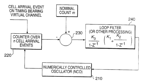
Figure 2 is a functional block diagram demonstrating a technique according to
the
present invention for recovering timing from a CBR stream. Essentially, the
invention
involves correcting the receiver's clock according to an average cell
interarrival time.
That time may be derived from the time required to receive a predetermined
number of
cells.


CA 02271142 1999-OS-06
WO 98/Z0637 PCT/IB97/01408
-4-
In Figure 2, numerically controlled oscillator (NCO) 210, preferably a high-
frequency oscillator, drives a counter 220 to measure the interarrival time
between n
successive cells from a CBR message. The nominal frequency of NCO 2l0, fNCO,
is
(fin)*.fso~«~+ (error),
where m is a scaling value and f o,~~~ is the transmission frequency of the
cells.
After n cells arrive on a selected VC, adder 230 subtracts the contents of
counter
220 from m to accomplish one level of scaling. Processing circuitry 240 then
determines
an average cell interarrival time and performs any necessary filtering,
scaling and other
processing to create the proper signal to correct the value of NCO 210.
This invention can be used in an ATM transmission system, such as system 300
in
Figure 3. In system 300, transmitter 310 sends CBR cells to receiver 320.
Receiver 320
includes a timing section 330 to generate an internal timing signal t~, a
receiving section
340 to extract the contents of the cells and buffer them, and a processing
section 3 SO to
perform necessary processing, such as error correction, on the cells.
Figure 4 is a more detailed block diagram of portions of extraction section
340
and timing section 330. In extraction section 330, PHY and ATM layer circuitry
40S
extracts from the input ATM stream an SOC (start of cell) signal and the data
bytes from
the cells. PHY and ATM layer circuitry 40S sends the SOC signal to control
circuitry 310
and sends the data bytes to the rest of receiver 320 on a bus operating under
the UTOPIA
standard.
In timing section 330, VPI/VCI extraction register 41 S examines header
information from the data bytes. In response to control circuitry 410,
register 41 S
extracts the VPI/VCI values for the current ATM cell.
Comparator 420 compares those extracted values to VPI/VCI values
microprocessor 430 stored in VPI/VCI matching register 42S. In the preferred
embodiment, microprocessor 430 stores in register 42S a predetermined VPI/VCI
value
for a virtual channel carrying a CBR stream. Focusing on cells from only one
VC and
examining the header filters out, among other things, OA&M (operation,
administration,
and maintenance) cells that should not be used to correct timing.
When comparator 420 determines that the VPI/VCI values from these two
registers match, it sends a count signal to cell counter 43 S and through that
counter to
control circuitry 410. Cell counter 43 S keeps track of the number of cells
received.


CA 02271142 1999-OS-06
WO 98/20637 PCT/IB97/01408
_S_
When cell counter 43S reaches a preset value, represented in Figure 4 as N,
counter 43S
sends a completion signal to control circuit 410.
During this operation, VCO 440 generates the receiver system clock according
to
a voltage generated by digital-to-analog converter (DAC) 44S. Together, VCO
440 and
DAC 44S form an NCO.
A divider circuit 4S0 divides the system clock by a constant, shown as p, to
reduce
VCO 440's frequency to a nominal (m/n)*fso,~~~. Interarrival Time Counter 4SS
counts the
output of divider circuit 4S0 to measure interarrival times.
When control circuit 410 receives the completion signal from counter 43 S, it
signals counter 4SS to transfer to buffer 460 its count of the number of VCO
440 clock
pulses (divided by p) between N cell arrivals on the VC indicated by the value
in VPI/VCI
matching register 42S. Control circuit 410 then resets counters 435 and 4S5
and sends an
interrupt to microprocessor 430.
In response, microprocessor 430 reads buffer register 4b0 and implements loop
filtering and any nonlinear processing necessary to ensure a smooth operation
by
eliminating sudden or singular changes The result of the processing is a new
value that
microprocessor 430 sends to DAC 44S to set VCO 440's frequency.
To prevent error from lost cells, control circuit 410 can also direct VPI/VCI
extraction circuit 41 S to extract from a cell's header the sequence number in
the ATM
adaptation layer if used. Then, either control circuit 410 or microprocessor
430 can
determine whether each cell is received in the proper sequence. If cells are
lost, they
would not be in the proper sequence and the results of the processing on that
cell should
not be used to adjust the VCO.
Control circuit 410, which can be a programmable processor, dedicated
circuitry,
a state machine, or any other equivalent structure, performs several functions
represented
by the flowchart S00 in Figure S. Upon receiving a reset signal from the
microprocessor
430, control circuit 410 resets cell counter 43 S and Interarrival Time
Counter 45 S (step
S 10). Then, on receipt of the SOC signal from the PHY and ATM level circuitry
40S,
control circuit 410 latches the VPI/VCI fields from the ATM cell header into
VPI/VCI
extraction register 41 S (step 520). When the VPI/VCI values in registers 41 S
and 42S
first match, control circuitry 410 enables Interarrival Time Counter 455, but
cell counter
43 S does not begin to count. Cell counter 43 S increments with each
additional VPI/VCI


CA 02271142 1999-OS-06
WO 98/20637 PCT/IB97101408
-6-
match until counter 43 5 reaches N. This operation ensures that cell counter
43 5 reaches
N after receiving N interarrival times.
At that point control circuit 410 latches the value of Interarrival Time
Counter
4S5 into buffer 460 (step 530), asynchronously resets Interarrival Time
Counter 455 and
cell counter 435, and interrupts microprocessor 430 to let it know a value is
available in
buffer 460 (step 540).
Both Interarrival Time Counter 455 and cell counter 435 are enabled for
counting
immediately following reset. Also, for ongoing operation, steps 520 - 540
repeat.
Figures 6 and 7 show graphs of frequency vs. time for simulations of a timing
recovery method according to this invention. The loop parameters for the
simulation
represented by Figure 6 were set for very fast frequency capture in a
noiseless (i.e., no cell
delay variation or CDV) environment, and shows the loop rapidly pulling in the
frequency
from a -1000Hz frequency offset. The simulation represented by Figure 7 shows
the loop ---
with somewhat relaxed parameters, pulling in from a -IOOOHz frequency offset
in the
presence of noise (i.e., CDV).
This invention has several advantages over conventional methods that rely on
buffer level fill. For example, buffer underflows or overflows do not affect
the clock
recovery mechanism. Also, unlike the buffer fill level, cell interarrival time
is directly
related to the transmission frequency. For low CDV, this invention's inherent
higher
accuracy permits faster timing acquisition.
There are other advantages as well. For example, as explained above, cell loss
can
drive a FIFO fill-level-based method off track due to a constantly lower cell
fill level. The
present invention can easily compensate for the effects of lost cells. In
addition, FIFO fill-
level-based circuits must buffer a number of cells to operate accurately, but
the time
required for such causes extra delays. The present invention does not suffer
that
disadvantage.
Persons of ordinary skill will appreciate how to make modifications and
variations
to the preferred implementation without departing from the spirit and scope of
the
invention. For example, the transmission system does not need to be an ATM
system,
and the digital circuitry in Figure 3 can be implemented in ASICs, PALS, or
programmable logic devices. Also, for certain networks, signals other than the
VPI/VCI
values can be used.


CA 02271142 1999-OS-06
WO 98/20637 PCT/IB97/01a08
_ '7
This description is intended for proposed illustration and description, and
does not
contain an exhaustive description of embodiments or limit the invention to the
precise
farm disclosed. One of ordinary skill may modify and vary the invention in
light of the
above teachings. The scope of the invention is defined by the appended claims
and their
equivalents.

Representative Drawing
A single figure which represents the drawing illustrating the invention.
Administrative Status

For a clearer understanding of the status of the application/patent presented on this page, the site Disclaimer , as well as the definitions for Patent , Administrative Status , Maintenance Fee  and Payment History  should be consulted.

Administrative Status

Title Date
Forecasted Issue Date 2002-04-16
(86) PCT Filing Date 1997-11-07
(87) PCT Publication Date 1998-05-14
(85) National Entry 1999-05-06
Examination Requested 1999-11-05
(45) Issued 2002-04-16
Deemed Expired 2005-11-07

Abandonment History

There is no abandonment history.

Payment History

Fee Type Anniversary Year Due Date Amount Paid Paid Date
Registration of a document - section 124 $100.00 1999-05-06
Application Fee $300.00 1999-05-06
Maintenance Fee - Application - New Act 2 1999-11-08 $100.00 1999-10-21
Request for Examination $400.00 1999-11-05
Registration of a document - section 124 $0.00 2000-02-07
Maintenance Fee - Application - New Act 3 2000-11-07 $100.00 2000-10-23
Maintenance Fee - Application - New Act 4 2001-11-07 $100.00 2001-10-23
Final Fee $300.00 2002-01-25
Registration of a document - section 124 $0.00 2002-10-30
Maintenance Fee - Patent - New Act 5 2002-11-07 $350.00 2003-03-20
Maintenance Fee - Patent - New Act 6 2003-11-07 $150.00 2003-10-22
Owners on Record

Note: Records showing the ownership history in alphabetical order.

Current Owners on Record
NORTEL NETWORKS LIMITED
Past Owners on Record
BERNSTEIN, GREG M.
NORTEL NETWORKS CORPORATION
NORTHERN TELECOM LIMITED
Past Owners that do not appear in the "Owners on Record" listing will appear in other documentation within the application.
Documents

To view selected files, please enter reCAPTCHA code :


To view images, click a link in the Document Description column. To download the documents, select one or more checkboxes in the first column and then click the "Download Selected in PDF format (Zip Archive)" or the "Download Selected as Single PDF" button.

List of published and non-published patent-specific documents on the CPD .

If you have any difficulty accessing content, you can call the Client Service Centre at 1-866-997-1936 or send them an e-mail at CIPO Client Service Centre.


Document
Description 
Date
(yyyy-mm-dd) 
Number of pages   Size of Image (KB) 
Cover Page 1999-07-27 1 36
Representative Drawing 2002-03-12 1 10
Representative Drawing 1999-07-27 1 10
Cover Page 2002-03-12 1 36
Abstract 1999-05-06 1 39
Description 1999-05-06 7 331
Claims 1999-05-06 8 331
Drawings 1999-05-06 6 89
Assignment 2000-09-25 29 1,255
Assignment 2000-01-06 43 4,789
Correspondence 2000-12-01 2 55
Fees 2003-03-20 2 85
Assignment 1999-05-06 3 127
PCT 1999-05-06 10 328
Prosecution-Amendment 1999-11-05 1 44
Correspondence 2000-02-08 1 45
Correspondence 2002-01-25 1 41
Correspondence 2005-01-04 2 187