Note: Descriptions are shown in the official language in which they were submitted.
GR 97 P 3249
Description
Screened mounting rack for electrical printed circuit
board assemblies.
In terms of its basic structure, a mounting rack
for electrical printed circuit boards quite generally
contains two side wall plates 'which are connected to one
another by transverse rails. I:n this case, the front and
rear sides of the mounting rack: are each formed by a pair
of upper and lower transverse rails. Opposite pairs of
guide rails are latched into these transverse rails . in
order to form so-called insertion slots. The printed
circuit boards, also calledl printed circuit board
assemblies, can be pushed into these vertically standing
parallel next to one another.
Printed circuit boards quite generally have a so-
called front panel, which covers the printed circuit
board on a front side and serves as a holding surface for
a wide variety of display, operating and contact
elements. The front panels of printed circuit boards
pushed into a mounting rack vertically next to one
another then form a virtually closed surface that covers
the front side of the mounting rack.
For the purpose of electromagnetic screening, the
front panels of printed circuit boards are, on the one
hand, produced from an electrically conductive material
or are at least coated by such a material.
DE 36 04 860 C2 and US 4,63l,641 disclose
arrangements for the radiofrequency-proof screening of
front panels situated vertically next to one another on
the front side of a mounting rack. In these cases, the
front panels are electrically conductively interconnected
via vertical contact spring eatrips, his enables the
vertical grooves on the front side of a mounting rack to
be sealed against the entry or the radiation of electro
magnetic interference
A problem with this electromagnetic sealing
arises at the lower and upper narrow sides of each front
CA 02271151 1999-OS-07
GR 97 P 3249 - 2 -
panel. At these locations, mounting screws by means of
which the front panels can be screwed to e.g. threaded-
hole rails, which are pushed into transversely running
accommodating grooves on the front sides of the lower and
upper transverse rails of the mounting rack, are
admittedly present as a general rule. By means of these
mounting screws, it is possible to establish an
electrically conductive connection between the ends of
each front panel and the frame: of the mounting rack via
transverse rails thereof. Howe~;rer, these connections are
only at points and do not extend over the entire width of
the respective front panel. Particularly in the case of
wide front panels of printed circuit board assemblies
which occupy the volume of more than one standard
insertion slot in the interior of the mounting rack, such
an electrically conductive cor.~nection at points between
the front panel and the mounting rack's transverse rails
running behind it at its ends ;is inadequate for reliable
electromagnetic screening.
The same problem also arises with covering plates
e.g. on the rear side of mounting racks. These are also,
as a rule, connected only at points via screws to the
transverse rails running on the upper side and underside
of the rear side of the mounting rack.
Moreover, DE 195 23 257 Cl, which is not a prior
publication, discloses a mounting rack in which the
metallic or metallized front panels of the assemblies are
conductively connected via leaf springs to the front
profiled rails. In this case, one leaf spring has a
fixing part which is fastened to a limb of the profile
rail which forms a groove. The leaf spring itself has
resilient parts by means of which the electrical contact
with the front panel and the profiled rail in the pushed-
in state is established.
DE 296 18 625 U1 dis~~loses~a further screened
mounting rack. Its module rails each have an upper and a
lower engagement groove behind their bearing surfaces.
Contact spring strips which can be snapped onto the
bearing surfaces are provided, which contact spring
CA 02271151 1999-05-07
GR 97 P 3249 - 3 -
strips latch elastically into the engagement grooves by
engaging behind the bearing surfaces. The contact spring
strips have a number of knockouts pointing resiliently to
the front side of the mounting rack and also a number of
contact claws pointing to the bearing surface.
In the case of the contact spring strips of the
known screened mounting racks, wear-induced damage may,
possibly, not be completely avoidable particularly. when
pressure forces stemming not just from the bearing of
front panels are exerted on the contact springs of the
spring strips. Particularly when gripping levers are
fitted to the longitudinal ends of the front panels of
assemblies, by means of which l~rs .the associated a
assembly can at least be levered out of the mounting
rack, considerable bending forces may be exerted at
points on the contact spring strips.
The invention is based on the object of
developing a mounting rack in such a way that the
electromagnetic contact-making of areal elements such as,
in particular, front panels of pushed-in printed circuit
board assemblies and rear covering plates with the lower
and upper transverse rails on t:he front and/or rear side
of the mounting rack is ensured even when the contact
spring strips used are not always loaded only over the
whole area by pressure forces exerted via the inner
surfaces of front panels.
The object is achieved by means of the mounting
rack specified in Claim 1. Further, advantageous embodi-
ments of the invention are specified in the subclaims.
The invention is explained in more detail using
exemplary embodiments illustrated in the figures referred
to briefly below, in which:
FIG. 1 . shows a sectional illustration through an
exemplary mounting rack with a first design of
a front element for a printed circuit board
assembly and with electromagnetic screening,
configured according to the invention, of the
ends of the front element in the region of the
transverse rails,
CA 02271151 1999-OS-07
GR 97 P 3249 - 4 -
FIG. 2 . shows a plan view of the exemplary front
element according to the design of Figure 1,
FIG. 3 . shows a side view of a second design of a
printed circuit board assembly front element
which can be used in the mounting rack
according to the invention,
FIG. 4 . shows a sectional illustration through a
preferred design oj: a contact spring strip
according to the invention,
FIG. 5 shows a sectional illustration through a
mounting rack according to the invention in the
region of the lower transverse rail,
FIG. 6 . shows a perspectiv~_ plan view of the lower
transverse rail of a mounting rack according
to
the invention, in accordance With the design
of
Figure 5, and
FIG. 7 . shows a perspective plan view of a detail of
the preferred embodiment for a contact spring
strip according to the invention as shown in
Figure 7,
FIG. 8a . shows a side view of a mounting rack in the
region of the lower transverse rail, a gripping
lever being fitted to the lower end of the
front element, and the associated assembly
being pushed completely into the mounting rack,
FIG. 8b . shows a side view corresponding to the illus-
tration of Fig. 8a, the associated electrical
printed circuit board assemblies having already
been levered at least partially out of the
mounting rack by actuation of the gripping
lever,
FIG. 8c . shows a side view corresponding to the illus-
tration of Fige 8a, 8b the associated electri
cal circuit board assemblies having been
levered completely out of the mounting rack by
actuation of the gripping lever.
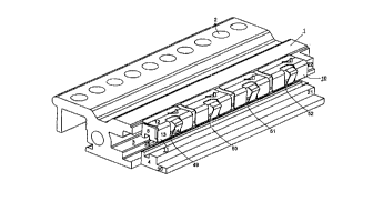
Figure 1 shows a sectional illustration through
an exemplary mounting rack :in the region of its front
side 20, which serves for retaining electrical printed
CA 02271151 1999-OS-07
GR 97 P 3249 ~ - 5 -
circuit board assemblies which. can be pushed in verti
cally next to one another, in particular. Printed circuit
~, eel
boards which are ~~S~~~d with electrical components are
generally involved here. The mounting rack has a lower
transverse rail 1 which, by way of example, is arranged
at the lower end of the front side 20 of the mounting
rack. A corresponding upper transverse rail 31 is
situated at the upper end of the front side 20. These
transverse rails are produced from electrically conduc-
tive material or are at least coated with such a
material. Electrical printed circuit board assemblies can
be pushed into the mounting rack between the transverse
rails preferably vertically standing next. to one another,
Furthermore, corresponding transverse rails may
also be provided on the rear side, not illustrated in
Figure 1, of the mounting rack and, in addition,
corresponding transverse rails. may also be arranged in
the form of so-called horizontal central transverse rails
within the front and rear side:a of a mounting rack. This
enables the entire structural height of the mounting rack
to be shortened, with the result that printed circuit
boards having a lower insertion. height can also be pushed
into the mounting rack.
Figure 1 shows, by way of example, a side view of
the front element 29 of a printed circuit board assembly
32 which has already been partially pushed into the
mounting rack. This element is likewise produced from
electrically conductive material or is at least coated
with such a material. In the. design illustrated, the
front element 29 has a front panel 54, which is connected
to the printed circuit board assembly 32 via a
corner mounting piece 35, 57n An arrow 24)'~~a ~dot-
dashed line~shows the direction of the insertion path of
the electrical printed circuit board assembly 32 into the
mounting rack, and the arrow 48 respectively shows the
direction of the withdrawal path. A guide rail 33, 34 in
the insertion direction 24 is respectively fitted to the
side of each transverse rail 1, 31 which faces the inside
of the mounting rack. The said guide rails have grooves
CA 02271151 1999-OS-07
GR 97 P 3249 - 6 -
~.c v.~ ~-e~'L
in which the edges of the mo~t:ed circuit board assembly
32 can slide along for the purpose of insertion and
withdrawal.
According to the invention, at least one contact
spring strip is now provided. In the example of Figure 1,
a lower contact spring strip 10 and a correspondingly
constructed upper contact spring strip 38 are provided.
The structure of a contact spring strip according to the
invention is explained below using~the example of the
lower contact spring strip 10 of Figure 1. The said lower
contact spring strip has holding means 11 which serve for
fitting the contact spring strap 10 to an end side 21 of
a lower transverse rail 1, which end side faces the front
side 20 of the mounting rack. The contact spring strip 10
and the lower transverse rail 1 are in this case electri-
cally conductively connected. A corresponding contact
spring strip 38 is fitted to the end aide 22 of the upper
transverse rail 31, which end. side likewise faces the
front side 20 of the mounting :rack.
According to the invention, the contact spring
strip 10 has at least one contact spring 14.-The latter
is connected to the holding means 11 in such a way, and
has spring limbs 15 which are spread out in the direction
of the outer side 20 of the mounting rack in such a way,
that the spring limbs 15 extend approximately in the
direction of the long side 55, which preferably runs
vertically, of the front element 29 of the printed
circuit board assembly 32 and the spring excursions 23 of
the spring limb 15 run approximately in the direction of
the insertion and withdrawal paths 24 and 48 of the
printed circuit board assembly 32 into and from the
mounting rack.
In the state in which it has been completely
pushed in, the electrical printed circuit board assembly
32 rests on the end sides 21, 22 of the lower and upper
transverse rails 1, 31. In this way, electrically conduc-
tive contact can be made between the front elements of
electrical printed circuit board assemblies, pushed into
the mounting rack in a manner such that they lie next to
CA 02271151 1999-05-07
GR 97 P 3249 - 7 -
one another, and the transverse rail respectively lying
behind them, without any interruptions over the entire
width. This makes it possible t:o achieve electromagnetic
screening of a mounting rack even in the region of the
ends of a front element on the transverse rails.
The design of this screening with the contact
spring strips according to the invention has the
advantage that on account of the advantageous spreading
out of the spring limbs, damage and/or destruction
thereof need not be feared even when surface pressure
forces from the inner sides of the front panel 54 of the
front element 29 of the printed. board assembly 32 are not
the only forces that occur. Rather, such a contact spring
strip can also permanently compensate for pressure forces
Which occur e.g. when the printed circuit board assembly
is levered out with the aid of gripping levers which are
supported on the end sides 21, 22 of the transverse rails
l, 31. This will be explained further below.
FIG. 2 shows a plan view of the exemplary front
element 29 according to the design of Figure 1. As
already explained, this element contains an elongate
front panel 54 having two long sides 55, which preferably
run vertically, and two short transverse sides 56, which
run parallel to the transverse rails 1, 31. The front
element furthermore comprises. a res ctive lower and
a er corner mountin iece 35 57~wh~~ are connected
PP g P
both to the inner side of the front panel 54 and to the
corners of the electrical printed circuit board
assembly 32. These parts which are located behind the
front panel 54 are illustrated in a dotted manner in
Figure 2. Finally, details of t:he upper and lower contact
spring strips 10, 38 which rest on the end sides of the
transverse rails, not illustrated, can be seen. Those
parts of the contact spring strips which make contact on
the rear side of the front panel 54 are again illustrated
in a dotted manner.
FIG. 3 shows a side v:Lew of a second embodiment
of a front element 29 for a printed circuit board
assembly 32, it being possible to use the front element
CA 02271151 1999-OS-07
GR 97 P 3249 - 8 -
in the mounting rack according to the invention. This
front~element additionally contains gripping levers 44,
55, which are arranged in the region of the short trans-
verse sides 56 on the long-side ends 9 of the front panel
54. In the design illustrated, the corner mounting pieces
35, 57 are configured in such a way that they also serve
for retaining the gripping levers 44, 55, which are
mounted such that they can rotate therein via bearing
journals 45. The corner mounting pieces furthermore have
holes 27 into which holding screws 36 are inserted.
The gripping levers in Figure 3 have at least one
gripping piece 44, which can be operated by a person, and
a supporting limb 46 on the other side of the pivot 45.
The supporting limbs 46 have at least one curved forcing-
off surface 47 on the inner side facing the mounting
rack. It e.g. the lower gripping lever 44 is forced
downwards for the purpose of levering the printed circuit
board assembly 32 out of the mounting rack, then the
supporting limb 46 is supported on the transverse rail
lying behind it and on the contact spring strip 10
situated on the said rail. On account of the~inventive,
advantageous configuration of the contact spring strip
10, the forcing-off surface 4'7 can roll on the contact
spring strip without the latter being damaged in the
process. In the pushed-in state of the printed circuit
board assembly, the contact sspring strip in this case
rests in an electrically conductive manner on the inner
side of the respective corner mounting piece 35, 57. This
will be explained in more detail below with reference to
Figures 6a, 6b and 6c, in particular.
FIG. 4 shows a sectional illustration through a
preferred design of a contact spring strip 10 according
to the invention, which strip comprises at least one
holding means 11 and at least one contact spring 14.
According to the invention, the spring limbs 15 extend
approximately in the direction of the long side 54, which
preferably runs vertically, of the front element of a
printed circuit board assembly. This is symbolized in
Figure 4 by means of a do>t-dashed arrow With the
CA 02271151 1999-OS-07
GR 97 P 3249 - 9 -
reference symbol 54. Accordir.~g to the invention, the
spring excursion 23 of the spring limb 15 illustrated in
Figure 4 runs approximately in the direction of the
insertion and withdrawal paths 24, 48 of printed circuit
board assemblies into and from the mounting rack. In
Figure 4, the spring excursion 23 and the insertion and
withdrawal paths 24, 48 are likewise illustrated by
corresponding dot-dashed arrow's.
The preferred embodiment illustrated in Figure 4
for a spring limb 15 according to the invention addi
tionally has a first limb end 58 facing the transverse
rail of the mounting rack to which the holding means are
fitted. This limb end is angled away from the holding
means 11 at a longitudinal edge 28. The latter runs
approximately parallel to the short transverse side 55 of
a front element 29, or approximately parallel to the
transverse rail connected to the holding means 11, e.g.
the transverse rail 1 in Figure 1. The preferred embodi-
ment of the spring limb 15 illustrated in Figure 4
furthermore contains a second limb end 59, which is
spread away from the transverse rail 1 and leads into a
preferably curved contact region 16. In the pushed-in
state of a printed circuit board, this end rests in an
electrically conductive manner on the inner side of the
front element 29 of a printed circuit board assembly 32.
A spring limb 15 advantageously has, in addition, a
contact region extension 17, which is angled away from
the second, spread-out limb end 59 in the direction of a
transverse rail of the mounting rack, e.g. the transverse
rail 1 in Figure 1.
Preferably, the holding means 11 of the contact
spring strip each have a u-:shaped configuration and,
consequently, can advantageously be placed onto an end
side of a transverse rail, which end side faces the front
side 20 of the mounting rack. This will be explained in
more detail below using the e~:ample of Figure 5. In the
advantageous design of a contact spring strip 10
illustrated in Figure 4, the u-shaped holding strip 11
has at least one bearing str:lp 25 with a longitudinal
CA 02271151 1999-OS-07
GR 97 P 3249 - 10 -
edge 28, from which the sprincT limbs 15 of the contact
springs 14 are preferably spread out at the one limb
end 28. The contact spring strip is connected to the
corresponding transverse rail, e.g. by bonding, at least
via the bearing strip 25, which runs in the direction of
the respective transverse rail of the mounting rack.
According to a furi:her embodiment of the
invention which is already illv.strated in Figure 4, it is
advantageous, in the event that the connection between
holding means and transverse rail is effected exclusively
mechanically, for example by clamping, if, in addition,
at least one connecting web is bent approximately at
right angles away from the bearing strip 25. The
connecting web then rests on. an end side 21 of the
corresponding transverse rail 7., which end side faces the
front side 20 of the mounting rack. At least one
additional clamping Leaf 12, which grasps the transverse
rail, is once again bent approximately at right angles
away from the connecting web 13.
Figure 5 shows a sectional illustration through
a mounting rack according to t:he invention in~the region
of the lower transverse rail 1. In the example
illustrated, the lower transverse rail 1 contains an
accommodating groove 3 which runs transversely and is
open to the front side 20 of t:he mounting rack. Holding
elements for the front element 29 of a printed circuit
board assembly, e.g. the motunting screw 36 which is
illustrated in the example of Figure 3 and can be guided
through a corresponding hole 27 in the front element 29,
can engage in the said accommodating groove. In cross-
section, the accommodating groove advantageously com-
prises a front, constricted lead-in region 6, which is
open to the front side 20 of the mounting rack. In the
direction of the bottom of th.e groove, there follows a
middle, widened accommodating region 7, into which e.g.
a threaded-hole rail can be pushed. In order to give a
better overview, a threaded-hole rail is not illustrated
in Figure 5. The accommodating groove 3 ends, by way of
example, in a rear, constricted compensating region 8,
CA 02271151 1999-OS-07
GR 97 P 3249 ~ - 11 -
which serves for accommodating the end of the threaded
bolts of mounting screws that have been completely
screwed in.
In the example illustrated in Figure 5, the
transversely running accommodating groove 3 is con-
sequently bounded by a lower and an upper bounding strip
4 and 5. Once the printed circuit board assembly has been
completely pushed into the mounting rack in the direction
of the arrow 24, the front element 29 consequently rests
on the end sides 21, 22 of the lower~and upper bounding
-- strips 4, 5 of the transversely running accommodating
groove 3. In the example illustrated in Figure 5, the
holding means 11, which preferably have a u-shaped con
figuration, of the contact spring strip 10 are advantage
ously placed onto the end side 22 of that bounding strip
5 of the transversely running accommodating groove 3 of
the lower transverse rail 1 which faces the inside of the
mounting rack. Consequently, along the bending line 28,
the contact spring 14 is forced in the direction of the
end side 22 of the bounding strip 5, which is. symbolized
by the dot-dashed arrow 23 in Figure 5. In order to
improve the contact-making, it is advantageous if the end
side 22 is not continuous, but rather has a set-back
recessed area 41 behind the contact region 16 of the
spring limb 15. The spring limlb 15 can then be forced in
by the inner side of the front element 29 until electric-
ally conductive contact between the connecting webs 13,
which stand vertically in Figz:~re 5, and the inner sides
of the front element 29 also occurs. Finally, to improve
the clamping effect and the holding stability, it is
advantageous if a recessed area 40 is also present on
that surface of the bounding strip 5 which faces the
inside of the mounting rack, an which recessed area the
clamping leaf 12 of the u-shaped holding means 10 is
supported by means of a friction connection.
Figure 6 illustrates a perspective plan view of
the lower transverse rail of a mounting rack~according to
the invention, in accordance with the design of Figure 5.
According to the invention, the contact springs 14 of the
CA 02271151 1999-OS-07
GR 97 P 3249 - 12 ~-
contact spring strip 10 are configured in such a way that
their spring excursions run approximately parallel to the
.insertion path of electrical printed circuit board assem-
blies into the mounting rack. In this case, the spring
excursion of the contact springs 14 which is directed
towards the end side 22 of the upper bounding strip 5
runs approximately parallel t:o the insertion path of
electrical printed circuit board assemblies into the
mounting rack. This design has the particular advantage
that when the front elements are pushed onto the contact
spring strip 10, no transverse forces at a11 are exerted.
Rather, the contact spring strip 10 is loaded only by
forces which are directed orthogonally towards the strip
body and the end side 22, situated underneath, of the
upper bounding strip 5. As a result, it is possible to
avoid the occurrence of irrE:versible flexing of the
contact springs 14, in particular of their spring
limbs 15.
According to a further design of the invention,
the contact spring strip 10 in Figure 6 is formed from
individual, identically constructed spring segments. In
this case, the four spring segments 49, 50, 51 and 52 are
illustrated by way of example, as a detail, in Figure 6.
Each spring segment has at least one holding means 11 and
one contact spring 14. The holding means are preferably
of u-shaped design and each comprise a bearing strip 25,
a vertical connecting web 13 and a clamping leaf 12. The
elements 25, 13 and 12 are connected to one another
approximately at right angles. According to a further
design already illustrated in Figure 6, the bearing
strips 25 associated with spread-out contact springs 14
form a single-part, continuous strip which rests on the
inner side of the upper bounding strip 5 along the entire
length of the transverse rail 1.
Figure 7 shows a perspective plan view of a
detail of the preferred embodiment for a contact spring
strip according to the invention as shown in Figure 6. In
the example of Figure 7, the preferably continuous
bearing strip 25 rests on the inner surface of the upper
CA 02271151 1999-05-07
GR 97 P 3249 - 13 -
bounding strip 5, which inner e~urface faces the accommo-
dating groove 3. Connecting webs are bent away from the
bearing strip 25 approximately at right angles. In the
side view of Figure 7, these connecting webs are provided
with the reference symbols 13 and 18 and rest on the end
side 22 of the upper bounding strip 5. Clamping leaves 12
are bent away, once again approximately at right angles,
from the connecting webs 13, 18 and rest on the outer
surface of the upper bounding strip 5 in Figure 7. A u-
shaped clamping region is consequently formed by the
bearing strip 25, the connecting webs 13, 18 and the
clamping leaves 12. In this case, the contact springs 14
are advantageously spread out in the direction of the
front and/or rear side 20 of the mounting rack at the
bending edge between the continuous bearing strip 25 and
the connection webs 13, 18.
In the example of Figure 7, two adjacent
connecting webs 13, 18 are in each case advantageously
assigned to the contact spring segment 49 illustrated
there and are connected to one another in the shape of a
a via a transverse web 26. Ones contact spring 14 is in
each case arranged in the space between the connected
connecting webs. The resilient bending edge 28 between a
spring limb 15 and the preferably continuous bearing
strip 25 is preferably situated opposite the bridging
transverse web 26. A contact spring 14 advantageously
comprises, in turn, a spring limb 15 which is spread away
from the bearing strip 25 and, in order to form an
adequate contact area 16, merges with an angled-away
contact region extension 17. This comes to lie in the
region between two adjacent connecting webs l3, 18, which
are connected via a transverse web 26, in the event of
the contact spring being constrained by a front panel
resting thereon.
Figure 7 also illustrates the second recessed
area 41, which serves for the engagement of the contact
spring 14 and has already been explained with reference
to the example of Figure 5, on the end side 22 of the
upper bounding strip 5 and the first recessed area 40,
CA 02271151 1999-OS-07
GR 97 P 3249 - 7.4 -
which serves for the support: of the clamping leaf 12, on
the upper side of the upper bounding strip 5. Zigzag
latching elements 19 are advantageously stamped free from
the wall of a clamping leaf 42 and/or of the transverse
web 26 and impressed in the direction of the upper side
of the upper bounding strip 5. This makes it possible to
improve the clamping effect between the preferably u-
shaped holding element 10 and the upper bounding strip 5
clasped thereby.
Finally, Figure 8a sshows a side view of a mount-
ing rack in the region of the lower transverse rail 1,
the associated printed circuit board assembly 29 having
been pushed completely into the mounting rack. In the
example illustrated, the front element 29 of the printed
circuit board assembly 32 has, at its lower end 9, a
gripping lever 43 which, upon being actuated, enables the
printed circuit board assembly 32 to be levered at least
out of the mounting rack. Z'he gripping lever 43 has at
least one gripping piece 44, with which a supporting limb
46 can be pivoted via a pivot formed by a bearing journal
45. The gripping lever 43 and the front panel 54 of the
front element 29 are connected to one another via a
corner mounting piece 35. :In the state of the printed
circuit board assembly 32 in which it has been completely
pushed in, illustrated in Figure 8a, the inner side of
the corner mounting piece 35 of the front element 29, for
example, rests in an electrically conductive manner on
the contact spring strip 10. According to the invention,
the gripping Lever 43 has at least one curved forcing-off
surface 47 which, when the gripping lever 43 is actuated
to effect levering of the printed circuit board assembly
32 out of the mounting rack:, is supported on the lower
transverse rail 1 and on t;he contact spring strip 10,
fitted thereto, and rolls thereon.
Figure 8b shows a side view corresponding to
Figure 8a, the electrical printed circuit board assembly
29 having already been at least partially levered out of
the mounting rack by actuation of the gripping lever 43.
For this purpose, the lever was forced downwards and
CA 02271151 1999-OS-07
GR 97 P 3249 - 15 -
assumes the pivoted position shown in Figure 8b. As a
result of the supporting an~i rolling of the forcing-off
surface 47, the electrical printed circuit board
assembly 32 has been moved out of the mounting rack in
the direction of the dot-dashed arrow 48. On account of
the particularly advantageous configuration of the
contact spring strip 10 of the mounting rack according to
the invention, this strip is: in no way deformed or . even
damaged by such a levering-out operation. Finally,
Figure 8c shows a side view corresponding to the illus-
trations of Figures 8b, 8c,, the associated electrical
printed circuit board assembly now having been completely
levered out of the mounting rack by actuation of the
gripping lever. In this case, the spring limb 15 of the
contact spring 14 has again assumed the unloaded,
completely spread-out state.
CA 02271151 1999-OS-07