Note: Descriptions are shown in the official language in which they were submitted.
CA 02271281 1999-05-10
r
~ILC... 3 i ~~t~j ~~'
GR 9 6 P 24 9 5 .~ ~--.r . . .: ., ~ ~, ~ . , ~.
Description
Piezoelectric actuator with novel contacting means and
production process
Piezoelectric actuators normally comprise a
plurality of piezoelectric elements arranged in a stack.
Each of these elements in turn comprises a piezoceramic
layer which is provided on both sides with metallic
electrodes. If a voltage is applied to these electrodes,
then the piezoceramic layer reacts with a lattice
distortion which leads to a usable lengthwise expansion
along a major axis. Since this in turn amounts to less
than two parts per thousand of the layer thickness along
the major axis, a correspondingly higher layer thickness
of active piezoceramic must be provided in order to
achieve a desired absolute lengthwise expansion. With
increasing layer thickness of the piezoceramic layer
within one piezoelectric element, however, the voltage
necessary for the response of the piezoelectric element
also rises. In order to keep this within manageable
limits, multilayer actuators are produced in which the
thicknesses of individual piezoelectric elements normally
lie between 20 and 200 Vim. A piezoelectric actuator must
therefore have an appropriate number of individual
elements or layers for a desired lengthwise expansion.
Known piezoelectric actuators of multilayer
design therefore comprise a total of up to several
hundred individual layers. In order to produce them,
piezoceramic green films are arranged alternately with
electrode material to form a stack and are laminated and
sintered together to form a monolithic composite of up to
about 5 mm in height. Larger actuators having a larger
absolute deflection can be obtained, for example, by
bonding a plurality of such stacks. Adequately high
stiffnesses, in particular when high forces have to be
transmitted with the piezoelectric actuator, are
CA 02271281 1999-05-10
GR 96 P 2495 - 2 -
possessed by piezoelectric actuators of completely
monolithic multilayer design, which exhibit an adequately
solid composite of the individual layers in the stack.
In order to make electrical contact with such
piezoelectric actuators of multilayer design, for
example, metallization strips are applied to the outside
of the piezoelectric actuator or else in a hole in the
centre of the surface of the individual actuators. In
order that one electrode layer can be used as electrode
for the two adjacent piezoceramic layers, the electrical
contacting of the electrode layers within the stack is
carried out with alternating polarity. For example, in
order to connect each second electrode layer to one of
the metallization strips, the latter must be insulated
from the electrode layers lying in between. This is
brought about in a simple way in that each second
electrode layer has, in the region of the one
metallization strip, a cut-out in Which it is not led up
to the metallization strip. The remaining electrode
layers then have the cut-outs in the region of the second
metallization strip, in order to make contacting possible
with alternating polarity.
A further possibility for the alternating
contacting consists in insulating each second electrode
layer subsequently in the region of the metallization
strips. This is brought about, for example, by means of
glass insulations which, following the production of the
stacked monolithic piezoelectric actuator, are applied at
the edge of the electrode layers, for example
electrophoretically. However, this process is expensive
and is restricted to piezoelectric actuators whose
individual ceramic layers have a thickness of at least
100 ~,m. Because of the low glass insulation path,
piezoelectric actuators that are contacted in this way
are additionally not suitable for high reliability and
unprotected ambient conditions.
Piezoelectric actuators whose alternating
contacting is carried out via cut-outs in the electrode
layers are piezoelectrically inactive in the contacting
CA 02271281 1999-05-10
GR 96 P 2495 - 3 -
region, since it is not possible for any electric field
to build up there, as a result of one electrode being
missing in each case. This has the result, both in the
polarization and during the operation of the
piezoelectric actuator, that mechanical stresses build up
in this giezoelectrically inactive contacting region,
which can lead to cracks on the metallization strips
parallel to the electrode layers. This can lead to
complete severing of the metallization strips and has the
l0 consequence that, in the case of a point-like voltage
supply from the outside to the.metallization strips, a
part of the piezoelectric actuator becomes uncoupled from
the voltage supply, and hence inactive. The number of
cracks depends on the overall height of the actuator and
on the strength of the boundary surface between inner
electrode and piezoceramic and can also rise further in
continuous operation, given alternating load conditions.
A crack opening that already exists at the time of
polarization is further enlarged parallel to the driving
of the actuator, but when the voltage is switched off it
returns once more to the initial value. Therefore, during
dynamic operation a dynamic change to the cracks or a
dynamic change to the crack openings is observed, which
can further damage the metallization strips.
It is therefore the object of the present
invention to specify a piezoelectric actuator and
production process which has a reliable electrical
contacting means, which avoids the negative consequences
of voltage cracks arising in the contacting.
According to the invention, this object is
achieved by a piezoelectric actuator according to Claim
1. Advantageous refinements of the invention and a
process for producing the piezoelectric actuator emerge
from further claims.
The piezoelectric actuator according to the
invention may have a conventional and preferably
monolithic structure. In the manner of a stack,
piezoelectric ceramic layers and electrode layers are
alternately arranged one above another and preferably
CA 02271281 1999-05-10
GR 96 P 2495 - 4 -
sintered together. At least two metallization strips for
making alternating contact with the electrode layers are
applied to the stack on the outside. According to the
invention, the metallization strips are connected to
contact tabs which have an electrically conductive layer.
The connection is electrically conductive and is carried
out at least over the entire height of the electrode
layers to be contacted, in such a way that a projecting
region of the contact tabs remains at the side of the
metallization strips.
The contact tab is preferably designed to be thin
but tear-resistant, and preferably also flexible.
The projecting contact tab provides an
electrically conductive area that is enlarged and
connected to the metallization strips, without the
inactive region of the piezoelectric actuator thereby
having to be enlarged at the same time. Tf voltage cracks
occur in the metallization strig during the polarization
or the operation of the piezoelectric actuator, these are
bridged by the electrically conductive layer in the
projecting region of the contact tab. The width of the
contact tabs and hence the width of the projecting region
is dimensioned such that cracks in the metallization
strips having large crack openings admittedly lead to a
local crack in the contact tab as well, but this crack
reliably stops still within the contact tab. In this way,
a11 the cracks occurring within the metallization strips
can be bridged in an electrically conductive manner, with
the result that a11 the originally contacted electrode
layers remain electrically connected, and the entire
actuator thus exhibits no reduction in capacity.
With the invention it is also possible to
increase the number of layers and hence the stack height
of the piezoelectric actuator, without the risk of crack
formation, which rises therewith at the same time,
leading to interruption of the electrical contacting and
hence to any impairment of the serviceability of the
piezoelectric actuator. It is thus possible to produce
monolithic piezoelectric actuators of multilayer design
CA 02271281 1999-OS-10
GR 96 P 2495 - 5 -
having a greater stack height and thus a greater usable
deflection. Whereas large deflections could hitherto be
obtained only by bonding together a plurality of smaller
monolithic actuators, it is now also possible for the
expansion of individual monolithic piezoelectric
actuators to be increased, without having to tolerate
damage to the actuators. Only monolithic piezoelectric
actuators possess the high stiffnesses with which high
forces can be transmitted reliably in dynamic operation.
In an advantageous refinement of the invention,
the contact tab is composed of a composite material
which, in addition to the electrically conductive layer,
further comprises at least one plastic layer. This
plastic layer increases the tear resistance of the
contact tab and is used for improved protection of the
contact tab against tearing further during the operation
of the piezoelectric actuator. A contact tab made of
composite material also has the advantage that it can be
lighter than, for example, a contact tab designed purely
of metal, for example a metal foil. During the dynamic
operation of the piezoelectric actuator, it therefore
constitutes no noticeable additional mechanical ballast.
The contact tab is mechanically flexible and can
therefore be adapted easily to various . types of
installation of the piezoelectric actuator and, for
example, to various installation housings. By contrast
with conventional contacting means, only slight
additional material costs occur.
In a further refinement of the invention, the
contact tab comprises a metal-coated plastic film. The
metallic, electrically conductive layer is preferably
additionally laminated with a further plastic layer in
the projecting region of the contact tab. This has the
advantage that the contact tab is electrically insulated
on a11 sides in the projecting region, with the result
that, even given severe bending over in the projecting
region, no short circuit with the electrode layers that
are freely accessible at the edge of the piezoelectric
actuator can occur. By means of the plastic layers
CA 02271281 1999-OS-10
GR 96 P 2495 - 6 -
applied to both sides of the electrically conductive and,
for example, metal layer, the tear resistance of the
contact tab is additionally increased.
In the process for producing a piezoelectric
actuator according to the invention, a monolithic
multilayer composite is produced in a manner that is
conventional and known per se. To this end, green films
printed with electrode material can be stacked one above
another and sintered together freely or under pressure.
The piezoceramic films and, if appropriate, also the
finished piezoelectric actuators may have a round,
rectangular or arbitrarily other shaped cross-section.
The electrode material is printed onto the film in such
a way that, following the stacking, only each second
electrode layer is led, in the contacting region, as far
as the outer edge of the piezoceramic film or of the
subsequent stack. By applying in each case a
metallization strip to the two contacting regions, for
example, each second electrode layer is connected to the
first metallization strip and the remaining electrode
layers to the second metallization strip. The
metallization strip comprises a metal which is vapour-
deposited or sputtered on or is applied with the aid of
a metal-containing paste and baked.
A contact tab is now applied to the metallization
strips in such a way that its electrically conductive
layer is electrically conductively and firmly connected
over the entire stack height of the contacted electrode
layers. The electrically conductive connection can be
carried out with the aid of a conductive adhesive, a
soldering process or, if appropriate, at the same time as
the baking of the metallization strips. The contact tab
is preferably soldered on. A particularly non-damaging
soldering method is laser-beam soldering. This enables
the selective coupling of the energy required for
soldering into the contact tab, the piezoelectric
actuator itself being subjected to an only minimal
thermal loading. It therefore does not even have to be
preheated, with the result that no damage to the ceramic
CA 02271281 1999-OS-10
GR 96 P 2495 - 7 -
as a result of thermal shock or overheating can occur.
The solder required for the soldering is
preferably already applied to the contact tab. For this
purpose, it is coated in the region envisaged for
soldering in a conventional way, for example by means of
vapour deposition, sputtering or electroplating, with a
suitable solder of conventional composition.
In order to apply the contact tab by means of
laser-beam soldering, it is advantageous if the contact
tab comprises a composite material made of a plastic and
an electrically conductive layer, whose plastic is
transparent to the wavelength of the laser used for
soldering. In this way, the laser energy can be coupled
virtually completely into the electrically conductive
layer or the solder applied thereon.
The soldering of the metallization strips to the
contact tab is carried out continuously over the entire
length of the metallization strip or at least over the
entire stack height of the electrode layers to be
contacted. For this purpose, a continuous-wave laser or
an appropriately screened pulsed laser can be used. The
duration of the laser soldering is typically only a few
seconds and may be carried out by automated means.
The invention is explained in more detail below
using an exemplary embodiment and the associated six
figures.
Figure 1 shows the contacting of a piezoelectric
actuator in a schematic cross-sectional
illustration.
Figure 2 shows a piezoelectric actuator according to the
invention in a schematic cross-section.
Figure 3 shows a piezoelectric actuator according to the
invention in a perspective schematic
illustration and
Figures 4 to 6 show possible refinements of a contact tab
in a schematic cross-section.
Figure 1 shows a piezoelectric actuator, known
per se, of multilayer design, as a detail, in a schematic
illustration. The said actuator comprises a stack of
CA 02271281 1999-OS-10
GR 96 P 2495 - 8 -
piezoceramic layers 2 and electrode layers 3 arranged
between them. An arbitrary PZT ceramic (= lead zirconate
titanate) can be used as the piezoceramic. The electrode
layers are made of a suitable material, preferably of a
silver-containing baking paste. The electrode layers may
contain still additional oxidic additives for the purpose
of better adhesion to the piezoceramic layers 2, as well
as other metals on their own or as further additive, for
example platinum or palladium.
The stack, illustrated here with six piezoceramic
layers 2, is combined to form a solid composite by being
sintered together, if appropriate under elevated
pressure. At the edge of the stack, parallel to the stack
direction, metallization strips 4 and 5 are applied.
These may likewise be composed of a baked silver paste,
but may alternatively also be vapour-deposited or
sputtered on. However, neither the type of metal nor the
type of application of the metallization strips to the
piezoelectric actuator stack is decisive. The electrical
connections 6 and 7 are now in turn fastened to each
metallization strip 4, 5, for example by soldering on an
electric conductor. The connection can in this case be
produced at one or at several points of a metallization
strip or of the contact tab. Following polarization
parallel to the stack direction, a serviceable
piezoelectric actuator is obtained which exhibits a
deflection in the direction r when a voltage is applied
to the connections 6 and 7. Monolithic actuators for the
transmission of large forces may reach stack heights of
up to 40 mm and, depending on the thickness of the piezo
ceramic layers, may comprise up to 100D ceramic layers 2.
Furthermore, Figure 1 reveals how the individual
electrode layers are connected in parallel such that each
second electrode layer is at the same polarity. For this
purpose, the electrode layers 3 are applied on the
piezoceramic layers 2 such that cut-outs 14 remain in the
metallization strips in the contacting region and are not
covered by electrode material. These cut-outs are used
for the insulation of the electrode layer with respect to
CA 02271281 1999-OS-10
GR 96 P 2495 - 9 -
the metallization strip to which they are not intended to
be connected.
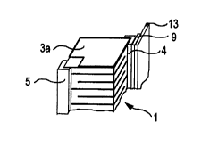
Figure 2 shows an exemplary piezoelectric
actuator in cross-section through the plane of an inner
electrode. In the Figure, the actuator is illustrated
with a square outline, but may also have any other
arbitrary shapes. The uppermost electrode layer 3a has a
cut-out in the left upper corner, at which the
piezoceramic layer 2 lying underneath is visible. This
cut-out may have not only a square dimension, as shown,
but also a rectangular or elliptical or circular
dimension, and may be arranged not only at the corner but
also in the centre of the actuator side. The electrode
layer 3a is electrically conductively connected to the
metallization strip 4, which here is applied at the
corner. The metallization strip 5 applied at the apposite
corner has no contact with the electrode layer 3a,
because of the cut-out in the latter. On the other hand,
it is connected to the electrode layer 3b lying under-
neath (not visible here), which has at the opposite
corner of the actuator the cut-out that is illustrated
with dashed lines and designated by 8.
According to the invention, the metallization
strips 4 and 5 are now connected to a contact tab 13. The
connection is carried out over the entire height of the
stack or at least over the entire height of the electrode
layers 3 to be contacted. The contact tab 13 is applied
with the aid of a connecting means 9, for example a
conductive adhesive or a solder layer. The contact tab 13
has a projecting region with respect to the stack or the
connection to the metallization strip 4, the length b of
this region being adequate for cracks in the
metallization strip occurring during the operation or the
polarization of the piezoelectric actuator 1 to run out
within the contact tab 13. For exemplary piezoelectric
actuators having a basic area of 7 x 7 mm and a height of
up to 40 mm, it is sufficient if the projecting region
has a width b of 5 to 10 mm. At lower stack heights, the
width of the projecting region b can also be selected to
CA 02271281 1999-OS-10
GR 96 P 2495 - 10 -
be smaller.
At the end of the projecting region b, the
further contacting can be performed in any desired way,
for example by soldering on a wire, in order to lead
further to the electrical connections 6 and 7.
In the same way, the second metallization strip
5 is connected to a contact tab 13 of identical type.
Laser-beam soldering is used as the preferred application
method.
Figure 3 shows, in the form of a detail and in a
perspective schematic illustration, a piezoelectric
actuator 1 having a fitted contact tab 13. Although the
piezoelectric actuator illustrated has a lengthwise
expansion, it is not suitable for the transmission of
large forces. For this purpose, piezoelectrically
inactive end plates, not illustrated here, are required
on the upper and lower sides of the piezoelectric
actuator 1, and are likewise monolithically joined to the
stack.
Figure 4 shows the simplest embodiment of a
contact tab in a schematic cross-section, in which the
contact tab comprises only one electrically conductive
layer, for example a metal foil 10. Optionally, the
electrically conductive layer (foil) 10 may already be
coated along one edge with solder 9 or another
electrically conductive connecting means, which is used
for the connection to the metallization strips 4 and 5.
The length of the contact tab vertically in relation to
the illustrated section plane corresponds, for example,
to the stack height of the piezoelectric actuator 1,
whereas the width of the contact tab 13 or of the film 10
corresponds at least to the width b of the projecting
region plus the width of the connection to the
metallization strips. For the piezoelectric actuators of
7 x 7 x 40 (mm)3, cited by way of example, a projecting
region b of 5 to 10 mm is adequate.
Figure 5 shows a further design of the contact
tab 13, in which the latter comprises a composite
material made of a carrier 11 and an electrically
CA 02271281 1999-OS-10
GR 96 P 2495 - 11 -
conductive layer 10. The carrier 11 used is, for example,
a plastic film that is coated with an electrically highly
conductive metal 10. In one embodiment of the invention,
a Kapton~ film of 25 ~.m thickness, for example, is used
as the carrier 11, which is coated with a suitable metal,
for example with 25 ~.m of copper. As connecting means 9,
a tin layer 9 is applied, for example by means of
electroplating. The use of copper for the electrically
conductive layer 10 has the advantage of good
solderability and of high electrical conductivity.
Figure 6: In a further refinement of the
invention, the contact tab 13 is designed to be similar
to that in Figure 5, but in addition to the solder strip
9 further has an insulating layer 12 with which virtually
the entire surface of the electrically conductive layer
10 is covered or laminated. This insulating layer 12 may
be a further plastic layer, which directly adjoins the
solder strip 9 or, as illustrated, is spaced apart from
this.
If laser-beam soldering is used as the
application method, then it is particularly advantageous
if the contact tabs according to Figures 5 and 6 comprise
a carrier 11 that is transparent to the wavelength of the
laser used, for example the Kapton film mentioned. In
this way, the laser-beam soldering can be carried out
with the lowest expenditure of energy, the laser energy
being able to be coupled virtually completely into the
solder 9 to be melted. Thermal loading of the film 11 or
of the piezoelectric actuator 1 is avoided in this case.