Note: Descriptions are shown in the official language in which they were submitted.
CA 02271536 1999-OS-12
AT9-98-081 1
NON-UNIFORM MEMORY ACCESS (NUMA) DATA PROCESSING SYSTEM THAT
BUFFERS POTENTIAL THIRD NODE TRANSACTIONS TO DECREASE
COMMUNICATION LATENCY
BACKGROUND OF THE INVENTION
1. Technical Field:
The present invention relates in general to a method and system for data
processing and, in
particular, to a non-uniform memory access (NUMA) data processing system and
method of
communication in a NUMA data processing system. Still more particularly, the
present invention
s relates to a NUMA data processing system and method of communication in
which potential third
node transactions are buffered to reduce communication latency.
2. Description of the Related Art:
It is well-known in the computer arts that greater computer system performance
can be
achieved by harnessing the processing power of multiple individual processors
in tandem. Multi-
processor (MP) computer systems can be designed with a number of different
topologies, of which
various ones may be better suited for particular applications depending upon
the performance
requirements and software environment of each application. One of the most
common MP computer
topologies is a symmetric mufti-processor (SMP) configuration in which
multiple processors share
common resources, such as a system memory and input/output (I/O) subsystem,
which are typically
coupled to a shared system interconnect. Such computer systems are said to be
symmetric because
all processors in an SMP computer system ideally have the same access latency
with respect to data
stored in the shared system memory.
Although SMP computer systems permit the use of relatively simple inter-
processor
zo communication and data sharing methodologies, SMP computer systems have
limited scalability.
In other words, while performance of a typical SMP computer system can
generally be expected to
improve with scale (i.e., with the addition of more processors), inherent bus,
memory, and
CA 02271536 1999-OS-12
AT9-98-081 2
input/output (I/O) bandwidth limitations prevent significant advantage from
being obtained by
scaling a SMP beyond a implementation-dependent size at which the utilization
of these shared
resources is optimized. Thus, the SMP topology itself suffers to a certain
extent from bandwidth
limitations, especially at the system memory, as the system scale increases.
SMP computer systems
s also do not scale well from the standpoint ofmanufacturing efficiency. For
example, although some
components can be optimized for use in both uniprocessor and small-scale SMP
computer systems,
such components are often inefficient for use in large-scale SMPs. Conversely,
components
designed for use in large-scale SMPs are impractical for use in smaller
systems from a cost
standpoint.
As a result, an MP computer system topology known as non-uniform memory access
(NUMA) has emerged as an alternative design that addresses many of the
limitations of SMP
computer systems at the expense of some additional complexity. A typical NUMA
computer system
includes a number of interconnected nodes that each include one or more
processors and a local
"system" memory. Such computer systems are said to have a non-uniform memory
access because
1s each processor has lower access latency with respect to data stored in the
system memory at its local
node than with respect to data stored in the system memory at a remote node.
NUMA systems can
be further classified as either non-coherent or cache coherent, depending upon
whether or not data
coherency is maintained between caches in different nodes. The complexity of
cache coherent
NUMA (CC-NUMA) systems is attributable in large measure to the additional
communication
zo required for hardware to maintain data coherency not only between the
various levels of cache
memory and system memory within each node but also between cache and system
memories in
different nodes. NUMA computer systems do, however, address the scalability
limitations of
conventional SMP computer systems since each node within a NUMA computer
system can be
implemented as a smaller SMP system. Thus, the shared components within each
node can be
25 optimized for use by only a few processors, while the overall system
benefits from the availability
of larger scale parallelism while maintaining relatively low latency.
A principal performance concern with CC-NUMA computer systems is the latency
associated
with communication transactions transmitted via the interconnect coupling the
nodes. Because all
CA 02271536 1999-OS-12
AT9-98-081 3
data accesses can potentially trigger a coherency or data request transaction
on the nodal
interconnect, the latency associated with the transmission of requests to
remote nodes and
transmission of the responses from the remote nodes can dramatically influence
overall system
performance. As should thus be apparent, it would be desirable to provide a CC-
NUMA computer
system having low inter-node communication latency.
SUMMARY OF THE INVENTION
It is therefore one object of the present invention to provide an improved
method and system
for data processing.
It is another object of the present invention to provide an improved NUMA data
processing
system and method of communication in a NUMA data processing system.
It is yet another object of the present invention to provide an improved NUMA
data
processing system and method of communication in which potential third node
transactions are
buffered to reduce communication latency.
The foregoing objects are achieved as is now described. A non-uniform memory
access
(NUMA) computer system is provided that includes an interconnect to which
first, second, and third
processing nodes are coupled. Each of the first, second, and third processing
nodes includes at least
one processor and a local system memory. The NUMA computer system further
includes a
transaction buffer, coupled to the interconnect, that stores communication
transactions transmitted
ao on the interconnect that are both initiated by and targeted at a processing
node other than the third
processing node. In response to a determination that a particular
communication transaction
originally targeting another processing node should be processed by the third
processing node, buffer
control logic coupled to the transaction buffer causes the particular
communication transaction to
be retrieved from the transaction buffer and processed by the third processing
node. In one
a5 embodiment, the interconnect includes a broadcast fabric, and the
transaction buffer and buffer
control logic form a portion of the third processing node.
The above as well as additional obj ects, features, and advantages of the
present invention will
become apparent in the following detailed written description.
CA 02271536 1999-OS-12
AT9-98-081 4
BRIEF DESCRIPTION OF THE DRAWINGS
The novel features believed characteristic of the invention are set forth in
the appended
claims. The invention itself however, as well as a preferred mode of use,
further objects and
advantages thereof, will best be understood by reference to the following
detailed description of an
illustrative embodiment when read in conjunction with the accompanying
drawings, wherein:
Figure 1 depicts an illustrative embodiment of a NUMA computer system with
which the
present invention may advantageously be utilized;
Figure 2A is a more detailed block diagram of an interconnect architecture
utilized in the
illustrative embodiment shown in Figure 1;
Figure 2B depicts an illustrative embodiment of an I-command;
Figure 2C is a more detailed block diagram of the node controller shown in
Figure 1;
Figures 3A-3D illustrate a third node communication scenario in accordance
with the prior
art; and
Figure 4 is a high level logical flowchart of a third node communication
methodology in
accordance with the present invention.
DETAILED DESCRIPTION OF ILLUSTRATIVE EMBODIMENT
Svstem Overview
With reference now to the figures and in particular with reference to Figure
1, there is
2o depicted an illustrative embodiment of a NUMA computer system in accordance
with the present
invention. The depicted embodiment can be realized, for example, as a
workstation, server, or
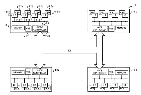
mainframe computer. As illustrated, NUMA computer system 8 includes a number
(N) of
processing nodes l0a-lOd, which are interconnected by node interconnect 22.
Processing nodes
l0a-lOd each include at least one, and up to M, processors 12. Processors 12a-
12d are preferably
zs identical and may comprise a processor within the PowerPCT"~ line of
processors available from
International Business Machines (IBM) Corporation of Armonk, New York. In
addition to the
registers, instruction flow logic and execution units utilized to execute
program instructions, each
of processors 12a-12d also includes an on-chip level one (L 1 ) cache (not
illustrated), which together
CA 02271536 1999-OS-12
AT9-98-081 5
with a respective one of level two (L2) caches 14a-14d is utilized to stage
data to the associated
processor 12 from system memories 18. In other words, the L1 caches and L2
caches 14a-14d
function as intermediate storage between the system memories 18 and processors
12 that temporarily
buffer data that are likely to be accessed by the associated processor 12. L2
caches 14 typically have
s a much larger storage capacity than the L 1 caches, but at a longer access
latency. For example, L2
caches 14a-14d may have a storage capacity of I-16 megabytes (MB), while the
on-chip L1 caches
may have a storage capacity of 8-32 kilobytes. Although L2 caches 14a-14d are
illustrated in
Figure 1 as external to processors 12, it should be understood that L2 caches
14a-14d could
alternatively be incorporated within the associated processor 12 as an
additional level of on-chip
cache memory. Furthermore, it should be understood that one or more additional
levels of cache
memory (L3, L4, etc.) could be utilized to provide additional data storage. In
the following
discussion, each processor 12 and its associated cache hierarchy (L1, L2,
etc.) is considered to be
a single snooper.
As shown, processing nodes l0a-lOd further include a respective node
controller 20, which,
m together with system memory 18 and L2 caches 14a-14d, is coupled to local
interconnect 16. Each
node controller 20 serves as a local agent for remote processing nodes 10 by
performing at least two
functions. First, node controllers 20 snoop the associated local interconnect
16 and facilitate the
transmission of local communication transactions to remote processing nodes
10. Second, node
controllers 20 snoop communication transactions on node interconnect 22 and
master relevant
z o communication transactions on the associated local interconnect 16.
Communication on each local
interconnect 16 is controlled by an arbiter 24. As discussed further below,
arbiters 24 regulate access
to local interconnects 16 based on bus request signals generated by processors
12 and compile
coherency responses for snooped communication transactions on local
interconnects 16.
Of course, NUMA computer system 8 can further include additional devices that
are not
a s necessary for an understanding of the present invention and are
accordingly omitted in order to avoid
obscuring the present invention. For example, each node 10 may also support
I/O devices (e.g., a
display device, keyboard, or graphical pointer), non-volatile storage for
storing an operating system
and application software, and serial and parallel ports for connection to
networks or attached devices.
CA 02271536 1999-OS-12
AT9-98-081 6
Memory Organization
All of processors 12 in NUMA computer system 8 share asingle physical memory
space,
meaning that each physical address is associated with only a single location
in one of system
memories 18. Thus, the overall contents of the system memory, which can
generally be accessed
s by any processor 12 in NUMA computer system 8, can be viewed as partitioned
between the four
system memories 18. For example, for the illustrative embodiment of the
present invention shown
in Figure 1, processors 12 address a 16 gigabyte (GB) address space including
both a general
purpose memory area and a reserved area. The general purpose memory area is
divided into 500 MB
segments, with each of the four processing nodes 10 being allocated every
fourth segment. The
to reserved area, which may contain approximately 2 GB, includes system
control and peripheral
memory and I/O areas that are each allocated to a respective one of processing
nodes 10.
For purposes of the present discussion, the processing node 10 that stores a
particular datum
in its system memory 18 is said to be the home node for that datum;
conversely, others of processing
nodes 10-lOd are said to be remote nodes with respect to the particular datum.
Memory Coherency
Because data stored within each system memory 18 can be requested, accessed,
and modified
by any processor 12 within NUMA computer system 8, NUMA computer system 8
implements a
cache coherency protocol to maintain coherency both between caches in the same
processing node
zo and between caches in different processing nodes. Thus, NUMA computer
system 8 is properly
classified as a CC-NUMA computer system. The cache coherence protocol that is
implemented is
implementation-dependent and may comprise, for example, the well-known
Modified, Exclusive,
Shared, Invalid (MESI) protocol or a variant thereof. Hereafter, it will be
assumed that L 1 caches,
L2 caches 14b, and arbiters 24 implement the conventional MESI protocol, of
which node
controllers 20 recognize the M, S and I states and consider the E state to be
merged into the M state
for correctness. That is, node controllers 20 assume that data held
exclusively by a remote cache has
been modified, whether or not the data has actually been modified.
CA 02271536 1999-OS-12
AT9-98-081 7
Interconnect Architecture
Local interconnects 16 and node interconnect 22 can each be implemented with
any
broadcast or point-to-point interconnect architecture, for example, a bus or
crossbar switch.
However, in a preferred embodiment, each of local interconnects 16 and node
interconnect 22 is
s implemented as a hybrid-bus architecture governed by the 6xx communication
protocol developed
by IBM Corporation.
Refernng now to Figure 2A, a preferred embodiment of node interconnect 22
within NUMA
computer system 8 is illustrated from the perspective of one of processing
nodes 10. As shown, the
illustrated embodiment of node interconnect 22 includes separate (i.e., non-
multiplexed) address and
data portions, which are decoupled to permit split transactions. The address
portion of node
interconnect 22 is implemented as a shared address bus 26, access to which is
controlled by central
arbiter 27. A node controller 20 requests access to shared address bus 26 by
asserting its respective
address bus request (ABR) signal 25 and is informed of a grant of access by
central arbiter 27
through the assertion of its respective address bus grant (ABG) signal 29.
Each node controller 20
coupled to node interconnect 22 also snoops all communication transactions on
shared address bus
26 to support memory coherency, as discussed further below. A summary of
relevant signal names
and definitions for shared address bus 26 is given in Table I.
CA 02271536 1999-OS-12
AT9-98-081
TABLE I
Signal Name No. of Description
lines
Address <0:7> 8 Address bus modifiers defining
attributes
of a communication transaction
for
coherency, write thru, and
protection
Address <8:15> 8 Tag used to identify a communication
transaction
Address <16:63> 48 Address signals that indicate
the physical,
virtual or I/O address in
a request
AParity <0:2> 3 Indicates parity for address
bits <0:63>
TDescriptors 10 Indicate size and type of
communication
transaction
The utilization of shared address bus 26 is preferably enhanced by
implementing shared address bus
26 as a pipelined bus, meaning that a subsequent transaction can be sourced by
a processing node
prior to the master of a previous communication transaction receiving
coherency responses from
each of the other processing nodes 10.
While the data portion of node interconnect 22 could also be implemented as a
shared bus,
~s the data portion of node interconnect 22 is preferably implemented as a
distributed switch having
N-1 (e.g., 4-1=3) data-in channels 34 and a single data-out channel 32 for
each processing node 10.
The data output by a processing node 10 on data-out channel 32 are transmitted
to all of processing
nodes 10, and each processing node 10 receives data from each of the other
processing nodes 10 via
data-in channels 34. By implementing the data portion of node interconnect 22
in this manner rather
2 o than as a shared bus, deadlocks are avoided and data bandwidth is
advantageously increased. The
relevant signal names and definitions for each channel within the preferred
embodiment of the data
portion of node interconnect 22 are summarized below in Table II.
TABLE II
CA 02271536 1999-OS-12
AT9-98-081 9
Signal Name No. of Description
lines
Data <0:127> 128 Data lines used to carry data
for read and
write transactions
Data parity <0:15> 16 Indicate parity for data lines
<0:127>
DTag <0:7> 8 Tag used to match a data packet
with an
address bus transaction
s DValid <0:1> 2 Indicate if valid information
is present on
Data and DTag lines
As indicated in Table II, to permit recipients of data packets to determine
the communication
transaction to which each data packet belongs, each data packet is identified
with a transaction tag.
This permits the timings of shared address bus 26 and the data portion of node
interconnect 22 to
be completely decoupled, meaning that no fixed timing relationship exists
between address tenures
and data tenures and that data tenures can be ordered differently than the
corresponding address
tenures. Those skilled in the art will appreciate that data flow control logic
and associated flow
control signals should be utilized to regulate use of the finite data
communication resources.
As illustrated in Figure 2A, a preferred embodiment of node interconnect 22
also includes
15 a high speed I-command channel 31. This sideband channel, like the data
portion of node
interconnect 22, is preferably implemented as a distributed switch including
one output channel
(command-out channel 32) and N-1 input channels (command-in channels 34) for
each processing
node 10. Channels 32 and 34 permit the communication of I-commands between
processing nodes
without creating additional loading on the address or data portions of node
interconnect 22. An
2o exemplary embodiment of an I-command is shown in Figure 2B. As illustrated,
I-command 36
includes five (5) fields: a 4-bit command type field 33, an N-bit (e.g., 4-
bit) target node field 35, an
N-bit source node field 37, a transaction tag field 38, and a valid (V) field
39. Command type field
33 provides an encoded indication of the type of I-command 36. Some of the
possible I-commands
that can be encoded within type field 33 are listed below in Table III.
CA 02271536 1999-OS-12
AT9-98-081 10
TABLE III
I-command I-command typesMeaning
groups
s commands 3rd node run Run buffered transaction at
third (target)
node
Error Error detected in transaction
Reissue Reissue transaction to source
node
coherency Retry Retry transaction -- usually
responses for flow
control reasons
Modified Line is modified in cache and
intervention will be
sourced to target node
Shared Line is held shared in cache
Null Line is invalid in cache
For each type of I-command, the recipient is specified in target node field
35, the sending node is
specified in source node field 37, and the transaction to which the I-command
relates is specified
within transaction tag field 38. The validity of I-command 36 is indicated by
valid (V) field 39.
Importantly, the I-commands issued by processing nodes 10 via I-command
channel 31 do not have
any necessary timing relationship with the address or data tenures of the
associated communication
transactions. And, because I-command channel 31 utilizes small packets and is
non-blocking (i.e.,
15 use of I-command channel 31 by one processing node 10 does not inhibit or
block usage by other
processing nodes), I-commands can be transmitted at high speed between
processing nodes 10.
Like node interconnect 22, local interconnects 16 include three distinct
components -- an
address portion, a data portion, and a coherency portion. The address portion
of each local
interconnect 22 is preferably implemented as described above with respect to
shared address bus 26
zo of node interconnect 22. The data portion of each local interconnect 16
utilizes the same data signals
listed above in Table II, but is preferably implemented as a shared data bus
rather than a distributed
switch (although either could be utilized). In lieu of the I-command channel
discussed above, the
CA 02271536 1999-OS-12
AT9-98-081 11
coherency portion of each local interconnect 16 includes signal lines coupling
each attached snooper
to the local arbiter 24. The signal lines within local interconnects 16 that
are utilized for coherency
communication are summarized below in Table V.
s TABLE IV
Signal Name No. of Description
lines
AStatOut <0:1 > 2 Encoded signals asserted by
each bus
receiver to indicate flow control
or error
information to arbiter
AStatIn <0:1 > 2 Encoded signals asserted by
arbiter in
response to tallying the AStatOut
signals
asserted by the bus receivers
ARespOut <0:2> 3 Encoded signals asserted by
each bus
receiver to indicate coherency
information to arbiter
ARespIn <0:2> 3 Encoded signals asserted by
arbiter in
response to tallying the ARespOut
signals asserted by the bus
receivers
In contrast to the coherency responses transmitted between processing nodes 10
via I-command
channel 31, coherency responses transmitted via the AResp and AStat lines of
local interconnects
~s 16 preferably have a fixed but programmable timing relationship with the
associated address bus
transactions. For example, the AStatOut votes, which provide a preliminary
indication of the
response of each snooper to a communication transaction on the local address
bus, may be required
in the second cycle following receipt of a request on the local address bus.
Arbiter 24 compiles the
AStatOut votes and then issues the AStatIn vote a fixed but programmable
number of cycles later
zo (e.g., 1 cycle). Possible AStat votes are summarized below in Table V.
CA 02271536 1999-OS-12
AT9-98-081 12
TABLE V
AStat vote Meaning
Null Idle
Ack Transaction accepted by snooper
Error Parity error detected in transaction
Retry Retry transaction, usually for flow
control
Following the AStatIn period, the ARespOut votes may then be required a fixed
but programmable
number of cycles (e.g., 2 cycles) later. Arbiter 24 also compiles the ARespOut
votes of each snooper
and delivers an ARespIn vote, preferably during the next cycle. The possible
AResp votes
preferably include the coherency responses listed above in Table III. In
addition, the possible AResp
votes include "ReRun," which is issued (usually by a node controller 20) to
indicate that the snooped
request has a long latency and that the source of the request will be
instructed to reissue the
~s transaction at a later time. Thus, in contrast to a retry response, a ReRun
response makes the
recipient of a transaction that voted ReRun (and not the originator of the
transaction) responsible for
causing the communication transaction to be reissued at a later time.
Node Controller
zo Refernng now to Figure 2C, there is illustrated a more detailed block
diagram of a node
controller 20 in NUMA computer system 8 of Figure 1. As shown in Figure 2C,
each node
controller 20, which is coupled between a local interconnect 16 and node
interconnect 22, includes
transaction receive unit 40, transaction send unit 42, a data receive unit
(DRU) 44, and a data send
unit (DSU) 46. Transaction receive unit 40, transaction send unit 42, DRU 44
and DSU 46 can be
zs implemented, for example, with field programmable gate arrays (FPGAs) or
application specific
integrated circuits (ASICs). As indicated, the address and data paths through
node controller 20 are
bifurcated, with address signals being processed by transaction receive unit
40 and transaction send
unit 42 and data signals being processed by DSU 44 and DRU 46.
CA 02271536 1999-OS-12
AT9-98-081 13
Transaction receive unit 40, which is so designated to indicate transaction
flow off of node
interconnect 22, is responsible for receiving I-commands from I-command
channel 31, accepting
transactions and responses from node interconnect 22, issuing received
transactions on local
interconnect 16, and forwarding responses to transaction send unit 42.
Transaction receive unit 40
s is also responsible for maintaining transaction buffer 52. Transaction
buffer 52 is an associative
buffer in which transaction receive unit 40 stores communication transactions
snooped on shared
address bus 26 that are sourced by and targeted at processing nodes 10 other
than the local
processing node. Each entry in transaction buffer 52 stores a communication
transaction in
association with a transaction tag (i.e., address bits <8:15>) so that the
communication transactions
can be rapidly accessed, as discussed below with respect to Figure 4.
Transaction send unit 42, which as indicated by its nomenclature is a conduit
for transactions
flowing onto node interconnect 22, interacts with transaction receive unit 40
to process memory
request transactions and issues commands to DRU 44 and DSU 46 to control the
transfer of data
between local interconnect 16 and the data portion of node interconnect 22.
Transaction send unit
~s 42 also implements the selected (i.e., MSI) coherency protocol for node
interconnect 22 and
maintains coherence directory 50.
Coherence directory 50 stores indications of the system memory addresses of
data (e.g.,
cache lines) checked out to caches in remote nodes for which the local
processing node is the home
node. The address indication for each datum is stored in association with an
identifier of each
zo processing node having a copy of the datum and the coherency status of the
datum at each such
processing node. Possible coherency states for entries in coherency directory
50 are summarized in
Table VI.
CA 02271536 1999-OS-12
AT9-98-081 14
TABLE VI
Coherence Possible Possible Meaning
directory states) states)
in in
state local cacheremote
cache
Modified I M,E, or Cache line may be modified
(M) I at a
remote node with respect
to
system memory at home
node
Shared (S) S or I S or I Cache line may be held
non-
exclusively at remote
node
Invalid M,E,S, I Cache line is not held
(I) or I by any
remote node
Pending- S or I S or I Cache line is in the process
of
shared being invalidated at remote
nodes
to Pending- I M,E, or Cache line, which may
I be
modified modified remotely, is
in process
of being written back
to system
memory at home node, possibly
with invalidation at remote
node
As indicated in Table VI, the knowledge of the coherency states of cache lines
held by remote
processing nodes is imprecise. This imprecision is due to the fact that a
cache line held remotely can
~s make a transition from S to I, from E to I, or from E to M without
notifying the node controller 20
of the home node.
Prior Art "Third Node" Communication Scenario
With reference now to Figures 3A-3D, there is depicted an exemplary "third
node"
zo communication scenario within a NUMA computer system in accordance with the
prior art. As
shown, conventional NUMA computer system 58 includes first, second, third, and
fourth nodes,
which are respectively illustrated at reference numerals 60, 62, 64, and 66.
Assuming that second
node 62 is the home node for data that is held exclusively (i.e., in E or M
state) by third node 64, first
node 60 requests the data by broadcasting a read request on the node
interconnect. As shown in
CA 02271536 1999-OS-12
AT9-98-081 15
Figure 3A, the request transaction is received by second node 62, third node
64, and fourth node 66;
however, because the requested data is owned by second node 62, third node 64
and fourth node 66
filter out (i.e., ignore) the data request. In response to receipt of the
request transaction, second node
62 checks its node directory to determine if a copy of the requested data is
held within a remote
s node. Because the requested data is recorded in the node directory of second
node 62 as held
exclusively by a remote node, second node 62 is unable to immediately respond
to the request
transaction received from first node 60. This is because the copy of the
requested data at second
node 62 may be stale (i.e., a processor in third node 64 may have modified the
requested data).
Accordingly, as shown in Figure 3B, second node 62 issues to third node 64,
via the node
interconnect, a request transaction specifying the address of the requested
data. As indicated by
arrow 70, in response to the request transaction third node 64 forwards the
request transaction to
internal caches that may store the requested data. The internal cache holding
the requested data
exclusively responds with a shared coherency response, indicating that the
cache will update the
coherency state of the requested data to S state. Then, as shown in Figure 3C,
third node 64
~s transmits a shared response to second node 62, informing second node 62
that the coherency state
of the copy of the requested data held by third node 64 is being updated to
the shared state.
Finally, referring to Figure 3D, in response to receipt of the shared response
from third node
64, second node 62 is able to process the request transaction as illustrated
by arrow 72. The
requested data is then sourced to first node 60 with a shared coherency state,
as indicated by arrow
zo 74. While this conventional third node communication scenario ensures data
coherency between
nodes in a NUMA computer system, it should be noted that the same
communication transaction is
transmitted to third node 64 twice, as shown in Figures 3A and 3B. The present
invention
advantageously eliminates this redundant communication via the node
interconnect, thereby reducing
communication latency and enhancing the scalability of a NUMA computer system.
zs
Innovative Third Node Communication Scenario
Refernng now to Figure 4, there is illustrated a high level logical flowchart
of a third node
communication methodology in accordance with the present invention. The
flowchart shown in
CA 02271536 1999-OS-12
AT9-98-081 16
Figure 4 assumes the same initial conditions as the exemplary prior art
scenario discussed supra,
namely, that one of processors 12a-12d has issued a read request for a cache
line that is held
exclusively by processing node lOc and has processing node lOb as a home node.
As depicted, the process begins at block 80 and thereafter proceeds to block
82, which
illustrates the node controller 20 of processing node l0a transmitting, via
shared address bus 26 of
node interconnect 22, a communication transaction requesting data at a
specified address. Because
shared address bus 26 is a broadcast medium in the preferred embodiment, the
request transaction
is received by each of processing nodes l Ob, l Oc and l Od. Following block
82, the process proceeds
both to blocks 84-88 and to block 90.
Blocks 84-88 illustrate the processing performed by processing node l Ob (i.
e., the home node
of the requested cache line) in response to receipt of the request transaction
on shared address bus
26. First, as shown at block 84, node controller 20 of processing node lOb
arbitrates for ownership
of its local interconnect 16 and masters the request transaction on local
interconnect 16. The process
then proceeds to block 86, which depicts node controller 20 of processing node
lOb voting ReRun
for its ARespOut coherency response to the request transaction. The ReRun vote
indicates that
transaction send unit 42 has determined by reference to coherence directory 50
that the coherency
state of the requested cache line cannot be resolved without involving a third
processing node,
namely, processing node lOc, which holds the requested data exclusively. As
shown at block 88,
in response to arbiter 24 of local interconnect 16 voting ReRun for ARespIn,
transaction send unit
zo 42 within node controller 20 of processing node lOb issues to processing
node lOc, via I-command
channel 31, a "3rd node run" I-command in conjunction with the transaction tag
of the original
request transaction issued by processing node 10a. Because the I-command is
transmitted via
sideband I-command channel 31 rather than the address or data portions of node
interconnect 22, the
address bandwidth of node interconnect 22 that would otherwise be consumed can
be
25 advantageously utilized to communicate other transactions. In this manner,
communication latency
on the blocking, bandwidth-limited portions of node interconnect 22 is
reduced. Following block
88, the process passes to block 100, which is described below.
Block 90 illustrates the processing triggered at processing nodes lOc and lOd,
which are each
CA 02271536 1999-OS-12
AT9-98-081 17
neither the source nor target of the request transaction, in response to
receipt of the request
transaction issued by processing node 10a. As indicated, transaction receive
unit 40 within each of
processing nodes lOc and lOd stores the request transaction and transaction
tag in an entry within
its respective transaction buffer 52. In a preferred embodiment, not all
snooped transactions are
stored in the transaction buffers 52 of third nodes (i.e., processing nodes
that are neither the source
nor the target of a transaction). Instead, in order to conserve the limited
storage capacity of
transaction buffers 52, only transactions identified by address signal lines
<0:7> and the
TDescriptors as transactions that could possibly require third node
involvement are buffered. Of
course, other optimizations to improve the storage efficiency of limited-size
transaction buffers 52
are possible, such as storing only those transactions that would entail the
use of greater than a
threshold amount of communication resources for retransmission if not
buffered.
The process proceeds from block 90 to block 100, which illustrates a
determination of
whether or not processing node lOc, the third node, has received a "3rd node
run" I-command. If
not, the process illustrated in Figure 4 iterates at block 100 until a "3rd
node run" I-command is
received by processing node lOc. Of course, during the interval between the
recordation of the
request transaction by processing node lOc in transaction buffer 52 and the
receipt of a "3rd node
run" I-command by processing node lOc, processing nodes l0a-lOd can initiate,
receive and process
other communication transactions. Then, in response to a determination at
block 100 that processing
node lOc has received a "3rd node run" I-command, the process passes to block
102.
ao Block 102 illustrates a determination by transaction receive unit 40 within
node controller
20 of processing node lOc whether or not a transaction tag matching the
transaction tag received via
I-command channel 31 is stored within transaction buffer 52. Depending upon
the size of
transaction buffer 52 and the number of communication transactions received by
processing node
lOc between steps 90 and 102, the transaction specified by the transaction tag
may no longer be
zs stored within transaction buffer 52 due to its limited size. If a
transaction having a matching
transaction tag is stored within transaction buffer 52, the process proceeds
from block 102 to block
108, which is described below. However, in response to a determination that
the transaction tag
received via I-command channel 31 does not match any of the transactions tags
in transaction buffer
CA 02271536 1999-OS-12
AT9-98-081 18
52, the process proceeds to block 104. Block 104 depicts processing node lOc
transmitting a
"Reissue" I-command to processing node lOb via I-command channel 31 in
conjunction with the
received transaction tag. As shown at block 106, in response to receipt of the
"Reissue" I-command,
processing node lOb retransmits the communication transaction to processing
node lOc via shared
s address bus 26 of node interconnect 22, as described above with respect to
Figure 3B. Thus, in the
statistically unlikely event that the relevant communication transaction is
not stored in transaction
buffer 52 of processing node lOc, NUMA computer system 8 handles a third node
communication
scenario like conventional NUMA computer system 58.
The process proceeds from either block 102 or block 106 to block 108, which
illustrates
transaction receive unit 40 within node controller 20 of processing node lOc
mastering the request
transaction (which was accessed from transaction buffer 52 or received from
processing node lOb)
on local interconnect 16 of processing node lOc. In response to the request
transaction, each of the
snoopers attached to node interconnect 16 votes a coherency response during
the ARespOut period.
The snooper holding the requested data exclusively votes shared during the
ARespOut period and
initiates an update to the coherency status of the requested cache line to S
state; meanwhile, other
snoopers vote null. As depicted at block 110, bus arbiter 24 of processing
node lOc compiles these
coherency responses and issues a shared coherency response during the ARespIn
period. In response
to receipt of the shared ARespIn coherency response, transaction send unit 42
within node controller
20 transmits an I-command containing a shared response and the transaction tag
to processing node
zo lOb via I-command channel 31. The process then proceeds to block 112, which
depicts node
controller 20 of processing node lOb ReRunning the request transaction on
local interconnect 16 of
processing node lOb. In response to snooping the ReRun request transaction,
node controller 20 of
processing node lOb votes shared during the ARespOut period, indicating that
processing node lOc
holds the requested data in shared state. Bus arbiter 24 of processing node
lOb thereafter compiles
zs the coherency responses and votes shared during the ARespIn period.
Finally, as shown at block
114, node controller 20 of processing node lOb transmits an I-command
containing a shared
response and the transaction tag to processing node l0a via I-command channel
31 and sources the
requested cache line to processing node l0a via data-out channel 28.
Thereafter, the process
CA 02271536 1999-OS-12
AT9-98-081 19
terminates at block 116.
As has been described, the present invention provides an improved NUMA
computer system
and an improved third node communication methodology in a NUMA computer
system. In
accordance with the present invention, transactions that could possibly
require third node
s involvement are buffered at a third node that is neither the source nor
target of a communication
transaction. In the event that involvement of the third node is required, the
transaction can be
accessed from the buffer rather than retransmitted over the shared address bus
within the node
interconnect. In this manner, traffic on the bandwidth-limited portion of node
interconnect is
advantageously reduced, thereby decreasing communication latency and enhancing
overall system
performance.
While the invention has been particularly shown and described with reference
to a preferred
embodiment, it will be understood by those skilled in the art that various
changes in form and detail
may be made therein without departing from the spirit and scope of the
invention. For example,
while the present invention has been described with respect to a preferred
embodiment in which node
interconnect is a bus-based fabric (e.g., shared bus), it should be understood
that in alternative
embodiments the node interconnect could be implemented with a point-to-point
broadcast fabric,
such as a crossbar switch. In this embodiment, the transaction buffer for each
node and the
associated control logic would be coupled to the crossbar switch rather than
incorporated within each
node.