Note: Descriptions are shown in the official language in which they were submitted.
CA 02271541 1999-OS-19
MULTIPLE DATA SURFACE OPTICAL DATA STORAGE SYSTEM
Background of the Invention
Field of the Invention
This invention relates generally to optical data storage systems and more
specifically to a
storage system having multiple data storage surfaces.
Description of the Prior Art
Optical data storage systems provide a means for storing great quantities of
data on a disk.
The data is accessed by focussing a laser beam onto the data layer of the disk
and then detecting
the reflected light beam. Various kinds of systems are known. In a ROM (Read
Only Memory)
system, data is permanently embedded as marks in the disk at the time of
manufacture of the
disk. The data is detected as a change in reflectivity as the laser beam
passes over the data
marks. A WORM (Write-Once Read Many) system allows the user to write data by
making
marks, such as pits, on a blank optical disk surface. Once the data is
recorded onto the disk it
cannot be erased. The data in a WORM system is also detected as a change in
reflectivity.
Erasable optical systems are also known. These systems use the laser to heat
the data
layer above a critical temperature in order to write and erase the data.
Magneto-optical recording
systems record data by orienting the magnetic domain of a spot in either an up
or a down
position. The data is read by directing a low power laser to the data layer.
The differences in
magnetic domain direction cause the plane of polarization of the light beam to
be rotated one
way or the other, clockwise or counterclockwise. This change in orientation of
polarization is
then detected. Phase change recording uses a structural change of the data
layer itself
(amorphous/crystalline are two common types of phases) to record the data. The
data is detected
as changes in reflectivity as a beam passes over the different phases.
In order to increase the storage capacity of an optical disk, multiple data
layer systems have
been proposed. An optical disk having two or more data layers may in theory be
accessed at
different layers by changing the focal position of the lens. Examples of this
approach include US
Patent 3,946,367 issued March 23, l976 by Wohlmut, et al.; US Patent 4,2l9,704
issued August
26, 1980 to Russell; US Patent 4,450,553 issued May 22, l984 to Holster, et
al.; US 4,905,215
issued February 27, 1990 to Hattori, et al.; Japanese Published Application,
63-276732
published November 15, 1988 by Watanabe, et al.; and IBM Technical Disclosure
Bulletin, Vol.
30, No. 2, p. 667, July l987, by Arter, et al.
SA9-91-020F 1
CA 02271541 1999-OS-19
The problem with these prior art systems has been that the ability to clearly
read the data
recorded is very difficult if there is more than one data layer. The cross-
talk signals from the
other data layers greatly reduces the ability to read. Also, there are
problems in focussing at the
different depths and in generating a tracking signal. An optical data storage
system is needed
which overcomes these problems.
Summary of the Invention
In a preferred embodiment of the invention, an optical data storage system
comprises an
optical disk drive and a multiple data surface optical medium. The medium has
a plurality of
substrate members separated by air spaces. The surfaces of the substrate
members which are
adjacent to the air spaces are the data surfaces. The data surfaces are highly
transmissive with
the exception of the last data layer which may include a reflector layer. Each
data surface has
tracking marks.
The disk drive comprises a laser for generating a laser beam. An optical
transmission
channel directs the light to the medium. The transmission channel includes a
focus element for
focussing the light onto the different data surfaces and an aberration
compensator element to
correct for aberrations due to variations in the effective substrate
thickness. A reception channel
receives reflected light from the medium. The reception channel includes a
filter element to
screen out unwanted light reflected from data surfaces other than the one to
be read. The
reception channel has detectors for receiving the reflected light and
circuitry for generating data
and servo signals responsive thereto.
For a fuller understanding of the nature and advantages of the present
invention reference
should be made to the following detailed description taken in conjunction with
the accompanying
drawings.
Brief Description of the Drawings
Fig. 1 is a schematic diagram of an optical data storage system of the present
invention;
Fig. 2A is a cross-sectional view of an optical medium of the present
invention;
Fig. 2B is a cross-sectional view of an alternative optical medium;
Fig. 3A is a cross-sectional view of the tracking marks
of the medium of Fig. 2;
Fig. 3B is a cross-sectional view of alternative tracking
marks;
Fig. 3C is a cross-sectional view of alternative tracking
marks;
Fig. 3D is a cross-sectional view of alternative tracking
marks;
Fig. 4 is a schematic diagram of an optical head and medium of the present
invention;
SA9-91-020F 2
CA 02271541 1999-OS-19
Fig. 5 is a top view of an optical detector of Fig. 4;
Fig. 6 is a circuit diagram of a channel circuit of the present invention;
Fig. 7 is a schematic diagram of a controller circuit of the present
invention;
Fig. 8A is a graph of tracking error signal versus head displacement;
Fig. 8B is a graph of tracking error signal versus head displacement for an
alternative
embodiment;
Fig. 8C is a graph of tracking error signal versus head displacement for an
alternative
embodiment;
Fig. 9 is a graph of the focus error signal versus lens displacement for the
present
invention;
Fig. 10 is a schematic diagram of a multiple data surface aberration
compensator of the
present invention;
Fig. 11 is a schematic diagram of an alternative embodiment of a multiple data
surface
aberration compensator of the present invention;
Fig. 12 is a schematic diagram of an additional alternative embodiment of a
multiple data
surface aberration compensator of the present invention;
Fig. 13 is a top view of the compensator of Fig. 12;
Fig. 14 is a schematic diagram of an additional alternative embodiment of a
multiple data
surface aberration compensator of the present invention;
Fig. 15 is a schematic diagram of an alternative embodiment of a multiple data
surface
aberration compensator of the present invention;
Fig. 16 is a cross-sectional view of the lens of Fig. 15;
Fig. 17 is a schematic diagram of an alternative embodiment of an optical head
and
medium of the present invention;
Fig. 18 is a schematic diagram of an alternative embodiment of a multiple data
surface
aberration compensator of the present invention;
Fig. 19 is a schematic diagram of an alternative embodiment of a multiple data
surface
aberration compensator of the present invention;
Fig. 20 is a schematic diagram showing the process of manufacturing the
compensator of
Figs. 18 and 19;
Fig. 21 is a schematic diagram of an alternative embodiment of the aberration
compensator of the present invention;
Fig. 22 is a schematic diagram of an alternative embodiment of the aberration
compensator of the present invention;
SA9-91-020F 3
CA 02271541 1999-OS-19
Fig. 23 is a schematic diagram of a multiple data surface filter of the
present invention;
Fig. 24 is a schematic diagram of an alternative embodiment of a multiple data
surface
filter of the present invention;
Fig. 25 is a schematic diagram of an alternative embodiment of a multiple data
surface
filter of the present invention; and
Fig. 26 is a schematic diagram showing the process of manufacturing the filter
of Fig.
25.
Description of the Preferred Embodiments
The present application is related to concurrently filed Canadian Patent
application No.
2,066,152 by H. Rosen, K. Rubin, G. Sincerbox, T. Strand and J. Zavislan, and
Canadian Patent
Application No. 2,066,153 by H. Rosen, K. Rubin and T. Strand.
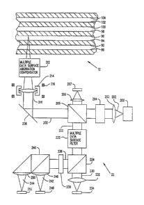
Fig. 1 shows a schematic diagram of an optical data storage system of the
present
invention and is designated by the general reference number 10. System 10
includes an optical
data storage medium 12 which is preferably disk shaped. Medium 12 is removably
mounted on a
clamping spindle 14 as is known in the art. Spindle 14 is attached to a
spindle motor 16 which in
turn is attached to a system chassis 20. Motor 16 rotates spindle 14 and
medium 12.
An optical head 22 is positioned below medium 12. Head 22 is attached to an
arm 24
which in turn is connected to an actuator device, such as a voice coil motor
26. Voice coil motor
26 is attached to chassis 20. Motor 26 moves arm 24 and head 22 in a radial
direction below
medium 12.
The Optical Medium
Fig. 2A is a cross-sectional view of medium 12. Medium 12 has a substrate 50.
Substrate 50 is also known as the face plate or cover plate and is where the
laser beam enters
medium 12. An outer diameter (OD) rim 52 and an inner diameter (ID) rim 54 are
attached
between face plate 50 and a substrate 56. An OD rim 58 and an ID rim 60 are
attached between
substrate 56 and a substrate 62.
An OD rim 64 and an ID rim 66 are attached between substrates 62 and a
substrate 68.
An OD rim 70 and ID rim 72 are attached between substrates 68 and a substrate
74. Face plate
SO and substrates 56, 62, 68 and 74 are made of a light transmissive material
such as glass,
polycarbonate or other polymer material. In a preferred embodiment, face plate
50 is 1.2 mm
thick and substrates 56, 62, 68 and 74 are 0.4 mm thick. The substrate may
alternatively have
thicknesses of 0.2 to 0.8 mm. The ID and OD rims are preferably made of a
plastic material and
SA9-91-020F 4
CA 02271541 1999-OS-19
are approximately 500 microns thick. The rims may alternatively have
thicknesses of 50-500
microns.
The rims may be attached to the face plate and substrates by means of glue,
cement or other
bonding process. The rims may alternatively be integrally formed in the
substrates. When in
place, the rims form a plurality of annular spaces 78 between the substrates
and the face plate. A
spindle aperture 80 passes through medium 12 inside the ID rims for receiving
the spindle 14. A
plurality of passages 82 are provided in the ID rims connecting the aperture
and the spaces 78 to
allow pressure equalization between the spaces 78 and the surrounding
environment of the disk
file, which would typically be air. A plurality of low impedance filters 84
are attached to
passages 82 to prevent contamination of spaces 78 by particulate matter in the
air. Filters 84 may
be quartz or glass fiber. Passages 82 and filters 84 could alternatively be
located on the OD rim.
Surfaces 90, 92, 94, 96, 98, l00, 102 and 104 are data surfaces and lie
adjacent spaces 78.
These data surfaces may contain ROM data which is formed directly into the
substrate surfaces
or, alternatively the data surfaces may be coated with one of the various
writeable optical storage
films such as WORM, or one of the various erasable optical storage films such
as phase change,
or magneto-optical. Other than the optical storage films themselves, the data
surfaces are made
without the separate metallic reflector layer structures (reflectivity from 30-
l00%) which are
known in the prior art such as US Patent 4,450,553. In other words, the data
surfaces may
comprise, consist of or essentially consist of the surface itself in the case
of a ROM surface or the
surface and an optical storage film in the case of WORM, phase change or
magneto-optic
surfaces. An additional nondata storing reflector layer is not needed. The
result is that the data
surfaces are very light transmissive and many data surfaces are possible.
Although the
intermediate data surfaces do not have reflector layers, a reflector layer may
optionally be added
behind the last data surface 104 to achieve greater reflection from the last
data surface 104.
In the preferred embodiment, the data surfaces are ROM surfaces. Data is
permanently
recorded as pits which are formed directly into the substrate at the time the
disk is manufactured.
In contrast to the prior art, the ROM surfaces of the present invention do not
have metallic
reflector layers. The substrates have no coatings. The result is that the
transmissivity of each
data surface is approximately 96%. The 4% reflectivity is sufficient to detect
the data. The high
transmissivity has the benefit of allowing a large number of data surfaces to
be accessed and
minimizes the effects of unwanted signals from other surfaces. Since there are
no coatings on
these surfaces, they are easier to manufacture and are more resistant to
corrosion.
Although it is not necessary, it may be desirable to increase the reflectivity
to reduce the
required laser power. One way to increase the reflectivity above 4% is to
apply a thin film
SA9-91-020F 5
CA 02271541 1999-OS-19
coating of a dielectric which has an index of refraction greater than the
substrate. The maximum
reflectivity of 20% occurs at a dielectric thickness of approximately
~,/4n,and varies
monotonically to a minimum reflectivity of 4% at a thickness of approximately
~,/2n, where 7~ is
the wavelength of the light and n is the index of refraction of the
dielectric. Examples of such
dielectric materials are Zr02, ZnS, SiNx or mixed oxides. The dielectric may
be deposited by
sputtering as is known in the art.
The reflectivity of the data layer can also be reduced below 4%. This
increases the
transmittance and allows more disks to be stacked. The reduction in
reflectivity occurs when a
dielectric film which has an index of refraction less than the substrate is
used. One such
I 0 dielectric is MnF which has a index of refraction of 1.35. The minimum
reflectivity of 1
occurs at a dielectric thickness of approximately 7./4n, and varies
monotonically to a maximum
reflectivity of 4% at a thickness of approximately 7J2n, where ~, is the
wavelength of the light
and n is the index of refraction. There are many other thin film anti-
reflection materials which
could also be used. These anti-reflection films may be applied by sputtering
processes as are
known in the art.
The data surfaces may alternatively contain WORM data. WORM films such as
tellurium-selenium alloys or phase change WORM films may be coated onto the
data surfaces.
The films are vacuum deposited by sputtering or evaporation onto the substrate
as is known in
the art. The amount of reflection, absorption, and transmission of each film
is related to its
thickness and optical constants. In a preferred embodiment, tellurium-selenium
alloy is
deposited at a thickness of 20-800 Angstroms.
The data surface may alternatively contain reversible phase change films. Any
type of
phase change films may be used, however, preferred compositions include those
that lie along or
close to the tieline connecting GeTe and Sb2Te3, which include
Te52.5Ge15.3Sb33'
Ge2Sb2Te5, GeSb2Te4 and GeSb4Te~. The films are vacuum deposited by sputtering
processes
as are known in the art onto the substrate to a thickness between 20-800
Angstroms. An optional
protective overcoat of 3,000 Angstroms of dielectric may be formed on top of
the phase change
film in order to help prevent ablation.
Data surfaces may also alternatively contain magneto-optical films. Magneto-
optical film
such as rare earth transition metals are vacuum deposited by sputtering
processes as are known in
the art onto the substrate to a thickness of 20-800 Angstroms.
A further alternative is to have the data surfaces contain a combination of
ROM, WORM,
or erasable media. The higher transmission surfaces such as ROM are preferably
located closer
to the light source and the lower transmission surfaces such as WORM, phase
change and
SA9-91-020F 6
CA 02271541 1999-OS-19
magneto-optical are preferably located furthest away. The dielectric and anti-
reflection films
described above with the ROM surface may also be used with WORM and erasable
media.
Fig. 2B is a cross-sectional view of an alternative embodiment of an optical
recording
medium and is designated by the general reference number 120. Elements of
medium 120 which
are similar to elements of medium 12 are designated by a prime number. Medium
l20 does not
have the rims and spaces 78 of medium 12. Instead, a plurality of solid
transparent members l22
separates the substrates. Members 122 are made of a material having a
different index of
refraction than the substrates. This is necessary to achieve some reflection
at the data surfaces.
In a preferred embodiment, the members 122 are made of an optical cement which
also serves to
hold the substrate together. The thickness of members 122 is preferably
approximately 100-300
microns. Medium l20 may be substituted for medium 12 in system 10.
Fig. 3A shows an exaggerated detailed cross-sectional view of a preferred data
surface
pattern of medium 12 and is designated by the general reference number 130.
Surface 90
contains a pattern of spiral (or alternatively concentric) tracking grooves
l32. The portions of
surface 90 located between the grooves 132 are known as the land portions 134.
Surface 92
contains a pattern of spiral inverse tracking grooves (raised ridges) 136. The
portion of surface
92 located between the inverse grooves 136 is the land l38. The grooves 132
and the inverse
grooves 136 are also referred to as tracking marks. In a preferred embodiment,
the widths 140 of
the tracking marks are 0.6 microns and the width 142 of the land sections is
1.0 microns. This
results in a pitch of (1.0 + 0.6) = 1.6 microns.
The tracking marks are used to keep the light beam on track while the medium
12 rotates.
This is described in more detail below. For pattern l30, a beam 144 from the
optical head 22
will track on the land portion 134 or l38 depending upon which surface it is
focussed upon. The
recorded data is on the land portions. In order for the tracking errors signal
(TES) to be of equal
magnitude for both surfaces 90 and 92 the optical path difference between
light reflected from
the lands and tracking marks must be the same for both surfaces. Beam 144
focuses on surface
90 through substrate 50, however, beam 144 focuses on surface 92 through space
78. In the
preferred embodiment space 78 contains air. For the optical path length
difference between the
lands and tracking marks to be the same d 1 n 1 must equal d2n2 (or d2/d 1
equals n 1 /n2), where d 1
is the depth of mark 132 (perpendicular distance), nl is the index of
refraction of substrate 50, d2
is the height of mark 136 (perpendicular distance), and n2 is the index of
refraction of space 78.
In a preferred embodiment, space 78 contains air which has an index of
refraction of 1.0 and
substrate 50 (as well as the other substrates) has an index of refraction 1.5.
So the ratio of d2/dl
equals 1.5. In a preferred embodiment, dl is 700 Angstroms and d2 is 1050
Angstroms. The
SA9-91-020F 7
CA 02271541 1999-OS-19
same pattern of tracking marks is repeated on the other surfaces of medium 12.
The other
substrate incident surfaces 94, 98 and l02 are similar to surface 90 and the
other space incident
surfaces 96, 100 and 104 are similar to surface 92.
Although the tracking marks are preferably arranged in a spiral pattern, they
may
alternatively be in a concentric pattern. In addition, the spiral pattern may
be the same for each
data surface, i.e., they are all clockwise or counter-clockwise spirals, or
they may alternate
between clockwise and counter-clockwise spiral patterns on consecutive data
layers. This
alternating spiral pattern may be preferable for certain applications, such as
storage of video data,
movies for example, where continuous tracking of data is desired. In such a
case, the beam
tracks the clockwise spiral pattern inward on the first data surface until the
spiral pattern ends
near the inner diameter, and then the beam is refocused on the second data
surface directly below
and then the beam tracks the counter-clockwise spiral pattern outward until
the outer diameter is
reached.
Fig. 3B shows an exaggerated detailed cross-sectional view of an alternative
surface
pattern for medium 12 and is designated by the general reference number 150.
Pattern 150 is
similar to pattern 130 except that the tracking marks for surface 92 are
grooves 152 instead of
inverse grooves. The pitch and the ratio of d2/dl are the same as for pattern
l30. Beam 144 will
track on land 134 on surface 90, but now beam 144 will track on groove 152
when focussed on
surface 92. Tracking in the groove 132 may be desirable in certain situations.
However, as will
be described below, beam 144 may also be electronically controlled to track on
land 138 of
surface 92. The tracking marks for surfaces 94, 98 and 102 are similar to
surface 90 and the
surfaces 96, l00 and 104 are similar to surface 92.
Fig. 3C shows an exaggerated detailed cross-sectional view of an alternative
surface
pattern for medium 12 which is designated by the general reference number 160.
Pattern 160 is
similar to pattern l30 except that surface 90 has inverse grooves 162 instead
of grooves 132, and
surface 92 has grooves 164 instead of inverse grooves l36. The pitch and ratio
of d2/dl are the
same as for pattern 130. Beam 144 will track on inverse grooves 162 when
focussed on surface
90 and will track on grooves 164 when focussed on surface 92(unless it is
electronically switched
to track on the land). The pattern for surfaces 94, 98 and 102 are similar to
surface 90 and the
surfaces 96, 100 and 104 are similar to surface 92.
Fig. 3D shows an exaggerated detailed cross-sectional view of an alternative
surface
pattern designated by the general reference number 170. In pattern 170, the
surface 90 has a
similar structure to surface 90 of pattern 160. Surface 92 has a similar
structure to surface 92 of
pattern 130. The pitch and ratio of d2/dl is the same as for pattern 130. Beam
144 will track on
SA9-91-020F 8
CA 02271541 1999-OS-19
inverse grooves 162 when focussed on surface 90 (unless it is electronically
switched to track on
the land) and will track on land 138 when focussed on surface 92. Surfaces 94,
98 and 102 have
similar patterns to surface 90 and surfaces 96, l00 and 104 have patterns
similar to surface 92.
For all of the patterns l30, 150, 160 and 170 the tracking marks are formed
into the
substrate at the time of manufacture by injection molding or photopolymer
processes as are
known in the art. It should be noted that the optical films, as described
above, are deposited onto
the substrates after the tracking marks are formed.
The discussion of tracking marks is also applicable to other features of
optical disks. For
example, some ROM disks use pits embossed in the substrate to record data
and/or provide
tracking information. Other optical media use pits to emboss sector header
information. Some
media use these header pits to also provide tracking information. In using
such media in the
multiple data surface form of the present invention, the pits are formed as
pits or inverse pits on
the various data surfaces corresponding in a similar manner to the tracking
marks discussed
above. The optical path length between the lands and the pits or inverse pits
is also similar to the
tracking marks. The pits, inverse pits, grooves and inverse grooves are all
located at a different
elevation from the land ( i.e. the perpendicular distance between them and the
land), and are all
referred to as marks for purposes of this discussion. Marks which are
specifically dedicated to
providing tracking information are known as nondata tracking marks.
The Optical Head
Fig. 4 shows a schematic diagram of an optical head 22 and medium 12. Optical
head 22
has a laser diode 200. Laser 200 may be a gallium-aluminum-arsenide diode
laser which
produces a primary beam of light 202 at approximately 780 nanometers
wavelength. Beam 202
is collimated by lens 203 and is circularized by a circularizer 204 which may
be a circularizing
prism. Beam 202 passes to a beamsplitter 205. A portion of beam 202 is
reflected by
beamsplitter 205 to a focus lens 206 and an optical detector 207. Detector 207
is used to monitor
the power of beam 202. The rest of beam 202 passes to and is reflected by a
mirror 208. Beam
202 then passes through a focus lens 210 and a multiple data surface
aberration compensator 2l2
and is focused onto one of the data surfaces (surface 96 as shown) of medium
12. Lens 210 is
mounted in a holder 214. The position of holder 214 is adjusted relative to
medium 12 by a
focus actuator motor 216 which may be a voice coil motor.
A portion of the light beam 202 is reflected at the data surface as a
reflected beam 220.
Beam 220 returns through compensator 212 and lens 210 and is reflected by
mirror 208. At
beamsplitter 205, beam 220 is reflected to a multiple data surface filter 222.
The beam 220
SA9-91-020F 9
CA 02271541 1999-OS-19
passes through filter 222 and passes to a beamsplitter 224. At beamsplitter
224 a first portion
230 of beam 220 is directed to an astigmatic lens 232 and a quad optical
detector 234. At
beamsplitter 224 a second portion 236 of beam 220 is directed through a half
wave plate 238 to a
polarizing beamsplitter 240. Beamsplitter 240 separates light beam 236 into a
first orthogonal
S polarized light component 242 and a second orthogonal polarized light
component 244. A lens
246 focuses light 242 to an optical detector 248 and a lens 2S0 focuses light
244 to an optical
detector 2S2.
Fig. S shows a top view of a quad detector 234. The detector 234 is divided
into four
equal sections 234A, B, C and D.
Fig. 6 shows a circuit diagram of a channel circuit 260. Circuit 260 comprises
a data
circuit 262, a focus error circuit 264 and a tracking error circuit 266. Data
circuit 262 has an
amplifier 270 connected to detector 248 and an amplifier 272 connected to
detector 2S2.
Amplifiers 270 and 272 are connected to a double pole, double throw electronic
switch 274.
Switch 274 is connected to a summing amplifier 276 and a differential
amplifier 278.
1 S Circuit 264 has a plurality of amplifiers 280, 282, 284 and 286 connected
to detector
sections 234A, B, C and D, respectively. A summing amplifier 288 is connected
to amplifiers
280 and 284, and a summing amplifier 290 is connected to amplifiers 282 and
286. A
differential amplifier 292 is connected to summing amplifiers 288 and 290.
Circuit 266 has a pair of summing amplifiers 294 and 296, and a differential
amplifier
298. Summing amplifier 294 is connected to amplifiers 280 and 282, and summing
amplifier
296 is connected to amplifiers 284 and 286. Differential amplifier 298 is
connected to summing
amplifiers 294 and 296 via a double pole double throw electronic switch 297.
Switch 297 acts to
invert the inputs to amplifier 298.
Fig. 7 is a schematic diagram of a controller system of the present invention
and is
2S designated by the general reference number 300. A focus error signal (FES)
peak detector 310 is
connected to the focus error signal circuit 264. A track error signal (TES)
peak detector 312 is
connected to the tracking error signal circuit 266. A controller 314 is
connected to detector 310,
detector 312, detector 207 and circuits 262, 264 and 266. Controller 314 is a
microprocessor
based disk drive controller. Controller 314 is also connected to and controls
the laser 200, head
motor 26, spindle motor 16, focus motor 216, switches 274 and 297, and
compensator 212. The
exact configuration and operation of compensator 212 is described in more
detail below.
The operation of system 10 may now be understood. Controller 314 causes motor
16 to
rotate disk 12 and causes motor 26 to move head 22 to the proper position
below disk 12. See
Fig. 4. Laser 200 is energized to read data from disk 12. The beam 202 is
focussed by lens 210
SA9-91-020F 10
CA 02271541 1999-OS-19
on the data surface 96. The reflected beam 220 returns and is divided into
beams 230, 242 and
244. Beam 230 is detected by detector 234 and is used to provide focus and
tracking servo
information, and beams 242 and 244 are detected by detectors 248 and 252,
respectively, and are
used to provide data signals.
See Fig. 5. When beam 202 is exactly focussed on data surface 96, beam 230
will have a
circular cross-section 350 on detector 234. This will cause circuit 264 to
output a zero focus
error signal. If beam 202 is slightly out of focus one way or the other, beam
230 will fall as an
oval pattern 352 or 354 on detector 234. This will cause circuit 264 to output
a positive or
negative focus error signal. Controller 314 will use the focus error signal to
control motor 216 to
move lens 2l0 until the zero focus error signal is achieved.
If beam 202 is focussed exactly on a track of data surface 96, then beam 230
will fall as a
circular cross-section 350 equally between the sections A and B, and the
sections D and C. If the
beam is off track it will fall on the boundary between a tracking mark and the
land. The result is
that the beam is diffracted and cross-section 350 will move up or down. More
light will be
received by sections A and B, and less by sections C and D or vice versa.
Fig. 8A shows a graph of the TES produced by circuit 264 versus the
displacement of
head 22. Controller 314 causes VCM 26 to move head 22 across the surface of
medium 12. TES
peak detector 312 counts the peaks (maximum and minimum points) of the TES
signals. There
are two peaks between each track. By counting the number of peaks, controller
314 is able to
position the beam on the proper track. The TES signal at a land is a positive
slope TES signal.
Controller 314 uses this positive slope signal to lock the beam on track. For
example, a positive
TES signal causes head 22 to move to the left toward the zero point land
position and a negative
TES signal causes the head 22 to move to the right toward the zero point land
position. Fig. 8A
is the signal derived from the preferred pattern 130 of medium 12 when switch
297 is in its initial
position as shown in Fig. 6. The same signal is also generated for surface 90
of pattern l50, and
surface 92 of pattern l70. The beam is automatically locked to the land
because that is the
position where there is a positive slope.
Fig. 8B shows a graph of the TES versus head displacement for surface 92 of
pattern
150, surfaces 90 and 92 of pattern 160 and surface 90 of pattern 170 when
switch 297 is in its
initial position. Note that in this case the tracking marks are such that the
positive slope signal
occurs at the location of the tracking marks and so that the beam will
automatically track on the
tracking marks and not the land portions. Tracking on the tracking marks may
be desirable in
some circumstances.
Fig. 8C shows a graph of the TES versus head displacement for surface 92 of
pattern
SA9-91-020F 11
CA 02271541 1999-OS-19
150, surfaces 90 and 92 of pattern 160 and surface 90 of pattern 170 when
inverter switch 297 is
enabled such that the TES signal is inverted. The TES now has a positive slope
at the land
positions and the beam will track on the land portion instead of the tracking
marks. Thus,
controller 314 can track the grooves or the lands by setting switch 297.
In the preferred embodiment, medium 12 contains ROM data surfaces.
Reflectivity
detection is used to read the ROM data. In data circuit 262, switch 274 is
positioned to connect
amplifier 276 when a ROM disk is to be read. The signal from detectors 248 and
252 is added.
Less light is detected where data spots have been recorded and this difference
in light detected is
the data signal. Switch 274 will have the same setting for reading WORM and
phase change data
disk. If disk 12 has magneto-optical data surfaces, then polarization
detection is needed to read
the data. Switch 274 will be set to connect amplifier 278. The difference in
the orthogonal
polarization light detected at detectors 248 and 252 will then provide the
data signal.
Fig. 9 shows a graph of the focus error signal from circuit 264 versus the
displacement
distance of lens 2l0. Note that a nominally sinusoidal focus error signal is
obtained for each of
the data surfaces of medium 12. Between the data layers, the focus error
signal is zero. During
startup of the system, controller 3l4 first causes motor 216 to position lens
2l0 at its zero
displacement position. Controller 3l4 will then seek the desired data surface
by causing motor
2l6 to move lens 210 in a positive displacement direction. At each data layer,
peak detector 310
will detect the two peaks of the focus error signal. Controller 314 will count
the peaks (two per
data surface) and determine the exact data surface on which beam 202 is
focussed. When the
desired surfaces are reached, controller 314 causes motor 216 to position lens
210 such that the
focus error signal is between the two peaks for that particular data surface.
The focus error is
then used to control the motor 2l6 to seek the zero point focus error signal
between the peaks,
i.e. lock on the positive slope signal such that exact focus is achieved. The
controller 3l4 will
also adjust the power of laser 200, the switch 297, and the aberration
compensator 2l2 as
appropriate for that particular data surface.
Also on startup, controller 314 determines what type of disk it is reading.
Switch 274 is
first positioned for reflectivity detection and switch 297 is set to read the
land portions of the disk
of the preferred pattern l30. The controller 314 seeks and reads the header
information of the
first track of the first data surface. The header has information on the
number of layers, what
type of optical media is in each layer (reflectivity or polarization
detection), and what type of
tracking mark patterns are used. With this information, the controller 314 is
able to set switches
274 and 297 to correctly read each data surface. For example, the disk may
have four layers of
ROM data surfaces and two layers of MO data surfaces. Controller 314 will set
switch 274 to
SA9-91-020F 12
CA 02271541 1999-OS-19
reflectivity detection for surfaces 1-4 and to polarization detection for
surfaces 5-6.
If controller 314 is unable to read the first track of the first data surface
(perhaps the first
layer has a different tracking mark pattern), then controller 314 will set
switch 297 to its other
setting and will attempt to read the first track of the first data surface
again. If this still does not
work (perhaps the first data surface is magneto-optic and requires
polarization detection) then the
controller will set switch 274 to the polarization detection and try again,
setting switch 297 at one
setting and then the other. In summary, controller 314 will read the header
information of the
first track of the first data surface by trying the four different
combinations of settings of
switches 274 and 297 until it is successful at reading the track. Once
controller 314 has this
header information, it can correctly set the switches 274 and 297 for each of
the other data
surfaces.
Alternatively, the disk drive may be specifically dedicated to work with only
one type of
medium. In that case, controller 314 is preprogrammed to store information on
the type of data
surfaces, number of layers, and types of tracking marks.
The Aberration Compensator
Lenses are typically designed to focus light through air which has an index of
refraction
of 1Ø When such lenses focus light through materials having different
indices of refraction, the
light experiences a spherical aberration, which distorts and enlarges the beam
spot, degrading the
reading and recording performance.
In typical optical data storage systems, there is only one data surface onto
which to focus.
The data surface is usually located beneath a 1.2 mm thick face plate. The
lens is typically a .55
numerical aperture (NA) lens which is specially designed to correct for
spherical aberration
caused on the light by the 1.2 mm face plate. The result is that a good spot
focus can be obtained
at that exact depth, but at other depths the focus gets blurry. This causes
severe problems for any
multiple data layer system.
The aberration compensator 2l2 of the present invention solves this problem.
Fig. 10
shows a schematic diagram of an aberration compensator which is designated by
the general
reference number 400 and may be used as compensator 2l2. Compensator 400
comprises a
stepped block 402 having three steps. A first step 404 has a thickness of 0.4
mm, a second step
406 has a thickness of 0.8 mm and a third step 408 has a thickness of 1.2 mm.
The block 402 is
made of the same material as the face plate and substrates of medium 12 or
other similar optical
material. Note that these steps increase in optical thickness in increments of
the substrate
thickness. Block 402 is attached to a voice coil motor 4l0 (or similar
actuator device) which in
SA9-91-020F 13
CA 02271541 1999-OS-19
turn is connected to controller 3l4. Motor 410 moves block 402 laterally into
and out of the path
of beam 302.
Lens 210 is designed to focus on the lowest data surface of medium 12. In
other words,
lens 210 is designed to compensate for spherical aberrations caused by the
combined thicknesses
of the face plate and the intervening substrates. For the present invention,
in order to focus on
surface 102 or 104, beam 202 must pass through the face plate 50 and
substrates 56, 62 and 68 (a
combined thickness of 2.4 mm of the substrate material). Note that the air
spaces 78 are not
counted because they impart no additional spherical aberration. Lens 210 is
thus designed to
focus through 2.4 mm of polycarbonate and may focus equally well on both data
surfaces 102
and 104.
When beam 202 is focussed on either surface 102 or 104, the block 402 is
completely
withdrawn and beam 202 does not pass through it. When beam 202 is focussed on
surface 98 or
100, block 402 is positioned such that beam 202 passes through step 404. When
beam 202 is
focussed on surfaces 94 or 96, block 402 is positioned such that beam 202
passes through step
406. When beam 202 is focussed on surfaces 90 or 92, block 402 is positioned
such that beam
202 passes through step 408. The result is that no matter which pair of
surfaces are focussed on,
beam 202 will always pass through the same total optical thickness of material
and will not
experience spherical aberration problems. Controller 314 controls motor 410 to
move the block
402 as appropriate.
Fig. 11 shows an aberration compensator which is designated by the general
reference
number 430 and which may be used for compensator 212. Compensator 430 has a
pair of
complementary triangular shaped blocks 432 and 434. Blocks 432 and 434 are
made of the same
material as face plate and substrates of medium 12 or material of similar
optical properties.
Block 432 is positioned in a fixed position such that beam 202 passes through
it. Block 434 is
attached to a voice coil motor 436 and may be slid along the surface of block
432. Controller
314 is connected to and controls motor 436. By moving block 434 relative to
block 432 the
overall thickness of material through which beam 202 passes may be adjusted.
The result is that
beam 202 passes through the same optical thickness of material no matter which
data surface it is
focussed on.
Figs. 12 and 13 show an aberration compensator which is designated by the
general
reference number 450 and may be used for compensator 2l2. Compensator 4S0 has
a circular
stepped element 452. Element 452 has four sections 454, 456, 458 and 460.
Sections 456, 458
and 460 have thicknesses similar to steps 404, 406 and 408, respectively, of
compensator 400.
Section 454 has no material and represents a blank space in the circular
pattern as shown in Fig.
SA9-91-020F 14
CA 02271541 1999-OS-19
13. The circular element 452 is attached to a stepper motor 462 which in turn
is controlled by
controller 314. Spindle 462 rotates element 452 such that beam 202 passes
through the same
thickness of material no matter which data surface it is focussed on.
Fig. 14 shows an aberration compensator which is designated by the general
reference
number 570 and may be used for compensator 2l2. Compensator 570 comprises a
stationary
convex lens 572 and a moveable concave lens 574. Lens 574 is attached to a
voice coil motor
576. Voice coil motor 576 is controlled by controller 3l4 to move lens 574
relative to lens 572.
Beam 202 passes through lens 572, lens 574 and lens 210 to medium 12. Moving
lens 574
relative to lens 572 changes the spherical aberration of beam 202 and allows
it to focus on the
different data surfaces. In a preferred embodiment lenses 210, S74 and 572
comprise a Cooke
triplet having movable center element 574. Cooke triplets are described in
more detail in the
article by R. Kingslake, "Lens Design Fundamentals," Academic Press, New York,
1978, pp.
286-295. Although lens 274 is shown as the moving element, alternatively, lens
574 could be
stationary and lens 572 used as the moving element. In Fig. 4 the aberration
compensator 212 is
shown between lens 210 and medium 12. However, if compensator 570 is used it
will be located
between lens 210 and mirror 208 as shown in Fig. 14.
Fig. 15 shows an aberration compensator which is designated by the general
reference
number 580. Compensator 580 comprises an aspheric lens element 582 with
nominally zero
focal power. Element 582 has a spherical aberration surface 584 and a planar
surface 586. Lens
582 is connected to a voice coil motor 588. Voice coil motor 588 is controlled
by controller 314
which moves lens 582 relative to lens 512. Beam 202 passes through lens 210
and lens 582 to
medium 12. Moving lens 582 relative to lens 210 changes the spherical
aberration of the beam
202 and allows it to focus on the different data surfaces.
Fig. 16 shows a view of lens 582 relative to axes z and p. In a preferred
embodiment, the
surface of 584 should correspond to the formula Z=0.00770p4-0.00154p6.
Fig. 17 shows a schematic diagram of an alternative optical head of the
present invention
and is designated by the general reference number 600. Elements of head 600
which are similar
to elements of head 22 are designate by a prime number. Note that head 600 is
similar to system
10 except that the aberration compensator 212 has been eliminated and a new
aberration
compensator 602 has been added between beamsplitter 206' and mirror 208'. The
description and
operation of compensator 602 is described below. The operation of head 600 is
otherwise the
same as described for head 22. Head 600 may be substituted for head 22 in
system 10.
Fig. 18 shows a schematic diagram of an aberration compensator which is
designated by
the general reference number 610 and may be used for compensator 602.
Compensator 610
SA9-91-020F 15
CA 02271541 1999-OS-19
comprises a substrate 6l2 having a reflective holographic coating 614.
Substrate 612 is attached
to a stepper motor 616 which in turn is controlled by controller 314.
Holographic coating 614
has a number of different holograms recorded, each of which imparts a
particular spherical
aberration to beam 202'. These holograms are of the Bragg type which are
sensitive only to light
S incident at a specific angle and wavelength. When substrate 612 is rotated a
few degrees, beam
202' will experience a different hologram. The number of holograms recorded
corresponds to the
number of different spherical aberration corrections required. For medium 12
as shown, four
different recordings are necessary each corresponding to one of the pairs of
data surfaces.
Fig. 19 shows a schematic diagram of an aberration compensator which is
designated by
the general reference number 620 and may be used for compensator 602.
Compensator 620
comprises a substrate 622, a transmissive holographic coating 624 and a
stepper motor 626. The
compensator 620 is similar to compensator 610 except that here the holographic
coating 624 is
transmissive rather than reflective. Holographic coating 624 has a number of
holograms
recorded, each of which corresponds to the amount of spherical aberration
compensation
1 S required. Beam 202' experiences each of these holograms in turn as
substrate 622 is rotated.
Fig. 20 shows a schematic diagram of a recording system used to make the
holographic
coatings 614 and 624, and is designated by the general reference number 6S0.
System 6S0 has a
laser 6S2 which produces a light beam 6S4 at a frequency similar to the laser
200. Light 6S4 is
collimated by lens 6S6 and is passed to a beamsplitter 6S 8. Beamsplitter 6S 8
divides the light
into a beam 66Q and a beam 662. Beam 660 is reflected by a mirror 664 and 666,
and is focussed
by a lens 668 to a point 670 in a plane 672. Beam 660 passes through a stepped
block 674
similar to block 402. Beam 660 is then recollimated by a lens 676 and falls
upon a holographic
coating 680 on a substrate 682. Substrate 682 is rotatably mounted to a
stepper motor 684. Beam
662 also falls upon coating 680 at a 90 degree angle from beam 660.
2S Lens 668 forms an unaberrated spot on plane 672. This light is then passed
through a
step of block 674 which has a thickness representing the sum of the substrate
thicknesses which
will be encountered in accessing a particular recording layer. Lens 676 is
identical in design to
lens 210 as used in the optical storage head. It collimates the light into a
beam that contains a
specific amount of spherical aberration corresponding to the specific
thickness. This wavefront
is holographically recorded by interference with the reference beam 662. If
the hologram is
oriented in approximately a plane 690 as shown, a transmission hologram is
recorded. If it is
oriented in approximately a plane 692 as shown as a dash line, a reflective
hologram is recorded.
The wavefront required to correct the aberrations encountered in accessing a
different pair of
recording layers is holographically stored by rotating the hologram to a new
angular position and
SA9-91-020F 16
CA 02271541 1999-OS-19
inserting the corresponding thickness plate of block 674. A multiplicity of
angularly resolved
holograms are recorded, each corresponding to and providing correction for a
different pair of
recording layers. The holographic coating may be made of dichromated gelatin
or a
photopolymer material. The individual holograms can be recorded in increments
as small as one
degree without appreciable cross-talk. This permits large numbers of holograms
to be recorded
and correspondingly large numbers of data surfaces to be used.
Fig. 21 shows a schematic diagram of an alternative aberration compensator
which is
designated by the general reference number 700 and may be used for compensator
602.
Compensator 700 comprises a polarizing beamsplitter 702, a quarter waveplate
704, a carousel
706 attached to a stepper motor 708 and a plurality of spherical aberration
mirrors 710 each
providing a different spherical aberration correction. Beam 202' is oriented
with its polarization
such that it passes through beamsplitter 702 and plate 704 to one of mirrors
7l0. Mirror 710
imparts the appropriate spherical aberration to the beam 202' which then
returns through plate
704 and is reflected by beamsplitter 702 to mirror 208'. Motor 708 is
controlled by controller
314 to rotate the carousel 706 to position the appropriate mirror in place.
Mirrors 7l0 are
reflecting Schmidt corrector plates. See M. Born, et al., "Principles of
Optics," Pergonan Press
Oxford, 1975, pp. 245-249.
Fig. 22 shows a schematic diagram of an aberration compensator which is
designated by
the general reference number 720 and may be used for compensator 602.
Compensator 720
comprises a polarizing beamsplitter 722, a quarter waveplate 724 and an
electrical controlled
deformable mirror 726. Deformable mirror 726 is controlled by internal piezo-
electric elements
and is described in more detail in J.P. Gaffarel, et al., "Applied Optics,"
Vol. 26, pp. 3772-3777,
( 1987). The operation of compensator 720 is similar to compensator 700,
except that mirror 726
is electrically adjusted to provide the appropriate spherical aberration. In
other words, mirror
726 is adjusted to form a reflective surface corresponding to the different
Schmidt corrector
plates 7l0 of compensator 700. Controller 314 controls the adjustment of
mirror 726 as
appropriate.
The operation of the aberration compensators 212 and 602 have been described
above in
connection with medium 12. Due to the air space between the layers, one
aberration
compensation setting will work for each pair of data surfaces. However, in the
case where
medium l20 is used, aberration compensation settings will need to be made for
each data
surface. This is because there are no air spaces.
SA9-91-020F 17
CA 02271541 1999-OS-19
Multiple Data Surface Filter
When beam 202 is focussed on a particular data surface of medium 12 a
reflected beam
230 is returned to head 22 from that surface. However, some of light beam 202
is also reflected
at the other data surfaces. This unwanted reflected light must be screened out
for proper data and
servo signals to be obtained. The multiple data surface filter 222 of the
present invention
achieves this function.
Fig. 23 shows a schematic diagram of a filter 750 which may be used as filter
222. Filter
750 comprises a blocking plate 754 and a lens 756. The desired light beam 230
is collimated
because it is the light which has been properly focussed by lens 2l0. Beam 230
is focussed by
lens 752 to a point 760. Unwanted light 762 is not properly focussed by lens
210 and is thus not
collimated. The light 762 will not focus to point 760. Plate 764 has an
aperture 764 at point 760
which allows light 230 to pass. Most of the unwanted light 762 is blocked by
plate 754. The
light 230 is recollimated by lens 756. In a preferred embodiment aperture 764
is circularly
shaped and has a diameter of approximately ~,/(2*(NA)), where 7~ is the
wavelength of the light
and N.A. is the numerical aperture of lens 752. The exact diameter is
determined by the desired
trade-off between alignment tolerances and interlayer signal rejection
requirements.
Alternatively, aperture 764 may be a slit having a minimum gap distance of
approximately
7.,/(2*(NA)). In such a case plate 764 could be two separate members which are
separated by the
slit. Plate 754 may be made of a metal sheet or may be made of a transparent
substrate having a
light blocking coating with aperture 764 being uncoated.
Fig. 24 shows a schematic diagram of a filter 800 which also may be used as
filter 222.
Filter 800 comprises a lens 802, a blocking plate 804, a blocking plate 806
and a lens 808. Plate
806 has an aperture 810 located at a focal point 812 of lens 802. Plate 804
has a complementary
aperture 8l4 which allows the collimated light 230 to be directed through
aperture 810 while
blocking unwanted uncollimated light 820. Aperture 814 may be a pair of
parallel slits or an
annular aperture. In a preferred embodiment, the distance between the slits of
aperture 8l4 is
greater than the diameter of aperture 8l0. The diameter of aperture 810 is
approximately equal
to a,/(2 * (NA)). For the alternative annular shaped aperture, the inner
diameter of the annular slit
should be greater than the diameter of aperture 810. In both cases, the outer
edge 822 of aperture
814 is located outside of beam 230. Blocking plates 804 and 806 may be made of
a metal sheet
or may be made of a transparent substrate having a light blocking coating with
apertures 810 and
814 being uncoated.
Fig. 25 shows a schematic diagram of an alternative filter 830 which may be
used as
filter 222. Filter 830 comprises a beamsplitter 832 and a holographic plate
834. The coating on
SA9-91-020F 18
CA 02271541 1999-OS-19
the holographic plate 834 is tuned to efficiently reflect collimated beam 230
while uncollimated
beam 840 is allowed to pass. The desired beam 230 is reflected from
holographic plate 834 and
returns to beamsplitter 832 where it is reflected towards beamsplitter 224.
Fig. 26 is a schematic diagram which shows how holographic plate 834 is made.
A
collimated laser beam 850 having approximately the same wavelength as laser
200 is split into
two beams 852 and 854 at an amplitude beamsplitter 856. Beams 852 and 854 are
directed by
mirrors 860 and 862, respectively, and fall upon hologram plate 834 from
opposite directions
perpendicular to the surface of plate 834. A reflective hologram is recorded
by the interference
of beams 852 and 854. The holographic coating may be made of a dichromated gel
or
photopolymer material.
Filters 222 of the present invention have been shown in Fig. 4 to be located
in the path of
beam 220. However, one or more filters can be located in the separate paths of
servo beam 230
or the data beam 236.
While the preferred embodiments of the present invention have been illustrated
in detail,
it should be apparent that modifications and adaptations to those embodiments
may occur to one
skilled in the art without departing from the scope of the present invention
as set forth in the
following claims.
SA9-91-020F 19